
Subscribe to Our Youtube Channel
Related Manuals for Aaeon COM-ICDB7


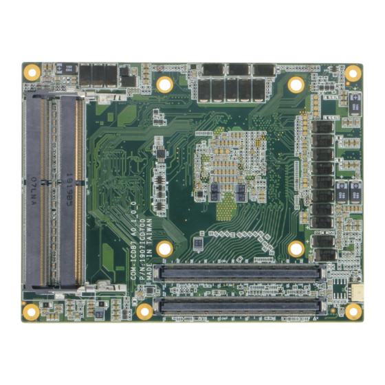
Summary of Contents for Aaeon COM-ICDB7
- Page 1 COM-ICDB7 COM Express CPU Module User’s Manual 1 Last Updated: August 11, 2022...
- Page 2 AAEON assumes no liabilities resulting from errors or omissions in this document, or from the use of the information contained herein. AAEON reserves the right to make changes in the product design without notice to its users.
- Page 3 Acknowledgements All other products’ name or trademarks are properties of their respective owners. Microsoft Windows is a registered trademark of Microsoft Corp. ⚫ Intel® and Celeron® are registered trademarks of Intel Corporation ⚫ Intel Core™ is a trademark of Intel Corporation ⚫...
- Page 4 Packing List Before setting up your product, please make sure the following items have been shipped: Item Quantity COM-ICDB7 ⚫ If any of these items are missing or damaged, please contact your distributor or sales representative immediately. Preface...
- Page 5 (if any), its specifications, dimensions, jumper/connector settings/definitions, and driver installation instructions (if any), to facilitate users in setting up their product. Users may refer to the product page at AAEON.com for the latest version of this document. Preface...
- Page 6 Safety Precautions Please read the following safety instructions carefully. It is advised that you keep this manual for future references All cautions and warnings on the device should be noted. Make sure the power source matches the power rating of the device. Position the power cord so that people cannot step on it.
- Page 7 If any of the following situations arises, please the contact our service personnel: Damaged power cord or plug Liquid intrusion to the device iii. Exposure to moisture Device is not working as expected or in a manner as described in this manual The device is dropped or damaged Any obvious signs of damage displayed on the device...
- Page 8 FCC Statement This device complies with Part 15 FCC Rules. Operation is subject to the following two conditions: (1) this device may not cause harmful interference, and (2) this device must accept any interference received including interference that may cause undesired operation.
- Page 9 China RoHS Requirements (CN) 产品中有毒有害物质或元素名称及含量 AAEON Main Board/ Daughter Board/ Backplane 有毒有害物质或元素 部件名称 铅 汞 镉 六价铬 多溴联苯 多溴二苯醚 (Pb) (Hg) (Cd) (Cr(VI)) (PBB) (PBDE) 印刷电路板 ○ ○ ○ ○ ○ ○ 及其电子组件 外部信号 ○ ○ ○ ○ ○ ○...
- Page 10 China RoHS Requirement (EN) Poisonous or Hazardous Substances or Elements in Products AAEON Main Board/ Daughter Board/ Backplane Poisonous or Hazardous Substances or Elements Hexavalent Polybrominated Polybrominated Component Lead Mercury Cadmium Chromium Biphenyls Diphenyl Ethers (Pb) (Hg) (Cd) (Cr(VI)) (PBB) (PBDE) PCB &...
-
Page 11: Table Of Contents
Table of Contents Chapter 1 - Product Specifications..................1 Specifications ......................2 Chapter 2 – Hardware Information ..................4 Dimensions ....................... 5 Switches and Connectors ..................8 List of Connectors ....................10 2.3.1 AT/ATX Switch (SW1) .................. 10 2.3.2 Battery (CN3) ....................10 2.3.3 EC Programming Header (CN4) .............. - Page 12 SIO Configuration ..................39 3.4.5 Serial Port Configuration ................40 3.4.6 Serial Port Console Redirection ...............41 3.4.7 AAEON BIOS Robot .................. 42 3.4.8 Power Management .................. 44 3.4.9 Digital IO Port Configuration ..............45 Setup Submenu: Platform Configuration ............46 3.5.1...
- Page 13 Appendix A - I/O Information ....................66 I/O Address Map ....................67 Memory Address Map ..................69 IRQ Mapping Chart ....................70 Preface XIII...
-
Page 14: Chapter 1 - Product Specifications
Chapter 1 Chapter 1 - Product Specifications... -
Page 15: Specifications
Specifications System Form Factor COM Express Basic size, Type 7 Intel®3rd Gen XEON D-1700 series CPU Frequency Up to 2.00 GHz, D-1746TER Chipset Memory Type DDR4 SODIMM Socket x 4, up to 128GB, ECC supported Max. Memory Capacity Up to 128 GB (ECC Support by SKU) If 1 &... - Page 16 Display VGA/LCD Controller Video Output Ethernet Intel® i210IT 1 GbE x 1 10GbE: 10G Base-KR to carrier x 4 Audio USB Port USB 2.0 x 4 USB 3.2 Gen 1 x 4 Serial Port 2-Wire UART(TX/RX) x 2 HDD Interface SATA III x 2 Expansion PCIe 4.0 [x16] x 1, PCIe 3.0 [x4] x 4...
-
Page 17: Chapter 2 - Hardware Information
Chapter 2 Chapter 2 – Hardware Information... -
Page 18: Dimensions
Dimensions Chapter 2 – Hardware Information... - Page 19 With DDR: Chapter 2 – Hardware Information...
- Page 20 With Heatspreader and Active Cooler: With Active Cooler: Chapter 2 – Hardware Information...
-
Page 21: Switches And Connectors
Switches and Connectors Top Side Bottom Side Chapter 2 – Hardware Information... - Page 22 Top Side with DDR Bottom Side with DDR Chapter 2 – Hardware Information...
-
Page 23: List Of Connectors
List of Connectors Please refer to the table below for all of the board’s switches and connectors that you can configure for your application Label Function AT/ATX Switch Battery EC Programming Header BIOS Programming Header ROW A/B ROW C/D CN10 CN11 LAN GPIO (i210IT) 2.3.1... -
Page 24: Ec Programming Header (Cn4)
2.3.3 EC Programming Header (CN4) Signal SPI_MISO SPI_CLK +3.3VSB SPI_MOSI SPI_CS 2.3.4 BIOS Programming Header (CN5) Signal SPI_MISO SPI_CLK +3.3VSB SPI_MOSI SPI_CS Chapter 2 – Hardware Information... -
Page 25: Row A/B Connector (Cn8)
2.3.5 ROW A/B Connector (CN8) Row A Row B Signal Signal GND(FIXED) GND(FIXED) GBE0_MDI3- GBE0_ACT# GBE0_MDI3+ LPC_FRAME# GBE0_LINK100# LPC_AD0 GBE0_LINK1000# LPC_AD1 GBE0_MDI2- LPC_AD2 GBE0_MDI2+ LPC_AD3 GBE0_LINK# LPC_DRQ0# GBE0_MDI1- LPC_DRQ1# GBE0_MDI1+ LPC_CLK GND(FIXED) GND(FIXED) GBE0_MDI0- PWRBTN# GBE0_MDI0+ SMB_CK GBE0_CTREF SMB_DAT SUS_S3# SMB_ALERT# SATA0_TX+ SATA1_TX+... - Page 26 Row A Row B Signal Signal SUS_S5# PWR_OK PCIE_TX14+ PCIE_RX14+ PCIE_TX14- PCIE_RX14- BATLOW# (S)ATA_ACT# RSVD RSVD RSVD RSVD RSVD GND(FIXED) GND(FIXED) RSVD SPKR RSVD I2C_CK BIOS_DIS0# I2C_DAT THRMTRIP# THRM# PCIE_TX13+ PCIE_RX13+ PCIE_TX13- PCIE_RX13- PCIE_TX12+ PCIE_RX12+ PCIE_TX12- PCIE_RX12- GND(FIXED) GND(FIXED) USB2- USB3- USB2+ USB3+...
- Page 27 Row A Row B Signal Signal RSVD SYS_RESET# LPC_SERIRQ CB_RESET# GND(FIXED) GND(FIXED) PCIE_TX5+ PCIE_RX5+ PCIE_TX5- PCIE_RX5- GPI0 GPO1 PCIE_TX4+ PCIE_RX4+ PCIE_TX4- PCIE_RX4- GPO2 PCIE_TX3+ PCIE_RX3+ PCIE_TX3- PCIE_RX3- GND(FIXED) GND(FIXED) PCIE_TX2+ PCIE_RX2+ PCIE_TX2- PCIE_RX2- GPI1 GPO3 PCIE_TX1+ PCIE_RX1+ PCIE_TX1- PCIE_RX1- WAKE0# GPI2 WAKE1# PCIE_TX0+...
- Page 28 Row A Row B Signal Signal PCIE_TX9+ PCIE_RX9+ PCIE_TX9- PCIE_RX9- PCIE_TX10+ PCIE_RX10+ PCIE_TX10- PCIE_RX10- GND(FIXED) GND(FIXED) PCIE_TX11+ PCIE_RX11+ PCIE_TX11- PCIE_RX11- NCSI_TX_EN VCC_5V_SBY GPI3 VCC_5V_SBY RSVD VCC_5V_SBY RSVD VCC_5V_SBY PCIE_CK_REF+ BIOS_DIS1# PCIE_CK_REF- NCSI_RX_ER GND(FIXED) GND(FIXED) SPI_POWER NCSI_CLK_IN SPI_MISO NCSI_RXD1 GPO0 NCSI_RXD0 SPI_CLK NCSI_CRS_DV SPI_MOSI...
- Page 29 Row A Row B Signal Signal SER0_RX NCSI_ARB_OUT A100 GND(FIXED) B100 GND(FIXED) A101 SER1_TX B101 FAN_PWMOUT A102 SER1_RX B102 FAN_TACHIN A103 LID# B103 SLEEP# A104 VCC_12V B104 VCC_12V A105 VCC_12V B105 VCC_12V A106 VCC_12V B106 VCC_12V A107 VCC_12V B107 VCC_12V A108 VCC_12V B108...
-
Page 30: Row C/D Connector (Cn9)
2.3.6 ROW C/D Connector (CN9) Row C Row D Signal Signal GND(FIXED) GND(FIXED) USB_SSRX0- USB_SSTX0- USB_SSRX0+ USB_SSTX0+ USB_SSRX1- USB_SSTX1- USB_SSRX1+ USB_SSTX1+ USB_SSRX2- USB_SSTX2- USB_SSRX2+ USB_SSTX2+ GND(FIXED) GND(FIXED) USB_SSRX3- USB_SSTX3- USB_SSRX3+ USB_SSTX3+ 10G_PHY_MDC_SCL3 10G_PHY_MDIO_SDA3 10G_PHY_MDC_SCL2 10G_PHY_MDIO_SDA2 10G_SDP2 10G_SDP3 PCIE_RX6+ PCIE_TX6+ PCIE_RX6- PCIE_TX6- GND(FIXED) GND(FIXED) - Page 31 Row C Row D Signal Signal 10G_INT2 10G_INT3 10G_KR_RX3+ 10G_KR_TX3+ 10G_KR_RX3- 10G_KR_TX3- 10G_KR_RX2+ 10G_KR_TX2+ 10G_KR_RX2- 10G_KR_TX2- GND(FIXED) GND(FIXED) 10G_SFP_SDA3 10G_SFP_SCL3 10G_SFP_SDA2 10G_SFP_SCL2 10G_PHY_RST_23 10G_PHY_SEL_23 10G_PHY_RST_01 10G_PHY_SEL_01 10G_LED_SDA RSVD 10G_LED_SCL RSVD 10G_SFP_SDA1 10G_SFP_SCL1 10G_SFP_SDA0 10G_SFP_SCL0 10G_SDP0 10G_SDP1 GND(FIXED) GND(FIXED) 10G_KR_RX1+ 10G_KR_TX1+ 10G_KR_RX1- 10G_KR_TX1- 10G_PHY_MDC_SCL1...
- Page 32 Row C Row D Signal Signal 10G_KR_RX0+ 10G_KR_TX0+ 10G_KR_RX0- 10G_KR_TX0- GND(FIXED) GND(FIXED) PCIE_RX16+ PCIE_TX16+ PCIE_RX16- PCIE_TX16- TYPE0# RSVD PCIE_RX17+ PCIE_TX17+ PCIE_RX17- PCIE_TX17- TYPE1# TYPE2# PCIE_RX18+ PCIE_TX18+ PCIE_RX18- PCIE_TX18- GND(FIXED) GND(FIXED) PCIE_RX19+ PCIE_TX19+ PCIE_RX19- PCIE_TX19- RSVD RSVD RSVD RSVD PCIE_RX20+ PCIE_TX20+ PCIE_RX20- PCIE_TX20- RSVD...
- Page 33 Row C Row D Signal Signal PCIE_RX23+ PCIE_TX23+ PCIE_RX23- PCIE_TX23- RSVD RSVD PCIE_RX24+ PCIE_TX24+ PCIE_RX24- PCIE_TX24- GND(FIXED) GND(FIXED) PCIE_RX25+ PCIE_TX25+ PCIE_RX25- PCIE_TX25- RSVD RSVD PCIE_RX26+ PCIE_TX26+ PCIE_RX26- PCIE_TX26- PCIE_RX27+ PCIE_TX27+ PCIE_RX27- PCIE_TX27- GND(FIXED) GND(FIXED) PCIE_RX28+ PCIE_TX28+ PCIE_RX28- PCIE_TX28- PCIE_RX29+ PCIE_TX29+ PCIE_RX29- PCIE_TX29- RSVD...
- Page 34 Row C Row D Signal Signal PCIE_RX30- PCIE_TX30- C100 GND(FIXED) D100 GND(FIXED) C101 PCIE_RX31+ D101 PCIE_TX31+ C102 PCIE_RX31- D102 PCIE_TX31- C103 D103 C104 VCC_12V D104 VCC_12V C105 VCC_12V D105 VCC_12V C106 VCC_12V D106 VCC_12V C107 VCC_12V D107 VCC_12V C108 VCC_12V D108 VCC_12V C109...
-
Page 35: Lpc (Cn10)
2.3.7 LPC (CN10) Signal LAD0 LAD1 LAD2 LAD3 +3.3V LFRAME# LRESET# LCLK SERIRQ 2.3.8 LAN GPIO (i210IT) (CN11) Signal SDP1 SDP2 SDP3 SDP4 Chapter 2 – Hardware Information... -
Page 36: Dimm Population Configurations
DIMM Population Configurations Please refer to the table below for all of the board’s DDR slot configurations that you can configure for your application DIMM Slot Configuration Memory Type DDR4 2933 DDR4 2933 CN2 & CN6 DDR4 2666 CN1 & CN2 & CN7 & CN8 DDR4 2400 Note: Please use above 8G memory. -
Page 37: Ddr4 2933 Ecc Sodimm Validation Results
2.4.1 DDR4 2933 ECC SoDIMM Validation Results Listed below are validation results from a small sample of DDR4 2933 ECC SoDIMM tested on Intel reference platforms. DDR4 2933 ECC SoDIMM, 1DIMM/ch, 2 channels, tested at 1.2V Vdd: DIMM DIMM DIMM Raw Card Supplier Part Number... -
Page 38: Function Block Diagram
Function Block Diagram Chapter 2 – Hardware Information... -
Page 39: Hardware Assembly
Hardware Assembly 2.6.1 CPU Cooler Assembly Step 1: Note: Slightly tighten all four screws in diagonal order. Then, repeat with torque 3-5 kgf-cm with proper tools. Note: According to the CPU spec, the CPU Tcase should be kept at or below 85°C for your thermal design consideration. - Page 40 Step 2: Chapter 2 – Hardware Information...
-
Page 41: Heat Spreader Assembly
2.6.2 Heat Spreader Assembly Step 1: Note: Slightly tighten all four screws in diagonal order. Then, repeat with torque 3-5 kgf-cm with proper tools Note: According to the CPU spec, the CPU Tcase should be kept at or below 85°C for your thermal design consideration. - Page 42 Step 2: Chapter 2 – Hardware Information...
-
Page 43: Chapter 3 - Ami Bios Setup
Chapter 3 Chapter 3 - AMI BIOS Setup... -
Page 44: System Test And Initialization
4. The CMOS memory has lost power and the configuration information has been erased. The COM-ICDB7 CMOS memory has an integral lithium battery backup for data retention. However, you will need to replace the complete unit when it finally runs down. -
Page 45: Ami Bios Setup
AMI BIOS Setup AMI BIOS ROM has a built-in Setup program that allows users to modify the basic system configuration. This type of information is stored in battery-backed CMOS RAM and BIOS NVRAM so that it retains the Setup information when the power is turned off. Entering Setup Power on the computer and press <Del>or <ESC>... -
Page 46: Setup Submenu: Main
Setup Submenu: Main Chapter 3 – AMI BIOS Setup... -
Page 47: Setup Submenu: Advanced
Setup Submenu: Advanced Chapter 3 – AMI BIOS Setup... -
Page 48: Trusted Computing
3.4.1 Trusted Computing Options Summary Security Device Enable Optimal Default, Failsafe Default Support Disable Enables or Disables BIOS support for security device. O.S. will not show Security Device. TCG EFI protocol and INT1A interface will not be available. SHA-1 PCR Bank Disabled Optimal Default, Failsafe Default Enabled... - Page 49 Options Summary Pending operation None Optimal Default, Failsafe Default TPM Clear Schedule an Operation for the Security Device. Note: Your Computer will reboot during restart in order to change State of Security Device. Platform Hierarchy Enabled Optimal Default, Failsafe Default Disabled Enable or Disable Platform Hierarchy.
-
Page 50: Nvme Configuration
3.4.2 NVMe Configuration Chapter 3 – AMI BIOS Setup... -
Page 51: Hardware Monitor
3.4.3 Hardware Monitor Options Summary System Fan Full Mode Optimal Default, Failsafe Default Manual Mode by PWM Auto Mode by PWM PWM signal Non-inverting Optimal Default, Failsafe Default Inverting Select output PWM of inverting or non-uninverting signal. Chapter 3 – AMI BIOS Setup... -
Page 52: Sio Configuration
3.4.4 SIO Configuration Chapter 3 – AMI BIOS Setup... -
Page 53: Serial Port Configuration
3.4.5 Serial Port Configuration Options Summary Use This Device Disable Enable Optimal Default, Failsafe Default Enable or Disable this Logical Device. Possible: Use Automatic Settings Optimal Default, Failsafe Default IO=3F8h; IRQ=4 IO=2F8h; IRQ=3 Allows user to change Device's Resource settings. New settings will be reflected on This Setup Page after System restarts. -
Page 54: Serial Port Console Redirection
3.4.6 Serial Port Console Redirection Options Summary Console Disabled Optimal Default, Failsafe Default Redirection Enabled Console Redirection Enable or Disable. Console Disabled Optimal Default, Failsafe Default Redirection EMS Enabled Console Redirection Enable or Disable. Chapter 3 – AMI BIOS Setup... -
Page 55: Aaeon Bios Robot
3.4.7 AAEON BIOS Robot Options Summary Sends watch dog Disabled Optimal Default, Failsafe Default before BIOS POST Enabled Enabled - Robot set Watch Dog Timer (WDT) right after power on, before BIOS start POST process. And then Robot will clear WDT on completion of POST. WDT will reset system automatically if it is not cleared before its timer counts down to zero. - Page 56 OS Timer (minute) 3 Optimal Default, Failsafe Default Timer count set to Watch Dog Timer for OS loading. Delayed POST (PEI Disabled Optimal Default, Failsafe Default phase) Enabled Enabled - Robot holds BIOS from starting POST, right after power on. This allows BIOS POST to start with stable power or start after system is physically warmed-up.
-
Page 57: Power Management
3.4.8 Power Management Options Summary Power Mode ATX Type Optimal Default, Failsafe Default AT Type Select power supply mode. Restore AC Power Last State Loss Always On Optimal Default, Failsafe Default Always Off Select power state when power is re-applied after a power failure. RTC wake system Disable Optimal Default, Failsafe Default... -
Page 58: Digital Io Port Configuration
3.4.9 Digital IO Port Configuration Options Summary DIO Port* Output Input Set DIO as Input or Output. Output Level High Set output level when DIO pin is output. Chapter 3 – AMI BIOS Setup... -
Page 59: Setup Submenu: Platform Configuration
Setup Submenu: Platform Configuration Chapter 3 – AMI BIOS Setup... -
Page 60: Pch-Io Configuration
3.5.1 PCH-IO Configuration Chapter 3 – AMI BIOS Setup... -
Page 61: Pci Express Configuration
3.5.2 PCI Express Configuration Options Summary PCI Express Root Disabled Port* Enabled Optimal Default, Failsafe Default Control the PCI Express Root Port. ASPM Disabled Enabled Optimal Default, Failsafe Default Control the PCI Express Root Port. PCI Express Root Disabled Optimal Default, Failsafe Default Port* L0sL1 Auto... -
Page 62: Sata Configuration
Options Summary PCIe Speed Gen1 Gen2 Gen3 Optimal Default, Failsafe Default Configure PCIe Speed Auto is equal to Gen2 or Gen3 depending on DTR soft strap. 3.5.3 SATA Configuration Options Summary SATA Enabled Optimal Default, Failsafe Default Configuration Disabled SATA test settings. Port* Enabled Optimal Default, Failsafe Default... -
Page 63: Server Me Configuration
3.5.4 Server ME Configuration Chapter 3 – AMI BIOS Setup... -
Page 64: Setup Submenu: Socket Configuration
Setup Submenu: Socket Configuration Chapter 3 – AMI BIOS Setup... -
Page 65: Processor Configuration
3.6.1 Processor Configuration Options Summary Hyper-Threading Disable [ALL] Enable Optimal Default, Failsafe Default Enable Hyper Threading (Software Method to Enable/Disable Logical Processor threads). Chapter 3 – AMI BIOS Setup... -
Page 66: Memory Configuration
3.6.2 Memory Configuration Options Summary Memory 2400 Optimal Default, Failsafe Default Frequency 2666 2933 Maximum Memory Frequency Selections in Mhz. If Enforce POR is disabled, user will be able to run at higher frequencies than the memory support (limited by processor support). -
Page 67: Memory Topology
3.6.3 Memory Topology Chapter 3 – AMI BIOS Setup... -
Page 68: Iio Configuration
3.6.4 IIO Configuration Chapter 3 – AMI BIOS Setup... -
Page 69: Socket0 Configuration
3.6.5 Socket0 Configuration Options Summary IOU0 (IIO PCIe Auto Optimal Default, Failsafe Default Port 1) X4X4X4X4 X4X4X8 X8X4X4 X8X8 Selects PCIe port Bifurcation for selected slot(s). Chapter 3 – AMI BIOS Setup... -
Page 70: Setup Submenu: Security
Setup Submenu: Security Change User/Supervisor Password You can install a Supervisor password, and if you install a supervisor password, you can then install a user password. A user password does not provide access to many of the features in the Setup utility. If you highlight these items and press Enter, a dialog box appears which lets you enter a password. -
Page 71: Secure Boot
3.7.1 Secure Boot Options Summary Secure Boot Disabled Optimal Default, Failsafe Default Enabled Secure Boot feature is Active if Secure Boot is Enabled, Platform Key (PK) is enrolled and the System is in User mode. The mode change requires platform reset. Secure Boot Custom Optimal Default, Failsafe Default... -
Page 72: Key Management
3.7.2 Key Management Options Summary Factory Key Disabled Optimal Default, Failsafe Default Provision Enabled Secure Boot feature is Active if Secure Boot is Enabled, Platform Key (PK) is enrolled and the System is in User mode. The mode change requires platform reset. Restore Factory Keys Force System to User Mode. - Page 73 Remove 'UEFI CA' from DB Device Guard ready system must not list 'Microsoft UEFI CA' Certificate in Authorized Signature database (db). Restore DB defaults Restore DB variable to factory defaults Platform Key (PK) Details Export Update Delete Key Exchange Keys Details Export Update...
-
Page 74: Setup Submenu: Boot
Setup Submenu: Boot Options Summary Quiet Boot Disabled Enabled Optimal Default, Failsafe Default Enable or Disable Quiet Boot option. UEFI PXE Support Disabled Optimal Default, Failsafe Default Enabled Enable/Disable UEFI Network Stack. FIXED BOOT ORDER Priorities Sets the system boot order Chapter 3 –... -
Page 75: Bbs Priorities
3.8.1 BBS Priorities Chapter 3 – AMI BIOS Setup... -
Page 76: Setup Submenu: Save & Exit
Setup Submenu: Save & Exit Options Summary Save Changes and Reset Reset the system after saving the changes. Discard Changes and Exit Exit system setup without saving any changes. Restore Defaults Restore/Load Default values for all the setup options. Chapter 3 – AMI BIOS Setup... -
Page 77: Chapter 4 - Drivers Installation
Chapter 4 Chapter 4 – Drivers Installation... -
Page 78: Drivers Download And Installation
Drivers Download and Installation Drivers for the COM-ICDB7 can be downloaded from the product page on the AAEON website by following this link: https://www.aaeon.com/en/p/com-express-cpu-modules-com-icdb7 Download the driver(s) you need and follow the steps below to install them. Chipset Driver (Windows 10) Open the folder where you unzipped the Chipset Drivers Run the SetupChipset.exe file in the folder... -
Page 79: Appendix A - I/O Information
Appendix A Appendix A - I/O Information... -
Page 80: I/O Address Map
I/O Address Map Appendix A - I/O Information... - Page 81 Appendix A - I/O Information...
-
Page 82: A.2 Memory Address Map
A.2 Memory Address Map Appendix A - I/O Information... -
Page 83: A.3 Irq Mapping Chart
A.3 IRQ Mapping Chart Appendix A - I/O Information... - Page 84 Appendix A - I/O Information...
- Page 85 Appendix A - I/O Information...
Need help?
Do you have a question about the COM-ICDB7 and is the answer not in the manual?
Questions and answers