Table of Contents
Advertisement
Quick Links
Advertisement
Table of Contents

Subscribe to Our Youtube Channel
Related Manuals for Aaeon Aaeon PICO-BT01


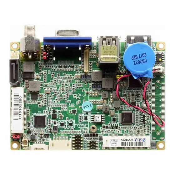
Summary of Contents for Aaeon Aaeon PICO-BT01
- Page 1 PICO-BT01 Pico-ITX Board User’s Manual 11 Last Updated: September 30, 2021...
- Page 2 AAEON assumes no liabilities resulting from errors or omissions in this document, or from the use of the information contained herein. AAEON reserves the right to make changes in the product design without notice to its users.
- Page 3 Acknowledgements All other products’ name or trademarks are properties of their respective owners. Microsoft Windows® is a registered trademark of Microsoft Corp. ⚫ Intel® and Celeron® are registered trademarks of Intel Corp. ⚫ Intel Atom™ is a trademark of Intel Corp. ⚫...
- Page 4 Packing List Before setting up your product, please make sure the following items have been shipped: Item Quantity PICO-BT01 ⚫ Heat Spreader ⚫ COM x 2, Line-out Cable ⚫ If any of these items are missing or damaged, please contact your distributor or sales representative immediately.
- Page 5 (if any), its specifications, dimensions, jumper/connector settings/definitions, and driver installation instructions (if any), to facilitate users in setting up their product. Users may refer to the product page at AAEON.com for the latest version of this document. Preface...
- Page 6 Safety Precautions Please read the following safety instructions carefully. It is advised that you keep this manual for future references All cautions and warnings on the device should be noted. Make sure the power source matches the power rating of the device. Position the power cord so that people cannot step on it.
- Page 7 If any of the following situations arises, please the contact our service personnel: Damaged power cord or plug Liquid intrusion to the device iii. Exposure to moisture Device is not working as expected or in a manner as described in this manual The device is dropped or damaged Any obvious signs of damage displayed on the device...
- Page 8 FCC Statement This device complies with Part 15 FCC Rules. Operation is subject to the following two conditions: (1) this device may not cause harmful interference, and (2) this device must accept any interference received including interference that may cause undesired operation.
- Page 9 China RoHS Requirements (CN) 产品中有毒有害物质或元素名称及含量 AAEON Main Board/ Daughter Board/ Backplane 有毒有害物质或元素 部件名称 铅 汞 镉 六价铬 多溴联苯 多溴二苯醚 (Pb) (Hg) (Cd) (Cr(VI)) (PBB) (PBDE) 印刷电路板 × ○ ○ ○ ○ ○ 及其电子组件 外部信号 × ○ ○ ○ ○ ○...
- Page 10 China RoHS Requirement (EN) Poisonous or Hazardous Substances or Elements in Products AAEON Main Board/ Daughter Board/ Backplane Poisonous or Hazardous Substances or Elements Hexavalent Polybrominated Polybrominated Component Lead Mercury Cadmium Chromium Biphenyls Diphenyl Ethers (Pb) (Hg) (Cd) (Cr(VI)) (PBB) (PBDE) PCB &...
-
Page 11: Table Of Contents
Table of Contents Chapter 1 - Product Specifications..................1 Specifications ......................2 Chapter 2 – Hardware Information ..................5 Dimensions ....................... 6 Jumpers and Connectors ..................11 List of Jumpers ......................13 2.3.1 Clear CMOS Jumper (JP1 Pins 1,3,5) ............13 2.3.2 Auto Power Button Enable/Disable Selection (JP1 Pins 2,4,6) .... - Page 12 2.4.15 External +12V Input (CN20) ................. 26 2.4.16 Buzzer Connector (CN21) ................27 2.4.17 BIO Connector (CN22) .................. 27 2.4.18 COM Port 1, Port 2 & Line Out Connector (CN23) ......... 29 2.4.19 Mini Card Slot (Half-Size) (CN24) ..............31 2.4.20 LVDS Port (CN25) ...................
- Page 13 Setup Submenu: Boot ..................62 Setup submenu: Save & Exit ................63 Chapter 4 – Drivers Installation .................... 64 Driver Download/Installation ................65 Appendix A - I/O Information ....................67 I/O Address Map ....................68 Memory Address Map ..................69 IRQ Mapping Chart ....................
-
Page 14: Chapter 1 - Product Specifications
Chapter 1 Chapter 1 - Product Specifications... -
Page 15: Specifications
Specifications System Form Factor Pico-ITX Intel® Celeron® J1900 (4C, 2GHz, up to 2.42GHz, TDP 10W) Intel® Celeron® N2807 (2C, 1.58GHz, up to 2.16GHz, TDP 4.3W) Intel Atom® E3845 (4C, 1.91GHz, TDP 10W) Intel Atom® E3825 (2C, 1.33GHz, TDP 6W) CPU Frequency Up to 2.42GHz Chipset Onboard Intel Atom®... - Page 16 System Storage Temperature -40°F ~ 176°F (-40°C ~ 80°C) Operating Humidity 0% ~ 90% relative humidity, non-condensing MTBF (Hours) 80,000 Certification CE, FCC OS Support Windows 10 (64 bit) Windows 7 (64 bit) Ubuntu 21.04.0/Kernel 5.10 Display Onboard Intel Atom® E3845/E3825, and Chipset Celeron®...
- Page 17 4-bit (2-in, 2-out) Expansion Slot Mini Card (Half-size) x 1 BIO x 1 Option by BIO Board — Chapter 1 – Product Specifications...
-
Page 18: Chapter 2 - Hardware Information
Chapter 2 Chapter 2 – Hardware Information... -
Page 19: Dimensions
Dimensions Component Side Chapter 2 – Hardware Information... - Page 20 Solder Side Chapter 2 – Hardware Information...
- Page 21 Heat Spreader Chapter 2 – Hardware Information...
- Page 22 Chapter 2 – Hardware Information...
- Page 23 Chapter 2 – Hardware Information...
-
Page 24: Jumpers And Connectors
Jumpers and Connectors Component Side Chapter 2 – Hardware Information... - Page 25 Chapter 2 – Hardware Information...
-
Page 26: List Of Jumpers
List of Jumpers Please refer to the table below for all of the board’s jumpers that you can configure for your application Label Function JP1 (Pins 1,3,5) Clear CMOS Jumper JP1 (Pins 2,4,6) Auto Power Button Enable/Disable Selection LVDS Port Operating Voltage Selection JP4 (Pins 1,3,5) LVDS Port Backlight Inverter Voltage Selection JP4 (Pins 2,4,6) -
Page 27: Lvds Port Operating Voltage Selection (Jp3)
2.3.3 LVDS Port Operating Voltage Selection (JP3) +3.3V (Default) 2.3.4 LVDS Port Backlight Inverter Voltage Selection (JP4 Pins 1,3,5) +12V +5V (Default) 2.3.5 LVDS Port Backlight Lightness Control Mode Selection (JP4 Pins 2,4,6) VR Mode (Defalt) PWM Mode Note: To prevent damage to the system or unwanted operation, do not use any other configuration for JP4 than what is shown in Ch 2.3.4 and Ch 2.3.5. -
Page 28: List Of Connectors
List of Connectors Please refer to the table below for all of the board’s connectors that you can configure for your application Label Function Battery DDR3L SO-DIMM Slot VGA Port DP port LVDS Port Inverter / Backlight Connector LAN (RJ-45) Port Digital IO Port Mini Card Slot (Full Size)/ Default mSATA (feature select by BOM) CN10... -
Page 29: Battery (Cn1)
2.4.1 Battery (CN1) Pin Name Signal Type Signal Level +3.3V 3.3V 2.4.2 DDR3L SO-DIMM Slot (CN2) Standard specifications 2.4.3 VGA Port (CN3) Pin Name Signal Type Signal Level GREEN BLUE RED_GND_RTN GREEN_GND_RTN BLUE_GND_RTN DDC_DATA Chapter 2 – Hardware Information... -
Page 30: Dp Port (Cn4)
Pin Name Signal Type Signal Level HSYNC VSYNC DDC_CLK 2.4.4 DP Port (CN4) Pin Name Signal Type Signal Level DDI0_DP_D0_P DIFF DDI0_DP_D0_N DIFF DDI0_DP_D1_P DIFF DDI0_DP_D1_N DIFF DDI0_DP_D2_P DIFF DDI0_DP_D2_N DIFF DDI0_DP_D3_P DIFF DDI0_DP_D3_N DIFF DDI0_DP_AUX_P +3.3V Chapter 2 – Hardware Information... -
Page 31: Lvds Port Inverter / Backlight Connector (Cn5)
Pin Name Signal Type Signal Level DDI0_DP_AUX_N +3.3V HPLG_DETECT +1.8V RTN_PWR +3.3V 2.4.5 LVDS Port Inverter / Backlight Connector (CN5) Pin Name Signal Type Signal Level BKL_PWR +5V / +12V BKL_CONTROL BKL_ENABLE +3.3V Note 1: LVDS2/BKL_PWR can be set to +5V or +12V by JP4 (Pins 1,3,5). Note 2: LVDS2/BKL_CONTROL can be set by JP4 (Pins 2,4,6). -
Page 32: Lan (Rj-45) Port (Cn7)
2.4.6 LAN (RJ-45) Port (CN7) Pin Name Signal Type Signal Level MDI0+ DIFF MDI0- DIFF MDI1+ DIFF MDI2+ DIFF MDI2- DIFF MDI1- DIFF MDI3+ DIFF MDI3- DIFF 2.4.7 Digital IO Port (CN8) Pin Name Signal Type Signal Level DIO0 DIO1 DIO2 DIO3 Chapter 2 –... -
Page 33: Full-Size Mini Card/ Msata Slot (Cn9)
2.4.8 Full-Size Mini Card/ mSATA Slot (CN9) Pin Name Signal Type Signal Level PCIE_WAKE# +3.3VSB/+3.3V +3.3V +1.5V +1.5V PCIE_CLK_REQ# UIM_PWR UIM_DATA PCIE_REF_CLK- DIFF UIM_CLK PCIE_REF_CLK+ DIFF UIM_RST UIM_VPP W_DISABLE# +3.3V PCIE_RST# +3.3V PCIE_RX-/mSATARX+ DIFF +3.3VSB/+3.3V +3.3V Chapter 2 – Hardware Information... - Page 34 Pin Name Signal Type Signal Level PCIE_RX+/mSATARX- DIFF +1.5V +1.5V SMB_CLK +3.3V PCIE_TX-/mSATATX- DIFF SMB_DATA +3.3V PCIE_TX+/mSATATX+ DIFF USB_D- DIFF USB_D+ DIFF +3.3VSB/+3.3V +3.3V +3.3VSB/+3.3V +3.3V +1.5V +1.5V Chapter 2 – Hardware Information...
-
Page 35: Usb Ports 0 And 1 (Cn10)
Pin Name Signal Type Signal Level +3.3VSB/+3.3V +3.3V 2.4.9 USB Ports 0 and 1 (CN10) Note: Only Port 0 supports USB3.2 Gen 1 Pin Name Signal Type Signal Level +5VSB USB0_D- DIFF USB0_D+ DIFF USB0_SSRX− DIFF USB0_SSRX+ DIFF USB0_SSTX− DIFF USB0_SSTX+ DIFF +5VSB... -
Page 36: Usb 2.0 Port 2 (Cn11)
2.4.10 USB 2.0 Port 2 (CN11) Pin Name Signal Type Signal Level +5VSB USB2_D- DIFF USB2_D+ DIFF 2.4.11 +5V Output for SATA HDD (CN14) Pin Name Signal Type Signal Level Chapter 2 – Hardware Information... -
Page 37: Sata Port (Cn15)
2.4.12 SATA Port (CN15) Pin Name Signal Type Signal Level SATA_TX1+ DIFF SATA_TX1- DIFF SATA_RX1- DIFF SATA_RX1+ DIFF Chapter 2 – Hardware Information... -
Page 38: Lpc Port (Cn18)
2.4.13 LPC Port (CN18) Pin Name Signal Type Signal Level LAD0 +3.3V LAD1 +3.3V LAD2 +3.3V LAD3 +3.3V +3.3V +3.3V LFRAME# LRESET# +3.3V LCLK SMB_DATA [Default] / I2C_DATA SMB_CLK [Default] / I2C_CLK SMB_ALERT [Default] / +3.3V INT_SERIRQ Chapter 2 – Hardware Information... -
Page 39: Front Panel (Cn19)
2.4.14 Front Panel (CN19) Pin Name Pin Name PWR_BTN- PWR_BTN+ HDD_LED- HDD_LED+ BUZZER- BUZZER+ PWR_LED- PWR_LED+ H/W RESET- H/W RESET+ 2.4.15 External +12V Input (CN20) Pin Name Signal Type Signal Level +12V +12V Chapter 2 – Hardware Information... -
Page 40: Buzzer Connector (Cn21)
2.4.16 Buzzer Connector (CN21) Pin Name Signal Type Signal Level +3.3V 3.3V BUZZER- 2.4.17 BIO Connector (CN22) Pin Name Pin Name +12VSB PCIE_TXN0 PCIE_RXN0 PCIE_TXP0 PCIE_RXP0 PS_ON# +5VSB +5VSB +5VSB +5VSB PCIE_REF_CLK0 RESET# PCIE_REF_CLK0# Chapter 2 – Hardware Information... - Page 41 Pin Name Pin Name USBN0 USBP0 USBN1 USBP2 I2C_CLK or SMB_CLK [Default] I2C_DATA or SMB_DATA [Default] WAKE# USB_OC0# USB_OC1# LPC_AD0 LPC_FRAME# LPC_AD1 SERIRQ LPC_AD2 LPC_DRQ LPC_AD3 PWR_OK/GPIO AGND LPC_CLK AUD_LINEOUT_L PME# AUD_LINEOUT_R Chapter 2 – Hardware Information...
-
Page 42: Com Port 1, Port 2 & Line Out Connector (Cn23)
2.4.18 COM Port 1, Port 2 & Line Out Connector (CN23) Pin Name Signal Type Signal Level DCDB DSRB RTSB ±9V ±9V CTSB DTRB ±9V RIB/+5V/+12V IN/ PWR +5V/+12V DCDA DSRA RTSA ±9V ±9V CTSA DTRA ±9V AGND LOUT_R LOUT_L Chapter 2 –... - Page 43 COM Port 2 RS-485 Pin Name Signal Type Signal Level RS485_D- ±5V RS485_D+ ±5V NC/+5V/+12V +5V/+12V COM Port 2 RS-422 Pin Name Signal Type Signal Level RS422_TX- ±5V RS422_TX+ ±5V RS422_RX+ RS422_RX- NC/+5V/+12V +5V/+12V Note 1: COM2 RS-232/422/485 can be set by BIOS setting. Default is RS-232. Note 2: COM2 RI/ +5V/ +12V function can be set by BOM (R524 RI/ R521 +12V/ R526 +5V) Chapter 2 –...
-
Page 44: Mini Card Slot (Half-Size) (Cn24)
2.4.19 Mini Card Slot (Half-Size) (CN24) Pin Name Signal Type Signal Level PCIE_WAKE# +3.3VSB +3.3V +1.5V +1.5V PCIE_CLK_REQ# PCIE_REF_CLK- DIFF PCIE_REF_CLK+ DIFF W_DISABLE# +3.3V PCIE_RST# +3.3V PCIE_RX- DIFF +3.3VSB +3.3V Chapter 2 – Hardware Information... - Page 45 Pin Name Signal Type Signal Level PCIE_RX+ DIFF +1.5V +1.5V SMB_CLK +3.3V PCIE_TX- DIFF SMB_DATA +3.3V PCIE_TX+ DIFF USB_D- DIFF USB_D+ DIFF +3.3VSB +3.3V +3.3VSB +3.3V +1.5V +1.5V Chapter 2 – Hardware Information...
-
Page 46: Lvds Port (Cn25)
Pin Name Signal Type Signal Level +3.3VSB +3.3V 2.4.20 LVDS Port (CN25) Pin Name Signal Type Signal Level BKL_ENABLE BKL_CONTROL LCD_PWR +3.3V/+5V LVDS_A_CLK- DIFF LVDS_A_CLK+ DIFF LCD_PWR +3.3V/+5V LVDS_DA0+ DIFF LVDS_DA0- DIFF LCD_PWR +3.3V/+5V LVDS_DA1+ DIFF LVDS_DA1- DIFF LVDS_DA2+ DIFF LVDS_DA2- DIFF LVDS_DA3+... - Page 47 Pin Name Signal Type Signal Level LVDS_DA3- DIFF DDC_DATA DDC_CLK Chapter 2 – Hardware Information...
-
Page 48: Chapter 3 - Ami Bios Setup
Chapter 3 Chapter 3 - AMI BIOS Setup... -
Page 49: System Test And Initialization
System Test and Initialization The board uses certain routines to perform testing and initialization. If an error, fatal or non-fatal, is encountered, a few short beeps or an error message will be outputted. The board can usually continue the boot up sequence with non-fatal errors. The system configuration verification routines check the current system configuration against the values stored in the CMOS memory. -
Page 50: Ami Bios Setup
AMI BIOS Setup The AMI BIOS ROM has a pre-installed Setup program that allows users to modify basic system configurations, which is stored in the battery-backed CMOS RAM and BIOS NVRAM so that the information is retained when the power is turned off. To enter BIOS Setup, press <Del>... -
Page 51: Setup Submenu: Main
Setup Submenu: Main Press “Delete” to enter Setup Chapter 3 – AMI BIOS Setup... -
Page 52: Setup Submenu: Advanced
Setup Submenu: Advanced Chapter 3 – AMI BIOS Setup... -
Page 53: Advanced: Acpi Settings
3.4.1 Advanced: ACPI Settings Options summary: ACPI Sleep State Suspend Disabled Optimal Default, Failsafe Default S3 (suspend to RAM) Select the highest ACPI sleep state the system will enter when the SUSPEND button is pressed. Restore on Power Loss Power Off Power On Optimal Default, Failsafe Default Last State... - Page 54 Wake on Ring Disabled Optimal Default, Failsafe Default Enabled Enable or disable System Wake on Ring RTC wake system from S5 Disabled Optimal Default, Failsafe Default Fixed Time Enable or disable System wake on alarm event. When enabled, System will wake on the hr::min::sec specified Chapter 3 –...
-
Page 55: Advanced: F81801 Super Io Configuration
3.4.2 Advanced: F81801 Super IO Configuration Chapter 3 – AMI BIOS Setup... -
Page 56: Super Io Configuration: Serial Port 1 Configuration
3.4.2.1 Super IO Configuration: Serial Port 1 Configuration Chapter 3 – AMI BIOS Setup... -
Page 57: Super Io Configuration: Serial Port 2 Configuration
3.4.2.2 Super IO Configuration: Serial Port 2 Configuration Options summary: Serial Port Disabled Enabled Default Allows BIOS to En/Disable correspond serial port. Change Settings Auto Default (Serial Port 1) IO=3F8h; IRQ=4; IO=3F8h; IRQ=3,4,5,6,7,9,10,11,12; IO=2F8h; IRQ=3,4,5,6,7,9,10,11,12; Chapter 3 – AMI BIOS Setup... - Page 58 IO=3E8h; IRQ=3,4,5,6,7,9,10,11,12; IO=2E8h; IRQ=3,4,5,6,7,9,10,11,12; Allows BIOS to Select Serial Port resource. Change Settings Auto Default (Serial Port 2) IO=2F8h; IRQ=3; IO=3F8h; IRQ=3,4,5,6,7,9,10,11,12; IO=2F8h; IRQ=3,4,5,6,7,9,10,11,12; IO=3E8h; IRQ=3,4,5,6,7,9,10,11,12; IO=2E8h; IRQ=3,4,5,6,7,9,10,11,12; COM2 Type Select RS232 Default RS422 RS485 Select Working model Chapter 3 – AMI BIOS Setup...
-
Page 59: Advanced: Hardware Monitor
3.4.3 Advanced: Hardware Monitor Chapter 3 – AMI BIOS Setup... -
Page 60: Advanced: Cpu Configuration
3.4.4 Advanced: CPU Configuration Options summary: Intel Virtualization Disabled Technology Enabled Optimal Default, Failsafe Default When enabled, a VMM can utilize the additional hardware capabilities provided by Vander pool Technology Chapter 3 – AMI BIOS Setup... -
Page 61: Cpu Configuration: Socket 0 Cpu Information
3.4.4.1 CPU Configuration: Socket 0 CPU Information Chapter 3 – AMI BIOS Setup... -
Page 62: Advanced: Sata Configuration
3.4.5 Advanced: SATA Configuration Options summary: Serial-ATA (SATA) Enabled Default Disabled En/Disable SATA SATA Speed Support Gen1 Default Gen2 SATA Speed Support Gen1 or Gen2 SATA Mode Default AHCI IDE: Configure SATA controllers as legacy IDE AHCI: Configure SATA controllers to operate in AHCI mode Chapter 3 –... - Page 63 Serial-ATA Port x Enabled Default Disabled En/Disable SATA Port SATA Port1 HotPlug Enabled Disabled Default En/Disable SATA Port Hotplug Chapter 3 – AMI BIOS Setup...
-
Page 64: Advanced: Dynamic Digital Io Configuration
3.4.6 Advanced: Dynamic Digital IO Configuration Digital Port X Direction Input Output Set DIO as input or Output Digital Port X Level Default Set DIO Output port Hi or Low Chapter 3 – AMI BIOS Setup... -
Page 65: Advanced: Usb Configuration
3.4.7 Advanced: USB Configuration Options summary: Legacy USB Support Enabled Optimal Default, Failsafe Default Disabled Auto Enables BIOS Support for Legacy USB Support. When enabled, USB can be functional in legacy environment like DOS. AUTO option disables legacy support if no USB devices are connected Device Name (Emulation Auto Optimal Default, Failsafe Default... - Page 66 CDROM If Auto. USB devices less than 530MB will be emulated as Floppy and remaining as Floppy and remaining as hard drive. Forced FDD option can be used to force a HDD formatted drive to boot as FDD(Ex. ZIP drive) Chapter 3 –...
-
Page 67: Setup Submenu: Chipset
Setup Submenu: Chipset Chapter 3 – AMI BIOS Setup... -
Page 68: Chipset: North Bridge
3.5.1 Chipset: North Bridge Options summary: Primary IGFX Boot Display VBIOS Default Optimal Default, Failsafe Default LVDS Select the Video device LVDS1 Disabled Enabled Optimal Default, Failsafe Default En/Dis LVDS Panel Type 640x480 800x480 800x600 Chapter 3 – AMI BIOS Setup... - Page 69 1024x600 1024x768 Optimal Default, Failsafe Default 1280x768 1366x768 1440x900 Select panel type Color Depth 18Bit Optimal Default, Failsafe Default 24Bit Set color depth Backlight Type Normal Optimal Default, Failsafe Default Inverted Select backlight control signal type Backlight Level 0-100% Select backlight control level Panel Scaling Auto Optimal Default, Failsafe Default...
-
Page 70: Chipset: South Bridge
3.5.2 Chipset: South Bridge Options summary*: PCIE/mSATA Select PCIE Optimal Default, Failsafe Default mSATA PCIE/mSATA Select * PCIE/mSATA Select is available only for A1.0 version and not available for A1.1 and / or later version. Chapter 3 – AMI BIOS Setup... -
Page 71: South Bridge: Azalia Hd Audio
3.5.2.1 South Bridge: Azalia HD Audio Azalia HD Audio Disabled Enabled Optimal Default, Failsafe Default Enabling/Disabling HD Audio controller. Chapter 3 – AMI BIOS Setup... -
Page 72: South Bridge: Usb Configuration
3.5.2.2 South Bridge: USB Configuration Chapter 3 – AMI BIOS Setup... -
Page 73: South Bridge: Pci Express Configuration
3.5.2.3 South Bridge: PCI Express Configuration Options summary: PCI Express Root Port x Enabled Optimal Default, Failsafe Default Disabled Enabling/Disabling PCI Express root ports Hot Plug (Mini Card) Disabled Enabled Optimal Default, Failsafe Default Enable/ Disable PCEI hot plug. Chapter 3 – AMI BIOS Setup... -
Page 74: Setup Submenu: Security
Setup Submenu: Security Change User/Administrator Password You can set an Administrator Password or User Password. An Administrator Password must be set before you can set a User Password. The password will be required during boot up, or when the user enters the Setup utility. A User Password does not provide access to many of the features in the Setup utility. -
Page 75: Setup Submenu: Boot
Setup Submenu: Boot Options summary: Do not launch Optimal Default; Failsafe Default legacy Controls the execution of Legacy PXE OpROM Quiet Boot Disabled Enabled Default En/Disable showing boot logo. Chapter 3 – AMI BIOS Setup... -
Page 76: Setup Submenu: Save & Exit
Setup submenu: Save & Exit Chapter 3 – AMI BIOS Setup... -
Page 77: Chapter 4 - Drivers Installation
Chapter 4 Chapter 4 – Drivers Installation... -
Page 78: Driver Download/Installation
Driver Download/Installation Drivers for the PICO-BT01 can be downloaded from the product page on the AAEON website by following this link: https://www.aaeon.com/en/p/pico-itx-boards-pico-bt01 Download the driver(s) you need and follow the steps below to install them. Step 1 – Install Chipset Driver Open the Step1 - Chipset folder and open the SetupChipset.exe file... - Page 79 Step 4 – Install Audio Driver Open the Step4 - Audio folder and open the Win7_8-32_64_R273.exe file Follow the instructions Driver will be installed automatically Step 5 – Install USB3.0 Driver Open the Step5 - USB3.0 folder and open the Setup.exe file Follow the instructions Driver will be installed automatically Step 6 –...
-
Page 80: Appendix A - I/O Information
Appendix A Appendix A - I/O Information... -
Page 81: I/O Address Map
I/O Address Map Appendix A – I/O Information... -
Page 82: A.2 Memory Address Map
A.2 Memory Address Map Appendix A – I/O Information... -
Page 83: A.3 Irq Mapping Chart
A.3 IRQ Mapping Chart Appendix A – I/O Information... - Page 84 Appendix A – I/O Information...
- Page 85 Appendix A – I/O Information...
- Page 86 Appendix A – I/O Information...
- Page 87 Appendix A – I/O Information...
- Page 88 Appendix A – I/O Information...
- Page 89 Appendix A – I/O Information...
- Page 90 Appendix A – I/O Information...
- Page 91 Appendix A – I/O Information...
- Page 92 Appendix A – I/O Information...
- Page 93 Appendix A – I/O Information...
- Page 94 Appendix A – I/O Information...
-
Page 95: Appendix B - Electrical Specifications For I/O Ports
Appendix B Appendix B – Electrical Specifications for I/O Ports... -
Page 96: Electrical Specifications For I/O Ports
Electrical Specifications for I/O Ports Reference Signal Name Rate Output VGA: +5V +5V/0.5A LVDS Port Inverter / Backlight +5V/2A or +12V/2A Connector Digital IO Port D0~D3 +5V/(Open drain) +3.3VSB +3.3V/1.1A Mini-Card Slot +1.5V +1.5V/0.375A USB 3.0 Port 1 & 2 CN10 +5VSB +5VSB/1A (per channel) -
Page 97: Appendix C - Mating Connectors
Appendix C Appendix C – Mating Connectors... -
Page 98: List Of Mating Connectors And Cables
List of Mating Connectors and Cables The table notes mating connectors and available cables. Connector Function Mating Connector Available Cable P/N Label Cable Vendor Model no Battery Molex 51021-0200 Battery 175011901M Cable DDR3 204PIN SKT Transcend TS1GSK64W6H-I VGA Connector SUNBOX VGA Cable DPConnector Molex 0687830007... - Page 99 Connector Function Mating Connector Available Cable P/N Label Cable Vendor Model no CN18 LPC Port SHR-12V-S-B AAEON 1703120130 Cable CN19 Front Panel H820-2x05 Front 1701100156 Connector Panel Cable CN20 External +12V Molex 19211-0003 Power 170204010R Input cable CN21 Buzzer connector Molex...
Need help?
Do you have a question about the Aaeon PICO-BT01 and is the answer not in the manual?
Questions and answers