Table of Contents
Advertisement
Quick Links
Advertisement
Table of Contents

Related Manuals for Advantech SOM-4466


Summary of Contents for Advantech SOM-4466
- Page 1 User Manual SOM-4466 ETX Module User Manual...
- Page 2 No part of this manual may be reproduced, copied, translated or transmitted in any form or by any means without the prior written permission of Advantech Co., Ltd. Information provided in this manual is intended to be accurate and reliable. How- ever, Advantech Co., Ltd.
- Page 3 Consult the dealer or an experienced radio/TV technician for help. Technical Support and Assistance Visit the Advantech website at http://support.advantech.com where you can find the latest information about the product. Contact your distributor, sales representative, or Advantech's customer service center for technical support if you need additional assistance.
- Page 4 Before setting up the system, check that the items listed below are included and in good condition. If any item does not accord with the table, please contact your dealer immediately. One SOM-4466 ETX module One Heatspreader (1960058558N001) ...
- Page 5 The sound pressure level at the operator's position according to IEC 704-1:1982 is no more than 70 dB (A). DISCLAIMER: This set of instructions is given according to IEC 704-1. Advantech disclaims all responsibility for the accuracy of any statements contained herein.
- Page 6 Don't touch any components on the CPU card or other cards while the PC is on. Disconnect power before making any configuration changes. The sudden rush of power as you connect a jumper or install a card may damage sensitive elec- tronic components. SOM-4466 User Manual...
-
Page 7: Table Of Contents
SUSI....................3 1.2.7 Mechanical and Environmental Specification ....... 3 Functional Block Diagram ................. 4 SOM-4466 Pin Assignment............... 5 Table 1.1: Pin Assignment (A1-A100) ......... 5 Table 1.2: Pin Assignment (B1-B100) ......... 6 Table 1.3: Pin Assignment (C1-C100)......... 7 Table 1.4: Pin Assignment (D1-D100)......... 8... - Page 8 Table B.1: System I/O Ports ............58 DMA Channel Assignments ..............59 Table B.2: DMA Channel Assignments ........59 Interrupt Assignments ................60 Table B.3: Interrupt Assignments ..........60 1st MB Memory Map................61 Table B.4: 1st MB Memory Map ..........61 SOM-4466 User Manual viii...
-
Page 9: Chapter 1 General Information
Chapter General Information This chapter gives background information on the SOM-4466 ETX module. Sections include: Introduction Specification Functional Block Diagram SOM-4466 Pin Assignment... -
Page 10: Introduction
Introduction SOM-4466 is an embedded ETX module that fully complies with the ETX form factor standard. This ETX module supports AMD G Series T16R APU+A55E chipset which delivering sufficient performance with extremely low power consumption. SOM-4466 comes with extensive legacy interfaces such as PCI, ISA, and IDE, and support for both 24-bit LVDS, and 18-bit TTL panels. -
Page 11: Expansion Interface
(VBAT is optional; if remove VBAT, the RTC time will not be kept, and the par- tial bios setting will be lost.) Power Requirement: – Test condition: SOM-4466 (T16R), 4 GB DDR3 SO-DIMM, WIN XP SP3, Burn In Test V6.0 Pro. – Idle: +5 V @ 1.22 A –... -
Page 12: Functional Block Diagram
Humidity Specification: – Operating: 40 ° @ 95% relative humidity, non-condensing Storage: 60 ° – @ 95%relative humidity, non-condensing Functional Block Diagram SOM-4466 User Manual... -
Page 13: Som-4466 Pin Assignment
SOM-4466 Pin Assignment This section gives SOM-4466 pin assignment on ETX connector which compliant with ETX 3.02 pin-out definitions. More details about how to use these pins and get design references please contact to Advantech for design guide, checklist, reference schematic, and other hardware/software supports. - Page 14 Signal SD14 SD15 SD13 MASTER# SD12 DREQ7 SD11 DACK#7 SD10 DREQ6 DACK#6 DREQ5 MEMW# DACK#5 MEMR# DREQ0 LA17 DACK#0 LA18 IRQ14 LA19 IRQ15 LA20 IRQ12 LA21 IRQ11 LA22 IRQ10 LA23 IO16# SBHE# M16# BALE DACK#2 IRQ3 IRQ4 SOM-4466 User Manual...
- Page 15 DDDA DDDA LCDB0 LCDB2 C13 LCDB1 LCDB3 C15 GND C17 LCDG5 FPVSYNC C19 LCDG4 FPHSYNC C21 GND C23 LCDG0 TX03- LCDG3 C25 LCDG1 TX03+ LCDG2 C27 GND C29 LCDR4 TX02- LCDB5 TXCK0+ C31 LCDR5 TX02+ LCDB4 TXCK0- SOM-4466 User Manual...
- Page 16 SLCT# WGATE# C91 DSR1# DSR1# MSCLK MSCLK C93 CTS1# CTS1# MSDAT MSDAT C95 TXD1 TXD1 KBCLK KBCLK C97 RI1# RI1# KBDAT KBDAT C99 GND C100 GND Table 1.4: Pin Assignment (D1-D100) Signal Signal 5V_SB PWGIN PS_ON# SPEAKER SOM-4466 User Manual...
- Page 17 SIDE_D14 PIDE_D0 SIDE_D1 PIDE_D14 SIDE_D13 PIDE_D1 SIDE_D2 PIDE_D13 SIDE_D12 PIDE_D2 SIDE_D3 PIDE_D12 SIDE_D11 PIDE_D3 SIDE_D4 PIDE_D11 SIDE_D10 PIDE_D4 SIDE_D5 PIDE_D10 SIDE_D9 PIDE_D5 SIDE_D6 PIDE_D9 SIDE_D8 PIDE_D6 GPE#2 (RING#) LAN_RXD- PIDE_D8 LAN_RXD+ SIDE_D7 LAN_TXD- PIDE_D7 LAN_TXD+ HDRST# D100 SOM-4466 User Manual...
- Page 18 SOM-4466 User Manual...
-
Page 19: Chapter 2 Mechanical Information
Chapter Mechanical Information This chapter gives mechanical information on the SOM-4466 ETX module. Sections include: Board Information Mechanical Drawing... -
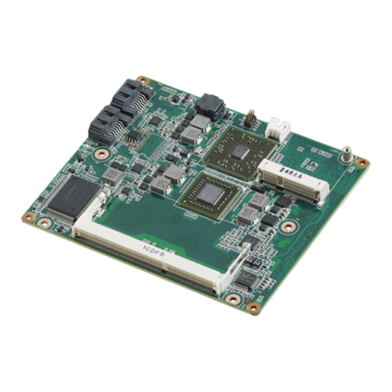
Page 20: Board Information
Board Information The figures below indicate the main chips on SOM-4466 ETX 3.02 module. Please be aware of these positions while designing the customer's own carrier board to avoid mechanical and thermal problems. BIOS Socket mSATA AMD FCH A55E Socket... -
Page 21: Mechanical Drawing
Mechanical Drawing For more details about 2D/3D models, please refer to Advantech’s COM support ser- vice website http://com.advantech.com. Figure 2.3 Board Mechanical Drawing - Front Figure 2.4 Board Mechanical Drawing - Back SOM-4466 User Manual... - Page 22 SOM-4466 User Manual...
-
Page 23: Chapter 3 Ami Bios
Chapter AMI BIOS Sections include: Introduction Entering Setup... -
Page 24: Introduction
AMI BIOS has been integrated into many motherboards for over a decade. With the AMI BIOS Setup program, users can modify BIOS settings and control various sys- tem features. This chapter describes the basic navigation of the SOM-4466 BIOS setup screens. -
Page 25: Entering Setup
System Date using the <Arrow> keys. Enter new values through the keyboard. Press the <Tab> key or the <Arrow> keys to move between fields. The date must be entered in MM/DD/YY format. The time must be entered in HH:MM:SS format. SOM-4466 User Manual... -
Page 26: Advanced Bios Features Setup
3.2.2 Advanced BIOS Features Setup Select the Advanced tab from the SOM-4466 setup screen to enter the Advanced BIOS Setup screen. Users can select any item in the left frame of the screen, such as CPU Configuration, to go to the sub menu for that item. Users can display an Advanced BIOS Setup option by highlighting it using the <Arrow>... - Page 27 3.2.2.1 PCI Bus Driver Version Figure 3.4 PCI Bus Driver Version PCI ROM Priority This item allows users to choose the priority. SOM-4466 User Manual...
- Page 28 This item allows users to enable or disable BIOS ACPI auto configuration. Enable Hibernation This item allows users to enable or disable hibernation. ACPI Sleep State This item allows users to set the ACPI sleep state. SOM-4466 User Manual...
- Page 29 This item allows users to enable or disable PSS support. PSTATE Adjustment This item provides to adjust startup P-state level. PPC Adjustment This item provides to adjust PPC object. C6 mode This item allows users to enable or disable C6 mode. SOM-4466 User Manual...
- Page 30 Node 0 Information Figure 3.7 Node 0 Information – Node 0 Information View memory information related to Node 0 SOM-4466 User Manual...
- Page 31 3.2.2.4 IDE Configuration Figure 3.8 IDE Configuration IDE Support IDE default setting is closed. *If this function is enabled and no device is attached, the boot time will be longer. SOM-4466 User Manual...
- Page 32 Host Controller. 'Auto' uses default value: for a Root port it is 100 ms, for a Hub port the delay is taken from Hub descriptor. Mass Storage Devices USB 2.0 Flash Disk 0. uses "Auto" as default value. SOM-4466 User Manual...
- Page 33 This item allows users to enable or disable Watch Dog timer. FDC and LPT Select This item default is "Parallel Port". Change settings default is "Auto" and Device Mode default is "ECP and EPP 1.9 Mode". SOM-4466 User Manual...
- Page 34 Floppy Disk Controller Configuration Figure 3.11 Floppy Disk Controller Configuration – Floppy Disk Controller This item allows users to enable or disable Floppy Disk Controller. SOM-4466 User Manual...
- Page 35 Serial Port 1 Configuration Figure 3.12 Serial Port 1 Configuration – Serial Port This item allows users to enable or disable Serial port 1. – Change settings Serial port 1 IRQ/IO/mode resources configuration. Users can choose IRQ,IO, and MODE. SOM-4466 User Manual...
- Page 36 – Serial Port This item allows users to enable or disable Serial port 2. – Change settings Serial port 2 IRQ/IO/mode resources configuration. Users can choose IRQ,IO, and MODE. – Device Mode Users can choose the mode. SOM-4466 User Manual...
- Page 37 Figure 3.14 Parallel Port Configuration – Parallel Port This item allows users to enable or disable. – Change Setting This item allows users to change settings. – Device Mode This item allows users to change the mode. SOM-4466 User Manual...
- Page 38 Super IO 2 Configuration Figure 3.15 Super IO 2 Configuration Serial Port 3 Configuration This item allows users to configure serial port 3. Serial Port 4 Configuration This item allows users to configure serial port 4. SOM-4466 User Manual...
- Page 39 Serial Port 3 Configuration Figure 3.16 Serial Port 3 Configuration – Serial Port This item allows users to enable or disable Serial port 3. SOM-4466 User Manual...
- Page 40 Serial Port 4 Configuration Figure 3.17 Serial Port 4 Configuration – Serial Port This item allows users to enable or disable Serial port 4. SOM-4466 User Manual...
- Page 41 Parallel Port 2 Configuration This item allows users to configure parallel port. Figure 3.18 Parallel Port 2 Configuration – Parallel Port 2 This item allows users to enable or disable Parallel Port 2. SOM-4466 User Manual...
- Page 42 3.2.2.8 H/W Monitor Figure 3.19 H/W Monitor ACPI Critical Shutdown This item allows users to enable or disable ACPI Critical shutdown. SOM-4466 User Manual...
- Page 43 Figure 3.20 IT8888 Configuration IT8888 ISA Decode This item allows users to select the decode mode. Memory Hole 15 MB - 16 MB This item allows users to enable or disable Memory Hole 15 MB - 16 MB. SOM-4466 User Manual...
- Page 44 This item allows users to enable or disable DDMA Slave Channel 5. – DDMA Slave Channel 6 This item allows users to enable or disable DDMA Slave Channel 6. – DDMA Slave Channel 7 This item allows users to enable or disable DDMA Slave Channel 7. SOM-4466 User Manual...
-
Page 45: Chipset
Setup screen. You can display a Chipset BIOS Setup option by highlighting it using the <Arrow> keys. All Plug and Play BIOS Setup options are described in this sec- tion. The Plug and Play BIOS Setup screen is shown below. Figure 3.22 Chipset Setup SOM-4466 User Manual... - Page 46 3.2.3.1 North Bridge Configuration Figure 3.23 North Bridge Configuration Memory Configuration This item allows users to enable or disable Integrated Graphics. Socket 0 Information This item is shown the socket 0 information. SOM-4466 User Manual...
- Page 47 Memory Configuration Figure 3.24 Memory Configuration – Integrated Graphics This item allows users to enable or disable Integrated Graphics. SOM-4466 User Manual...
- Page 48 Socket 0 Information Figure 3.25 Socket 0 Information – Socket 0 Information This item is shown the socket 0 information. SOM-4466 User Manual...
- Page 49 3.2.3.2 North Bridge LCD Config Select (LVDS SKU) Figure 3.26 North Bridge LCD Config Select (LVDS SKU) LVDS Output Mode This item allows users to enable or disable LVDS Output mode. SOM-4466 User Manual...
- Page 50 3.2.3.3 North Bridge LCD Config Select (TTL SKU) Figure 3.27 North Bridge LCD Config Select (TTL SKU) TTL Output Mode This item allows users to enable or disable TTL Output mode. SOM-4466 User Manual...
- Page 51 Figure 3.28 South Bridge HD Audio Azalia Device This item allows users to enable or disable HD Audio Azalia Device. On Board Network Cont This item allows users to enable or disable On Board Network Cont. SOM-4466 User Manual...
- Page 52 This item allows users to enable or disable SATA Power on mSATA. – IDE Power on Secondary This item allows users to enable or power down IDE Power on Secondary. – IDE Power on Primary This item allows users to enable or power down IDE Power on Primary. SOM-4466 User Manual...
- Page 53 This item allows users to enable or disable USB Port 1. – USB PORT 2 This item allows users to enable or disable USB Port 2. – USB PORT 3 This item allows users to enable or disable USB Port 3. SOM-4466 User Manual...
-
Page 54: Boot Settings
If this option is set to Disabled, the BIOS displays normal POST messages. If Enabled, an OEM Logo is shown instead of POST messages. Fast Boot This option is set to Disabled. 1st/2nd/3rd Boot This item allows users to set boot device priority. SOM-4466 User Manual... -
Page 55: Security Setup
Security Setup Figure 3.32 Password Configuration Select Security Setup from the SOM-4466 Setup main BIOS setup menu. All Security Setup options, such as password protection is described in this section. To access the sub menu for the following items, select the item and press <Enter>: ... -
Page 56: Save & Exit
Restore Defaults The SOM-4466 automatically configures all setup items to optimal settings when users select this option. Optimal Defaults are designed for maximum sys- tem performance, but may not work best for all computer applications. In partic- ular, do not use the Optimal Defaults if the user's computer is experiencing system configuration problems. - Page 57 Save User Defaults When users have completed system configuration, select this option to save changes as user defaults without exit BIOS setup menu. Restore User Defaults The users can select this option to restore user defaults. SOM-4466 User Manual...
- Page 58 SOM-4466 User Manual...
-
Page 59: Installation
Chapter S/W Introduction & Installation Sections include: S/W Introduction Driver Installation... -
Page 60: S/W Introduction
S/W Introduction The mission of Advantech Embedded Software Services is to "Enhance quality of life with Advantech platforms and Microsoft Windows embedded technology." We enable Windows Embedded software products on Advantech platforms to more effectively support the embedded computing community. Customers are freed from the hassle of dealing with multiple vendors (Hardware suppliers, System integrators, Embedded OS distributor) for projects. -
Page 61: Watchdog Timer
Appendix Watchdog Timer This appendix gives you the infor- mation about the watchdog timer programming on the SOM-4466 ETX module. Sections include: Watchdog Timer Programming... -
Page 62: Programming The Watchdog Timer
MOV AL,F5H; Setting counter unit is second OUT DX,AL MOV DX,2FH MOV AL,00H OUT DX,AL; MOV DX,2EH MOV AL,F6H OUT DX,AL MOV DX,2FH MOV AL,05H; Set 5 seconds OUT DX,AL ;------------------------------------------------------------- ; Exit extended function mode | ;------------------------------------------------------------- MOV DX,2EH MOV AL,AAH SOM-4466 User Manual... - Page 63 OUT DX,AL SOM-4466 User Manual...
- Page 64 SOM-4466 User Manual...
-
Page 65: System Assignments
Appendix System Assignments This appendix gives you the infor- mation about the system resource allocation on the SOM-4466 ETX module. Sections include: System I/O Ports DMA Channel Assignments Interrupt Assignments 1st MB Memory Map... -
Page 66: System I/O Ports
03E0 - 0CF7 PCI bus 03F6 - 03F6 Primary IDE Channel 03F8 - 03FF Communications Port (COM1) 040B - 040B Motherboard resources 04D0 - 04D1 Motherboard resources 04D6 - 04D6 Motherboard resources 0800 - 089F Motherboard resources SOM-4466 User Manual... -
Page 67: Dma Channel Assignments
F140 - F147 Standard Dual Channel PCI IDE Controller F150 - F15F Standard Dual Channel PCI IDE Controller FE00 - FEFE Motherboard resources DMA Channel Assignments Table B.2: DMA Channel Assignments Channel Function Direct memory access controller SOM-4466 User Manual... -
Page 68: Interrupt Assignments
Standard Enhanced PCI to USB Host Controller IRQ 18 AMD Radeon HD 6250 Graphics IRQ 18 Standard OpenHCD USB Host Controller IRQ 18 Standard OpenHCD USB Host Controller IRQ 19 Microsoft UAA Bus Driver for High Definition Audio SOM-4466 User Manual... -
Page 69: 1St Mb Memory Map
Standard OpenHCD USB Host Controller FEB4C000-FEB4C3FF Standard Dual Channel PCI IDE Controller FEC00000-FEC00FFF Motherboard resources FEC1000-FEC10FFF Motherboard resources FED0000-FED003FF High precision event timer FED0000-FED00FFF Motherboard resources FED6100-FED70FFF Motherboard resources FED8000-FED8FFFF Motherboard resources FEE0000-FEE00FFF Motherboard resources FEC0000-FFFFFFFF Motherboard resources SOM-4466 User Manual... - Page 70 No part of this publication may be reproduced in any form or by any means, electronic, photocopying, recording or otherwise, without prior written permis- sion of the publisher. All brand and product names are trademarks or registered trademarks of their respective companies. © Advantech Co., Ltd. 2013...
Need help?
Do you have a question about the SOM-4466 and is the answer not in the manual?
Questions and answers