Table of Contents
Advertisement
Quick Links
Advertisement
Table of Contents

Related Manuals for Icop VDX-6326RD-NF


Summary of Contents for Icop VDX-6326RD-NF
- Page 1 User Manual VDX-6326RD-NF with DM&P Vortex86DX 800MHz processor Version 1.1...
- Page 2 No part of this manual may be reproduced, copied, translated or transmitted, in whole or in part, in any form or by any means without the prior to written permission of ICOP Technology Inc. ⓒ Copyright 2018 ICOP Technology Inc Trademarks Acknowledgement Vortex86DX is the registered trademark of DM&P Electronics Inc.
- Page 3 VDX-6326RD-NF User Manual Revision History Revision Date Remark May 7, 2017 First version released Feb 7, 2020 Remove Y cable from cable list ICOP Technology Inc.
-
Page 4: Table Of Contents
J12: COM2 RS232/433/485 (Optional: TTL) ................10 J15: RS485 (Auto direction) ......................11 J16: Power Connector (Terminal Block: 5.0mm) ................ 11 J17: COM3 (Optional: TTL) ......................11 J18: Parallel ............................12 J19: COM4 (Optional: TTL) ......................12 ICOP Technology Inc. - Page 5 2.9 PWM ..............................25 2.10IDE to Micro SD .......................... 26 Driver Installation ........................... 27 Software Resources......................... 28 4.1 ICOP Technical Resource Website ..................... 28 Technical Support Directly from ICOP ....................29 User Manual Feedback ..........................29 Appendix ..............................30 TFT Flash Panel Data Output ......................30...
- Page 6 User Manual TFT Flash Panel Support List ......................31 Flat Panel Hardware Setting ........................ 33 Flat Panel Wiring and Lighting ......................34 TCP/IP Library for DOS Real Mode....................34 BIOS Default Setting ........................... 35 Warranty ..............................36 ICOP Technology Inc.
-
Page 7: General Information
VDX-6326RD-NF User Manual General Information 1.1 Packing List Product Name Package VDX-6326RD-NF board x1 LAN cable x2 VDX-6326RD-NF RS232 cable x3 GPIO cable x1 VDX-6326RD-NF-512 Parallel cable x1 Audio line x2 IDE cable x1 USB cable x1 1.2 Block diagram... -
Page 8: Specifications
9-pin D-Sub male connector for RS232 x1 15-pin D-Sub female connector for VGA x1 RJ45 connector for Ethernet x1 USB connector x1 Mini DIN connector for Keyboard/Mouse x1 Type I/II Compact Flash Slot x1 PCI-104 connector x1 (Optional) ICOP Technology Inc. -
Page 9: Ordering Information
VxWorks 1.4 Ordering Information PART NO. VDX-6326RD-NF VDX-6326RD-NF-512 CPU (MHz) 800MHz DRAM (DDR3) 256MB 512MB IDE DoM Storage Compact Flash SPI Flash Display VGA, LVDS, TFT-LCD PC/104, PCI-104 (Optional) RS232 RS485 Parallel Audio Line-out, MIC-in Keyboard Mouse ICOP Technology Inc. -
Page 10: Hardware Information
VDX-6326RD-NF User Manual 2 Hardware Information 2.1 Dimension ICOP Technology Inc. -
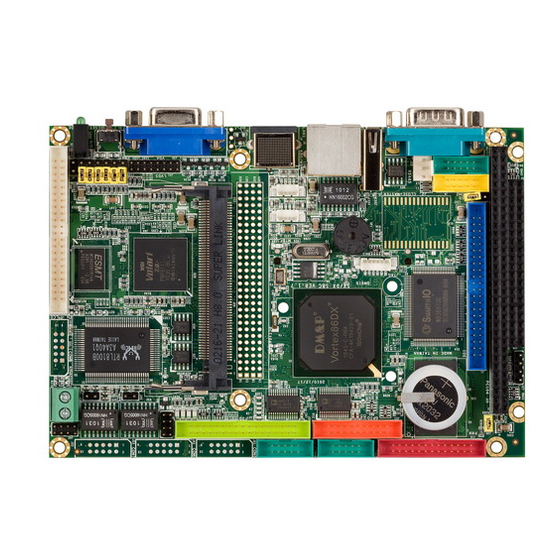
Page 11: Board Outline And Connector Location
VDX-6326RD-NF User Manual 2.2 Board Outline and Connector Location Note: 1. COM2 RS232/422/485 is selected by BIOS setting. 2. PCI-104 connector is optional. 3. VI/O default setting of PCI-104 connector is +5V 4. VDX-6326RD-NF-512 is optional. ICOP Technology Inc. -
Page 12: Connector And Jumper Summary
Box Header, 2.0mm, 30x4 D-Sub Female Connector LVDS Pin Header, 2.0mm, 8x2 J32 to Jumper Switch for Pin Header, 2.54mm, 3x1 Display Type Box Header, 2.0mm, 22x2 Line-out Wafer, 1.25mm, 4x1 MIC-in Wafer, 1.25mm, 4x1 LAN2 Pin Header, 2.00mm, 2x4 ICOP Technology Inc. - Page 13 Jumper Switch for LAN2 Pin Header, 2.54mm, 2x1 Jumper Switch for LAN3 Pin Header, 2.54mm, 2x1 Compact Flash Type I/II CF Slot Power Active LED (Red) IDE Active (Green) MTBF MTBF LED (Orange) LED SMD Buzzer Reset Switch ICOP Technology Inc.
-
Page 14: Pin Assignments & Jumper Settings
IDED10 IDED4 IDED11 IDED3 IDED12 IDED2 IDED13 IDED1 IDED14 IDED0 IDED15 IDEREQ IDEIOW IDEIOR ICHRDY IDEACK IDEINT IDESA1 IDECBLID IDESA0 IDESA2 IDECS-0 IDECS1 IDELED J2: Jumper Switch for CF Mater/Slave Pin# Signal Name CLOSE Master OPEN Slave ICOP Technology Inc. -
Page 15: J4: Usb1
J6: LAN Pin# Signal Name Pin # Signal Name J8: Reset Pin# Signal Name Pin # Signal Name Reset J9: PS/2 Connector (for Keyboard/Mouse) Pin# Signal Name Pin # Signal Name KBCLK MSCLK KBDAT MSDAT GGND GGND GGND ICOP Technology Inc. -
Page 16: J10: Com1 (Optional: Ttl/Gpio-P4/Pwm X8)
GP12 GP03 GP13 GP04 GP14 GP05 GP15 GP06 GP16 GP07 GP17 J12: COM2 RS232/433/485 (Optional: TTL) Pin# Signal Name Pin # Signal Name DCD2/ 422TX-/ RS485- RXD2/ 422TX+/ RS485+ TXD2/ 422RX+ DTR2 / 422RX- DSR2 RTS2 CTS2 ICOP Technology Inc. -
Page 17: J15: Rs485 (Auto Direction)
User Manual J15: RS485 (Auto direction) Pin# Signal Name RS485+ RS485- J16: Power Connector (Terminal Block: 5.0mm) Pin# Signal Name J17: COM3 (Optional: TTL) Pin# Signal Name Pin # Signal Name DCD3 RXD3 TXD3 DTR3 DSR3 RTS3 CTS3 ICOP Technology Inc. -
Page 18: J18: Parallel
User Manual J18: Parallel Pin# Signal Name Pin # Signal Name STB- AFD- ERR- INIT- SLIN- ACK- BUSY SLCT J19: COM4 (Optional: TTL) Pin# Signal Name Pin # Signal Name DCD4 RXD4 TXD4 DTR4 DSR4 RTS4 CTS4 ICOP Technology Inc. -
Page 19: J25: Pc/104 Connector (64Pins)
Pin # Signal Name IOCHCHK* RESETDRV IRQ9 DRQ2 -12V +12V IOCHRDY SMEMW* SA19 SMEMR* SA18 IOW* SA17 IOR* SA16 DACK3* SA15 DRQ3* SA14 DACK1* SA13 DRQ1* SA12 REFRESH* SA11 SYSCLK SA10 IRQ7 IRQ6 IRQ5 IRQ4 IRQ3 DACK2* BALE ICOP Technology Inc. -
Page 20: J26: Pc/104 Connector (40Pins)
SA20 IRQ15 SA19 IRQ14 SA18 DACK0* SA17 DRQ0 MEMR* DACK5* MEMW* DRQ5 DACK6* DRQ6 SD10 DACK7* SD11 DRQ7 SD12 SD13 MASTER* SD14 SD15 J27: 4P Power Source (Interconnect to PC/104 – J25) Pin# Signal Name -12V +12V ICOP Technology Inc. -
Page 21: J29: Pc/104 (Optional: Ttl)
+3.3V AD23 AD22 +3.3V IDSEL0 IDSEL1 IDSEL2 AD24 C/BE3# VIO(+5V) IDSEL3 AD26 AD25 AD29 AD28 AD27 AD30 AD31 REQ0# REQ1# VIO(+5V) REQ2# GNT0# GNT1# VIO(+5V) GNT2# CLK0 CLK1 CLK2 CLK3 INTD# RTS# +12V INTA# INTB# INTC# -12V ICOP Technology Inc. - Page 22 VDX-6326RD-NF User Manual Pleas remove 0 ohm (1206 type) of R260 and add 0 ohm (1206 type) on R261. ICOP Technology Inc.
-
Page 23: J30: Vga
User Manual J30: VGA Pin# Signal Name Pin # Signal Name ROUT GOUT BOUT DDCDAT HSYNC VSYNC DDCCLK J31: LVDS Pin# Signal Name Pin # Signal Name VCC3 VCC3 RxIN0+ RxIN0- RxIN1- RxIN1+ RxIN2+ RxIN2- CKIN- CKIN+ ICOP Technology Inc. -
Page 24: J32 To J38: Display Type Setup (Crt/Lcd)
VDX-6326RD-NF User Manual J32 to J38: Display Type Setup (CRT/LCD) Pin# Signal Name Pin # Signal Name GPIOA GPIOB GPIOC GPIOD GPIOE GPIOF For more details, please refer to Appendix for display type setup. ICOP Technology Inc. -
Page 25: J33: Lcd (Dvo) Connector
Signal Name Pin # Signal Name +3.3V +3.3V LCLK LHSYNC LVSYNV LBACKL LVVDEN For TFT Flat Panel Data Output, please refer to Appendix. J40: Lint-out J41: MIC-in Pin# Signal Name Pin# Signal Name LOUTR MICVREF LOUTL MIC-IN ICOP Technology Inc. -
Page 26: J42: Lan2
Signal Name TX+2 TX-2 RX+2 LED21 LED02+ RX-2 LED12+ LED12 J44: Jumper Switch for LAN2 Pin# Signal Name CLOSE LAN OFF OPEN LAN ON J45: Jumper Switch for LAN3 Pin# Signal Name CLOSE LAN OFF OPEN LAN ON ICOP Technology Inc. -
Page 27: System Mapping
004Ch – 004Dh Empty 004Eh – 004Fh Forward to LPC Bus 0050h – 005Fh Empty 0060h Keyboard Data Port 0061h Port B + NMI Control Port 0062h – 0063h 8051 Download 4K Address Counter 0064h Keyboard Status Port ICOP Technology Inc. - Page 28 Floppy Disk (IRQ6, DMA 2) 03F6h IDE0 ATAPI Device Control Write Only Register 03F8h – 03FFh COM1 (IRQ4) 0480h – 048Fh DMA High Page Register 0490h – 0499h Instruction Counter Register 04D0h – 04D1h 8259 Edge/Level Control Register ICOP Technology Inc.
- Page 29 USB/RTL 8100B LAN1/ RTL 8100B LAN2Ethernet 10/100M LAN IRQ10 Serial Port 3 IRQ11 Serial Port 4 IRQ12 Mouse IRQ13 Math Processor IRQ14 Hard Disk Controller #1 IRQ15 DMA Mapping DMA# Description Usage DMA0 DMA1 DMA2 Floppy Disk Controller DMA3 DMA4 DMA5 DMA6 DMA7 ICOP Technology Inc.
-
Page 30: Watchdog Timer
SPI Flash is often configured as a disk for booting up system or as floppy (A: Driver or B: Driver). Users may need to know how to do BIOS setup configuration for SPI flash and boot it up in DOS. For technical support, please visit http://www.dmp.com.tw/tech http://www.dmp.com.tw/tech/vortex86dx/ ICOP Technology Inc. -
Page 31: Pwm
New Age x86 SoC platform and we also offer the sample code of PWM which will guide the engineer to control the PWM functionality smoothly. For more inquire of this sample code that please contact our sales team or mail to: info@icop.com.tw ICOP Technology Inc. -
Page 32: Ide To Micro Sd
44 pins IDE to SD Adapter can be easily installed on all Vortex86DX-63xx CPU boards. You or your customers just do the BIOS setting and use SD-1917 to connect IDE connector of Vortex86DX-63xx directly. For further inquiries of SD-1917, please contact ICOP sales team or mail to: info@icop.com.tw for your request. -
Page 33: Driver Installation
The Vortex86DX-6328RD 3.5” CPU board provides the VGA and LAN drivers for DOS 6.22 Windows CE 5.0, CE 6.0, Windows 98, Windows XP Professional, Windows Embedded standard (XPE) and Windows 2000. For drivers support, please visit http://www.dmp.com.tw/tech/vortex86dx/ ICOP Technology Inc. -
Page 34: Software Resources
32-bit Window operating systems. For details, please kindly visit the following link: http://tech.icop.com.tw/ For resource of 32-bit Linux operating systems, please directly contact us at info@icop.com.tw or contact your ICOP contact window. ICOP Technology Inc. -
Page 35: Technical Support Directly From Icop
Technical Support Directly from ICOP To offer you more accurate and specific solutions for the technical situations you have, please prepare the information below before contacting ICOP: —Product name and serial number —Description of the H/W environment ( i.e.: working temperature, I/O... -
Page 36: Appendix
VDX-6326RD-NF User Manual Appendix TFT Flash Panel Data Output ICOP Technology Inc. -
Page 37: Tft Flash Panel Support List
800x480 C070VW02V0 7” Data image 800x480 FG0700A0DSSWBG01 7” LG-PHILIPS 800x480 (TFT 24 bits) LB070WV1 7” HITACHI 800x480 TX18D57VM2BAA 7” Samsung 800x480 LMS700KF05 7” 800x480 PM070WL4 7” 800x480 UMSH-8173MD-1T 7” CHI HSIN 800x480 LW700AT9309 8” Sharp 640x480 LQ080V3DG01 ICOP Technology Inc. - Page 38 8” 800x600 (TFT 24bits) A080SN01 V0 8.4” Sharp 800x600 LQ084S3DG01 10.4” 640x480 PD104VT1/VT2 10.4” 640x480 NL6448AC33-18 10.4” 640x480 NL6448AC33-29 10.4” 640x480 NL6448BC33-59 10.4” Sharp 640x480 LQ104V1DG51/DG61 10.4” Sharp 640x480 LQ10d368 11” Sharp 800x480 LQ110Y3DG01 12.1” 800x600 NL8060BC31-01 ICOP Technology Inc.
-
Page 39: Flat Panel Hardware Setting
VDX-6326RD-NF User Manual Flat Panel Hardware Setting The VDX-6326RD-NF offers the Hardware setting for the various TFT LCD Flat Panels support and please make sure the jumper setting (J32~J38) before you connect the LCD. Display Type Setup Connector C: Close X: Open ICOP Technology Inc. -
Page 40: Flat Panel Wiring And Lighting
Application systems: Mity-Mite Serial Server, Web Camera Tiny Server and RSIP Serial Server. DSock is free for All ICOP products using M6117D/Vortex86/Vortex86SX/Vortex86DX CPU and ICOP also provide the business version of DSock for those customers who are using other x86 CPUs. -
Page 41: Bios Default Setting
CMOS as default setting. Press “End” Key, when the power on Press <Del> to enter the AMI BIOS setup Press “F9” to Load Optimized Defaults Press “F10” to Save configuration changes and exit setup ICOP Technology Inc. -
Page 42: Warranty
Returned goods should always be accompanied by a clear problem description. Should you have questions about warranty and RMA service, please contact us directly. ICOP Technology Inc. Address: No. 15 Wugong 5th Road, Xinzhuang Dist. New Taipei City, Taiwan (R.O.C.) 24890...
Need help?
Do you have a question about the VDX-6326RD-NF and is the answer not in the manual?
Questions and answers