Table of Contents
Advertisement
Quick Links
CC1020
Low-Power RF Transceiver for Narrowband Systems
Applications
• Narrowband low power UHF wireless
data transmitters and receivers with
channel spacing as low as 12.5 and 25
kHz
• 402 / 424 / 426 / 429 / 433 / 447 / 449 /
469 /
868 and 915 MHz ISM/SRD
band systems
Product Description
CC1020
is a true single-chip UHF trans-
ceiver designed for very low power and
very low voltage wireless applications. The
circuit is mainly intended for the ISM
(Industrial, Scientific and Medical) and
SRD (Short Range Device) frequency
bands at 402, 424, 426, 429, 433, 447,
449, 469, 868 and 915 MHz, but can
easily be programmed for multi-channel
operation at other frequencies in the 402 -
470 and 804 - 940 MHz range.
CC1020
The
is especially suited for narrow-
band systems with channel spacings of
12.5 or 25 kHz complying with ARIB STD
T-67 and EN 300 220.
Features
• True single chip UHF RF transceiver
• Frequency range 402 MHz - 470 MHz
and 804 MHz - 940 MHz
• High sensitivity (up to -118 dBm for a
12.5 kHz channel)
• Programmable output power
• Low current consumption (RX: 19.9
mA)
• Low supply voltage (2.3 V to 3.6 V)
• No external IF filter needed
• Low-IF receiver
• Very few external components required
• Small size (QFN 32 package)
• Pb-free package
• Digital RSSI and carrier sense indicator
• AMR - Automatic Meter Reading
• Wireless alarm and security systems
• Home automation
• Low power telemetry
CC1020
The
main operating parameters
can be programmed via a serial bus, thus
CC1020
making
use transceiver.
In a typical system
together with a microcontroller and a few
external passive components.
• Data rate up to 153.6 kBaud
• OOK, FSK and GFSK data modulation
• Integrated bit synchronizer
• Image rejection mixer
• Programmable frequency and AFC
make
crystal
compensation possible without TCXO
• Suitable for frequency hopping systems
• Suited
for
compliance with EN 300 220, FCC
CFR47 part 15 and ARIB STD T-67
• Development kit available
• Easy-to-use software for generating the
CC1020
configuration data
SWRS046B
CC1020
a very flexible and easy to
CC1020
will be used
temperature
systems
targeting
Page 1 of 91
drift
Advertisement
Table of Contents

Related Manuals for Texas Instruments CC1020


Summary of Contents for Texas Instruments CC1020
- Page 1 CC1020 CC1020 Low-Power RF Transceiver for Narrowband Systems Applications • Narrowband low power UHF wireless • AMR - Automatic Meter Reading • Wireless alarm and security systems data transmitters and receivers with channel spacing as low as 12.5 and 25 •...
-
Page 2: Table Of Contents
CC1020 Table of Contents Abbreviations........................ 4 Absolute Maximum Ratings..................5 Operating Conditions ....................5 Electrical Specifications ....................5 4.1. RF Transmit Section .................... 6 4.2. RF Receive Section ..................... 8 4.3. RSSI / Carrier Sense Section ................11 4.4. IF Section......................11 4.5. - Page 3 System Considerations and Guidelines..............62 PCB Layout Recommendations ................64 Antenna Considerations .................... 65 Configuration Registers..................... 65 26.1. CC1020 Register Overview................66 Package Description (QFN 32) .................. 86 27.1. Package Marking.................... 87 27.2. Recommended PCB Footprint for Package (QFN 32)........88 27.3.
-
Page 4: Abbreviations
CC1020 Abbreviations Adjacent Channel Power Adjacent Channel Rejection Analog-to-Digital Converter Automatic Frequency Control Automatic Gain Control Automatic Meter Reading Amplitude Shift Keying Bit Error Rate Bill Of Materials bits per second Bandwidth-Time product (for GFSK) ChBW Receiver Channel Filter Bandwidth... -
Page 5: Absolute Maximum Ratings
CC1020 Absolute Maximum Ratings The absolute maximum ratings given Table 1 should under no circumstances be violated. Stress exceeding one or more of the limiting values may cause permanent damage to the device. Parameter Unit Condition Supply voltage, VDD -0.3... -
Page 6: Rf Transmit Section
+10/+5 868 MHz -20 to +5 dBm at 433/868 MHz under any operating conditions (refer to CC1020 Errata Note 003). See section 14 on page 46 for details. Output power tolerance At maximum output power At 2.3 V, +85 At 3.6 V, -40... - Page 7 862 MHz when operating in the 868 MHz frequency band in Europe. Application Note AN036 CC1020/1021 Spurious Emission presents and discusses a solution that reduces the TX mode spurious emission close to 862 MHz by increasing the REF_DIV from 1 to 7.
-
Page 8: Rf Receive Section
CC1020 4.2. RF Receive Section Parameter Unit Condition / Note Receiver Sensitivity, 433 MHz, FSK Sensitivity is measured with PN9 sequence at BER = 10 12.5 kHz channel spacing, optimized -114 12.5 kHz channel spacing: selectivity, ±2.025 kHz freq. deviation 2.4 kBaud, Manchester coded... - Page 9 CC1020 Parameter Unit Condition / Note Co-channel rejection, FSK and OOK Wanted signal 3 dB above the 12.5 kHz channel spacing, 433 MHz sensitivity level, FM jammer (1 kHz sine, ± 2.5 kHz deviation) at 25 kHz channel spacing, 433 MHz...
- Page 10 CC1020 Parameter Unit Condition / Note Intermodulation rejection (2) Wanted signal 3 dB above the 12.5 kHz channel spacing, 433 MHz sensitivity level, two CW jammers at +10 MHz and +20 MHz offset. 25 kHz channel spacing, 868 MHz BER = 10 LO leakage, 433/868 MHz <-80/-66...
-
Page 11: Rssi / Carrier Sense Section
CC1020 4.3. RSSI / Carrier Sense Section Parameter Unit Condition / Note RSSI dynamic range 12.5 and 25 kHz channel spacing ± 3 RSSI accuracy See section 12.5 on page 33 for details. RSSI linearity ± 1 RSSI attach time Shorter RSSI attach times can be traded for lower RSSI accuracy. -
Page 12: Crystal Oscillator Section
CC1020 4.5. Crystal Oscillator Section Parameter Unit Condition / Note Crystal Oscillator Frequency 4.9152 14.7456 19.6608 Recommended frequency is 14.7456 MHz. See section 19 on page 58 for details. Reference frequency accuracy +/- 5.7 433 MHz (EN 300 220) requirement +/- 2.8... -
Page 13: Frequency Synthesizer Section
CC1020 4.6. Frequency Synthesizer Section Parameter Unit Condition / Note Phase noise, 402 - 470 MHz Unmodulated carrier 12.5 kHz channel spacing dBc/Hz At 12.5 kHz offset from carrier -100 dBc/Hz At 25 kHz offset from carrier -105 dBc/Hz At 50 kHz offset from carrier... -
Page 14: Digital Inputs / Outputs
CC1020 4.7. Digital Inputs / Outputs Parameter Unit Condition / Note Logic « 0 » input voltage 0.3* Logic « 1 » input voltage 0.7* Logic « 0 » output voltage Output current −2.0 mA, 3.0 V supply voltage Logic « 1 » output voltage Output current 2.0 mA,... -
Page 15: Current Consumption
CC1020 4.8. Current Consumption Parameter Unit Condition / Note Power Down mode µA Oscillator core off Current Consumption, 19.9 receive mode 433 and 868 MHz Current Consumption, transmit mode 433/868 MHz : P = -20 dBm 12.3/14.5 The output power is delivered to a 50 Ω... - Page 16 CC1020 Pin no. Pin name Pin type Description AGND Ground (analog) Exposed die attached pad. Must be soldered to a solid ground plane as this is the ground connection for all analog modules. See page 64 for more details. PCLK...
-
Page 17: Circuit Description
CC1020 Circuit Description DIGITAL DEMODULATOR - Digital RSSI RF_IN LNA 2 - Gain Control - Image Suppression - Channel Filtering - Demodulation DIGITAL FREQ INTERFACE SYNTH TO µC PCLK Power PSEL Control DIGITAL Multiplexer MODULATOR - Modulation RF_OUT - Data shaping... -
Page 18: Application Circuit
CC1020 Application Circuit Very external components values shown in Table 13 can be used for CC1020 data rates up to 4.8 kBaud. Component required for the operation of . The values for higher data rates are easily recommended application circuit is shown ®... - Page 19 CC1020 AVDD=3V AVDD=3V DVDD=3V DVDD=3V AVDD=3V AVDD=3V Monopole Monopole AVDD AVDD antenna antenna (50 Ohm) (50 Ohm) AVDD AVDD LC Filter LC Filter LC Filter 1020 1020 RF_OUT RF_OUT DVDD=3V DVDD=3V AVDD AVDD AVDD=3V AVDD=3V RF_IN RF_IN T/R Switch T/R Switch...
- Page 20 CC1020 The LC filter in Figure 3 is inserted in the The filter will reduce the emission of TX path only. The filter will reduce the harmonics and the spurious emissions in emission of harmonics and the spurious the TX path as well as increase the emissions in the TX path.
-
Page 21: Configuration Overview
CC1020 Configuration Overview CC1020 separation, crystal oscillator reference can be configured to achieve frequency optimum performance different • Power-down / power-up mode applications. Through the programmable configuration registers the following key • Crystal oscillator power-up / power- parameters can be programmed: down •... -
Page 22: Microcontroller Interface
CC1020 Microcontroller Interface CC1020 The microcontroller pins connected to PDI, Used in a typical system, will PDO and PCLK can be used for other interface microcontroller. This purposes when the configuration interface microcontroller must be able to: is not used. PDI, PDO and PCLK are high... -
Page 23: 4-Wire Serial Configuration Interface
CC1020 9.1. 4-wire Serial Configuration Interface CC1020 14. The clocking of the data on PDI is is configured via a simple 4-wire done on the positive edge of PCLK. Data SPI-compatible interface (PDI, PDO, CC1020 should be set up on the negative edge of... - Page 24 CC1020 CL,min CH,min PCLK Address Read mode Data byte PSEL Figure 8. Configuration registers read operation Parameter Symbol Unit Conditions PCLK, clock PCLK frequency PCLK low The minimum time PCLK must be low. CL,min pulse duration PCLK high The minimum time PCLK must be high.
-
Page 25: Signal Interface
CC1020 9.2. Signal Interface CC1020 receive mode and data input in transmit can be used with NRZ (Non- mode. Return-to-Zero) data or Manchester (also known as bi-phase-level) encoded data. CC1020 As an option, the data output can be made can also synchronize the data from available at a separate pin. - Page 26 CC1020 Transmitter side: Transmitter side: DCLK DCLK Clock provided by CC1020 Clock provided by CC1020 Data provided by microcontroller Data provided by microcontroller FSK modulating signal (NRZ), FSK modulating signal (NRZ), “RF” “RF” internal in CC1020 internal in CC1020 Receiver side:...
-
Page 27: Data Rate Programming
RT (TXD RT (TXD FSK modula FSK modula ting s ting s ignal, ignal, “RF” “RF” internal in CC1020 internal in CC1020 Receiver side: Receiver side: Demodulated signal (NRZ), Demodulated signal (NRZ), “RF” “RF” internal in CC1020 internal in CC1020... -
Page 28: Frequency Programming
CC1020 Data rate Crystal frequency [MHz] [kBaud] 4.9152 7.3728 9.8304 12.288 14.7456 17.2032 19.6608 0.45 4.096 8.192 14.4 16.384 19.2 28.8 32.768 38.4 57.6 65.536 76.8 115.2 153.6 Table 17. Some possible data rates versus crystal frequency Frequency Programming Programming the frequency word in the... -
Page 29: Dithering
CC1020 CLOCK_B register), a number etween 1 − f and 7: xosc where f is set by the DEVIATION register: FSK frequency deviation is programmed in the DEVIATION register. The deviation − ⋅ ⋅ TXDEV TXDEV programming is d ivided into a mantissa... -
Page 30: Receiver
CC1020 Receiver 12.1. IF Frequency The IF frequency is derived from the Large offsets, however, from the nominal crystal frequency as IF frequency will give an un-symmetric filtering (variation in group delay and different attenuation) signal, xoscx resulting in decreased sensitivity and ⋅... -
Page 31: Demodulator, Bit Synchronizer And Data Decision
CC1020 bandwidth. The 6 dB bandwidth is given There is a trade-off between selectivity as well as sensitivity and accepted frequency tolerance. In applications where larger ChBW = 307.2 / (DEC_DIV + 1) [kHz] frequency drift is expected, the filter... -
Page 32: Receiver Sensitivity Versus Data Rate And Frequency Separation
Table 19 and Table 20 for FSK. For best Refer Application Note AN029 performance, frequency deviation CC1020/1021 AFC for p lots of sensitivity should be at least half the bau d rate in versus frequency offset. SK mode. nsitivity [dBm Data rate... -
Page 33: Rssi
Refer to Application Note AN030 RSSI reading logarithmic CC1020/1021 RSSI for further details. measure of the average voltage amplitude after the digital filter in the digital part of The following method can be used to the IF chain:... - Page 34 CC1020 -125 -115 -105 Input pow er level [dBm] 12.5 kHz 25 kHz 50 kHz 100 kHz 150 kHz 200 kHz 500 kHz Figure 14. Typical RSSI value vs. input power for some typical channel spacings, 433 MHz -125 -115...
-
Page 35: Image Rejection Calibration
CC1020 12.6. Image Rejection Calibration For perfect image rejection, the phase and 11. Wait at least 3 ms. Measure signal strength Y1 as filtered average of 8 reads from RSSI register gain of the “I” and “Q” parts of the analog with 0.5 ms of delay between each RSSI read. -
Page 36: Blocking And Selectivity
CC1020 For high frequency deviation and high data The image rejection is reduced for low rates (typically ≥ 76.8 kBaud) the analog supply voltages (typically <2.5 V) when filter succeeding the mixer must be operating in the 402 - 470 MHz frequency bypassed by setting FILTER_BYPASS = 1 range. -
Page 37: Linear If Chain And Agc Settings
CC1020 80.0 70.0 50.0 40.0 30.0 20.0 10.0 -10.0 -20.0 Blocker frequ ency offset [kHz] Figure 17. Typical blocker rejection. Ca rrier fre quency set to 868.3072 MHz (25 kHz channel spacing, 19.2 kHz r eceiver channel filter bandwidth) 12.8. Linear IF Chain and AGC Set... -
Page 38: Agc Settling
CC1020 VGA_WAIT determines the time to hold 1. Disable AGC and use maximum LNA2 gain by writing BFh to the VGA2 register. Set minimum the present bit synchronization and RSSI VGA gain by writing to the VGA3 register with evels after changing VGA gain. This VGA_SETTING = 0. -
Page 39: Preamble Length And Sync Word
CC1020 FILTER_CLK periods, depending on the gain changes should AGC_AVG setting in the VGA2 register. expected before the AGC has settled. Increasing AGC_AVG increases settling time, but may be worthwhile if D) If the RSSI value is higher than there is the time in the protocol, and for... -
Page 40: Automatic Power-Up Sequencing
CC1020 CS_LEVEL[4:0] must changed The carrier sense signal can also be made accordingly to maintain the same absolute available at the LOCK pin by setting carrier sense threshold. See Figure 18 for LOCK_SELECT[3:0] = 0100 in the LOCK n explanation of the relationship between register. -
Page 41: Automatic Frequency Control
CC1020 Power down Turn on crystal oscillator/bias Sequencing wake-up event Crystal oscillator and bias off Frequency synthesizer off Frequency synthesizer off (negative transition on Receive chain off Receive chain off PSEL pin or DIO pin) Crystal oscillator and bias on... -
Page 42: Digital Fm
CC1020 CC1020/1021 AFC provides the procedure The AFC feature reduces the crystal and equations necessary to implement accuracy requirement. AFC. 2.14. Digital FM possible read back kHz (Nyquist) and is determined by the instantaneous IF from the FM demodulator MODEM_CLK. The MODEM_CLK, which... -
Page 43: Transmitter
CC1020 Transmitter 13.1. FSK Modulation Formats The data modulator can modulate FSK, TX_SHAPING bit in the DEVIATION which is a two level FSK (Frequency Shift register enables the GFSK. GFSK is Keying), or GFSK, which is a Gaussian recommended for narrowband operation. - Page 44 CC1020 Figure 21. FSK vs. GFSK eye diagram. 2.4 kBaud, NRZ, ±2.025 kHz frequency deviation Figure 22. GFSK eye diagram. 153.6 kBaud, NRZ, ±79.2 kHz frequency deviation SWRS046B Page 44 of 91...
-
Page 45: Output Power Programming
CC1020 13.2. Output Power Programming The RF output power from the device is use either the lower or upper 4-bits in the programmable by the 8-bit PA_POWER register to control the power, as shown in register. Figure 23 and Figure 24 shows the figures. -
Page 46: Tx Data Latency
CC1020 13.3. TX Data Latency The transmitter will add a delay due to the equivalent to at least 2 bits after the data synchronization of the data with DCLK and payload has been transmitted before further clocking into the modulator. The switching off the PA (i.e. - Page 47 CC1020 AVDD=3V AVDD=3V ANTENNA ANTENNA CC1020 CC1020 RF_OUT RF_OUT RF_IN RF_IN T/R SWITCH T/R SWITCH Figure 25. Input/output matching network Item 433 MHz 868 MHz 915 MHz 10 pF, 5%, NP0, 0402 47 pF, 5%, NP0, 0402 47 pF, 5%, NP0, 0402 5.6 pF, 5%, NP0, 0402...
- Page 48 CC1020 433 M H z Figure 27. Typical optimum PA load impedance, 433 MHz. The frequency is swept from 300 MHz to 2500 MHz. Values are listed in Table 22 Frequency (MHz) Real (Ohms) Imaginary (Ohms) 1299 -563 1732 -123 2165 Table 22.
- Page 49 CC1020 8 6 8 M H z Figure 28: Typical optimum PA load impe danc e, 868/915 MH z. The frequency is swept from 300 MHz to 2800 MHz . Valu are listed in Table 23 Frequency (MHz) Real (Ohms)
-
Page 50: Frequency Synthesizer
CC1020 Frequency Synthesizer 15.1. VCO, Charge Pump and PLL Loop Filter The VCO is completely integrated and 1) If the data rate is 4.8 kBaud or below operates in the 1608 - 1880 MHz range. A and the channel spacing is 12.5 kHz the... -
Page 51: Vco And Pll Self-Calibration
CAL_WAIT[1:0] = 11 applicable dual calibration in order to get the most accurate loop CAL_DUAL=1. Application Note AN023 bandwidth. CC1020 MCU Interfacing, available from the TI web site, includes example source Calibration Reference frequency [MHz] code for single calibration. time [ms] CAL_WAIT 1.8432... -
Page 52: Pll Turn-On Time Versus Loop Filter Bandwidth
CC1020 Start Start Start single calibration single calibration single calibration Write FREQ_ Write FREQ_ A, FREQ_B, VCO, A, FREQ_B, VCO, f is the reference frequency (in f is the reference frequency (in CLOC CLOC K_A a K_A a nd CLOCK_B registers. -
Page 53: Pll Lock Time Versus Loop Filter Bandwidth
CC1020 PLL turn-on time Comment [nF] [pF] [pF] [kΩ] [kΩ] [us] 8200 2200 3200 Up to 4.8 kBaud data rate, 12.5 kHz channel spacing 3900 1000 2500 Up to 4.8 kBaud data rate, 25 kHz channel spacing 2200 1400 Up to 9.6 kBaud data rate, 50 kHz channel spacing 1300 Up to 19.2 kBaud data rate, 100 kHz channel... -
Page 54: Power Management
With reference to Application Note AN023 synthesizer and the crystal oscillator in the CC1020 MCU Interfacing TI recommends MAIN register. This individual control can the following sequence: be used to optimize for lowest possible current consumption in each application. - Page 55 CC1020 Power Off Power Off Power Off Turn Turn on po on po Reset CC1020 Reset CC1020 MAIN: RX_TX=0 MAIN: RX_TX=0 , F_REG , F_REG PD_MODE=1, FS_ PD_MODE=1, FS_ PD=1, PD=1, XOSC_PD= XOSC_PD= 1, BIA 1, BIA S_PD=1 S_PD=1 RESET_N=...
- Page 56 CC1020 Time to wait depends Time to wait depends Power Down m Power Down m Power Down mode the crystal frequency the crystal frequency and the load and the load capacitance capacitance Turn on crystal Turn on crystal oscill oscill...
-
Page 57: On-Off Keying (Ook)
CC1020 On-Off Keying (OOK) The data modulator can also provide OOK ust be 2 times the Baud rate (see Table (On-Off Keying) mo lation. OOK is an 27). Manchester coding must always be ASK (Amplitude Shift Keying) modulation used for OOK. -
Page 58: Crystal Oscillator
CC1020 Sensitivity [dBm] Data rate Filter BW 433 MHz 868 MHz [kBaud] [kHz] Manchester mode Manchester mode -116 19.2 -113 -107 38.4 -103 -104 19.2 51.2 -102 -101 38.4 102.4 76.8 153.6 153.6 307.2 Table 27. Typical receiver sensitivity as a... -
Page 59: Built-In Test Pattern Generator
CC1020 application. specifying total to the available receiver channel filter ® bandwidth. The software will report any xpected frequency accuracy in SmartRF contradictions and a more accurate crystal Studio together with data rate will be recommended if required. frequency separation, the software will... -
Page 60: Interrupt On Pin Dclk
CC1020 Tx pseudo random sequence Tx out (modulating signal) Tx data (DIO pin) Rx pseudo random sequence Rx in (Demodulated Rx data) Rx out (DIO pin) Figure 34. PN9 pseudo random se quence generator in TX and RX mode Interrupt on Pin DCLK 21. -
Page 61: Pa_En And Lna_En Digital Output Pins
CC1020 The DCLK signal is always logic high demodulator), causing it to be updated 2 unless carrier sense is indicated. When bits before the corresponding data is carrier sense is indicated the DCLK starts available on the DIO pin. running. When gating the DCLK signal... -
Page 62: System Considerations And Guidelines
CC1020 1400 1200 1000 Voltage on PA_EN/LNA_EN pin [V] source current, 3 V sink current, 3V source current, 2.3 V sink current, 2.3 V source current, 3.6 V sink current, 3.6 V Figure 35. Typical PA_EN and LNA_EN pin drive... - Page 63 CC1020 to Application Note AN027 Temperature High reliability systems ompensation available from the TI web Using a SAW filter as a preselector will site. improve the communication reliability in harsh environments by reducing the In less demanding applications, a crystal robability blocking.
-
Page 64: Pcb Layout Recommendations
Each A CC1020/1 070DK Development Kit with decoupling capa citor shou ld be connected a fully assembled CC1020EMX Evaluatio to the powe r line (or pow... -
Page 65: Antenna Considerations
CC1020 Antenna Considerations 1020 difficult impedance matching because of n be used together with variou their very low radiation re sistance. types of antenn as. Th e most antennas for short-range communication wer applications the λ/4- re monop , helical and loo nnas. -
Page 66: Cc1020 Register Overview
CC1020 26.1. CC1020 Register Overview ADDRESS Byte Name Description MAIN Main trol re ister ERFACE nterface control regist RESET Digital module reset register SEQUENCING Automatic power-up sequencing control register FREQ_2A Freque y regist er 2A Q_1A Freque y regist FREQ_0A... - Page 67 CC1020 MAIN Register (00h) REGISTER NAME Default Active Description value MAIN[7] RXTX RX/TX sw itch, 0: RX , 1: TX MAIN[6] F_REG Selection of Frequency Register, 0: Registe r A, 1: Register B MAIN[5:4] PD_MODE[1 :0] Power do wn mode...
- Page 68 CAL_LOCK_RESET_N Reset calibration logic and lock detector Note: For reset of CC1020 write RESET_N=0 in the MAIN register. The reset register should not be used during normal operation. Bits in the RESET register are self-clearing (will be set to 1 when the reset operation starts). Relevant digital clocks must be running for the resetting to complete.
- Page 69 CC1020 SEQUENCING Register (03h) REGISTER NAME Default Active Description value SEQUENCING[7] SEQ_PSEL Use PSEL pin to start sequencing 0: PSEL pin does not start seque ncing. Negative transitions on DIO starts power-up sequencing P_DI_DO=1. 1: Negative transitions on the PSEL pin will star...
- Page 70 CC1020 CLOCK_A Register (07h) REGISTER NAME Default Active Description value LOCK_A[7:5 REF_DIV_A[2:0] Reference frequenc y divisor (A): 0: Not supported 1: REF_CLK frequ ency = Crystal frequency / 2 … 7: REF_CLK frequency = Crystal frequency It is recommended to use the highest possib...
- Page 71 CC1020 CLOCK_B Register (0Bh) REGISTER NAME Default Active Description value CLOCK_B[7:5] REF_DIV_B[2:0] Reference frequency divisor (B): 0: Not supported 1: REF_CLK frequency = Crystal frequency / 2 … 7: REF_CLK frequency = Crystal frequency / 8 CLOCK_B[4:2] MCLK_DIV1_B[2:0] Modem clock divider 1 (B): 0: Divide by 2.5...
- Page 72 CC1020 MODEM Register (0Dh) REGISTER NAME Default Active Description value MODEM[7] Reserved, write 0 MODEM[6:4] ADC_DIV[2:0] ADC clock divisor 0: Not supported 1: ADC frequency = XOSC frequency / 4 2: ADC freq uency = XOSC frequency / 6 3: ADC frequency = XOSC frequency / 8...
- Page 73 CC1020 AFC_CONTROL Register (0Fh) REGISTER NAME Default Active Description value FC_CONT ROL[7:6] SETTLIN G[1:0] Controls AFC settling time versus accuracy 0: AFC off; zero avera ge frequency is used in demodulator 1: Fastest settling; fre quency averaged over 1 0/1 bit pair 2: Medium settling;...
- Page 74 CC1020 VGA1 Register (11h) REGISTER NAME Default Active Description value VGA1[7 :6] CS_SET[1:0] Sets the number of consecutive samples at or above ca rrier sense level before carrier sense is indicated (e.g. on LOCK pin) 0: Set carrier sense a...
- Page 75 CC1020 VGA2 Register (12h) REGISTER NAME Default Active Description value VGA2[7] LNA2_MIN Minimum LNA2 setting used in VGA 0: Minimum LNA2 gain 1: Medium LNA2 gain Recommended setting: LNA2_MIN=0 for best selectivity. VGA2[6] LNA2_MAX Maximum LNA2 setting used in VGA...
- Page 76 CC1020 VGA3 Register (13h) REGISTER NAME Default Active Description value VGA3[7:5] VGA_DOWN[2:0] Decides how much the signal strength must be above CS_LEVEL+VGA_UP before VGA gain is decreased. Based on the calculated internal strength level, which has an LSB resolution of 1.5 dB.
- Page 77 CC1020 LOCK Register (15h) REGISTER NAME Default Active Description value LOCK[7:4] LOCK_SELECT[3:0] Selection of signals to LOCK pin 0: Set to 0 1: Set to 1 2: LOCK_CONTINUOUS (active low) 3: LOCK_INSTANT (active low) 4: CARRIER_SENSE (RSSI above threshold, active low)
- Page 78 CC1020 FRONTEND Register (16h) REGISTER NAME Default Active Description value FRONTEND[7:6] LNAMIX_CURRENT[1:0] Controls current in LNA, LNA2 and mixer Recommended setting: LNAMIX_CURRENT=1 FRONTEND[5:4] LNA_CURRENT[1 :0] Controls current in the LNA Recommended setting: LNA_CURRENT=3. Can be lowered to save power at the expense of reduced sensitivity.
- Page 79 CC1020 ANALOG Register (17h) REGISTER NAME Default Active Description value ANALOG[7] BANDSELECT Frequency band selection 0: 402-470 MHz band 1: 804-940 MHz band ANALOG[6] LO_DC Lower LO DC level to mixers 0: High LO DC level to mixers 1: Low LO DC level to mixers...
- Page 80 CC1020 BUFF_CURRENT Register (19h) REGISTER NAME Default Active Description value BUFF_CURRENT[7:6] PRE_CURRENT[1:0] Prescaler current scaling 0: Nominal current 1: 2/3 of nominal current 2: 1/2 of nominal current 3: 2/5 of nominal current Recommended setting: PRE_CURRENT=0. BUFF_CURRENT[5:3] RX_CURRENT[2:0] LO buffer current, in RX (to mixers) 0: Minimum buffer current …...
- Page 81 CC1020 PA_POWER Register (1Ch) REGISTER NAME Default Active Description value PA_POWER[7:4] PA_HIGH [3:0] Controls output power in high-power array 0: High-power array is off 1: Minimum high-power array output power … 15: Maximum high-power array output power PA_POWER[3:0] PA_LOW[3:0] Controls output power in low-power array...
- Page 82 CC1020 TEST1 Register (21h, for test only) REGISTER NAME Default Active Description value TEST1[7:4] CAL_DAC_OPEN[3:0] Calibration DAC override value, active when BREAK_LOOP=1 TEST1[3:0] CHP_CO[3:0] Charge pump current override value TEST2 Register (22h, for test only) REGISTER NAME Default Active Description...
- Page 83 CC1020 TEST6 Register (26h, for test only) REGISTER NAME Default Active Description value TEST6[7:4] Reserved, write 0 TEST6[3] VGA_OVERRIDE Override VGA settings TEST6[2] AC1O Override value to first AC coupler in VGA 0: Approx. 0 dB gain 1: Approx. −12 dB gain...
- Page 84 REGISTER NAME Default Active Description value STATUS2[7 :5] CC1020_VERSION[2 :0] CC1020 version code : 0 : Pre-production version 1: First production version 2-7: Reserved for future use STATUS2[4:0] VCO_ARRAY[4:0] Status vector defining applied VCO_ARRAY value STATUS3 Register (47h, for test only)
- Page 85 CC1020 STATUS7 Register (4Bh, for test only) REGISTER NAME Default Active Description value STATUS7[7:5] Not in use, will read 0 STATUS7[4:0] VGA_GAIN_OFFSET[4:0] Readout of offset between VGA_SETTING and actual VGA gain set by AGC SWRS046B Page 85 of 91...
-
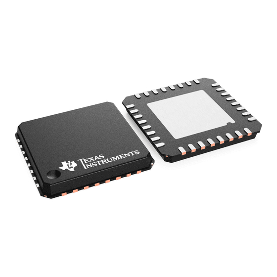
Page 86: Package Description (Qfn 32)
CC1020 Package Description (QFN 32) SWRS046B Page 86 of 91... -
Page 87: Package Marking
CC1020 Quad Flat Pack - No Lead Package (QFN) QFN 32 0.25 0.45 4.18 4.18 0.203 0.65 0.30 0.55 4.28 4.28 45° 0.35 0.65 4.38 4.38 All dimensions in mm. Angles are in degrees. Package is compliant with JEDEC: MO-220. -
Page 88: Recommended Pcb Footprint For Package (Qfn 32)
CC1020 27.2. Recommended PCB Footprint for Package (QFN 32) Note: The figure is an illustration only and not to scale. There are nine 10 mil (0.254 mm) diameter via holes distributed symmetrically in the ground plane under the package. See also the CC1020EMX reference design. -
Page 89: Plastic Tube Specification
CC1020_1070DK-433 CC1020/1070 Development Kit, 433 MHz CC1020_1070DK-868/915 CC1020/1070 Development Kit, 868/915 MHz CC1020SK RoHS CC1020 Sample Kit, QFN32 package, RoHS compliant Pb- free assembly, 5 pcs MOQ = Minimum Order Quantity T&R = tape and reel SWRS046B Page 89 of 91... -
Page 90: General Information
Recommended CAL_ITERATE changed from 5 to 4 PLL timeout in “Automatic power-up sequencing flow chart” changed from 1024 filter clocks to 127 filter clocks Calibration routine flow chart changed in accordance to CC1020 Errata Note Added chapter on TX data latency January 2006... - Page 91 CC1020 Product Status Definitions Data Sheet Identification Product Status Definition Advance Information Planned or Under This data sheet contains the design specifications for Development product development. Specifications may change in any manner without notice. Preliminary Engineering Samples This data sheet contains preliminary data, and and First Production supplementary data will be published at a later date.
- Page 92 PACKAGE MATERIALS INFORMATION www.ti.com 25-Nov-2021 TAPE AND REEL INFORMATION *All dimensions are nominal Device Package Package Pins Reel Reel Pin1 Type Drawing Diameter Width (mm) (mm) (mm) (mm) (mm) Quadrant (mm) W1 (mm) CC1020RSSR 2500 330.0 16.4 12.0 16.0 Pack Materials-Page 1...
- Page 93 PACKAGE MATERIALS INFORMATION www.ti.com 25-Nov-2021 *All dimensions are nominal Device Package Type Package Drawing Pins Length (mm) Width (mm) Height (mm) CC1020RSSR 2500 350.0 350.0 43.0 Pack Materials-Page 2...
- Page 94 TI products. TI’s provision of these resources does not expand or otherwise alter TI’s applicable warranties or warranty disclaimers for TI products. TI objects to and rejects any additional or different terms you may have proposed. IMPORTANT NOTICE Mailing Address: Texas Instruments, Post Office Box 655303, Dallas, Texas 75265 Copyright © 2021, Texas Instruments Incorporated...
Need help?
Do you have a question about the CC1020 and is the answer not in the manual?
Questions and answers