Table of Contents
Advertisement
Quick Links
2.4 GHz IEEE 802.15.4 / ZigBee-ready RF Transceiver
Applications
•
2.4 GHz IEEE 802.15.4 systems
•
ZigBee systems
•
Home/building automation
•
Industrial Control
Product Description
CC2420
The
is a true single-chip 2.4 GHz
IEEE 802.15.4 compliant RF transceiver
designed for low power and low voltage
wireless applications.
digital direct sequence spread spectrum
baseband modem providing a spreading
gain of 9 dB and an effective data rate of
250 kbps.
CC2420
The
is a low-cost, highly integrated
solution for robust wireless communication
in the 2.4 GHz unlicensed ISM band. It
complies
with
worldwide
covered by ETSI EN 300 328 and EN 300
440 class 2 (Europe), FCC CFR47 Part 15
(US) and ARIB STD-T66 (Japan).
CC2420
The
provides extensive hardware
support
for
packet
buffering,
burst
transmissions,
encryption,
data
authentication,
channel assessment, link quality indication
and packet timing information. These
Key Features
•
True
single-chip
802.15.4 compliant RF transceiver
with baseband modem and MAC
support
•
DSSS
baseband
MChips/s and 250 kbps effective data
rate.
•
Suitable for both RFD and FFD
operation
•
Low current consumption (RX: 18.8
mA, TX: 17.4 mA)
•
Low supply voltage (2.1 – 3.6 V) with
integrated voltage regulator
•
Low supply voltage (1.6 – 2.0 V) with
external voltage regulator
CC2420
includes a
regulations
handling,
data
data
clear
2.4
GHz
IEEE
modem
with
2
SWRS041B
•
Wireless sensor networks
•
PC peripherals
•
Consumer Electronics
features reduce the load on the host
CC2420
controller and allow
low-cost microcontrollers.
The configuration interface and transmit /
CC2420
receive FIFOs of
an SPI interface. In a typical application
CC2420
will be used together with a
microcontroller and a few external passive
components.
CC2420
is based on Chipcon's SmartRF
03 technology in 0.18 µm CMOS.
•
Programmable output power
•
No external RF switch / filter needed
•
I/Q low-IF receiver
•
I/Q direct upconversion transmitter
•
Very few external components
•
128(RX) + 128(TX) byte data buffering
•
Digital RSSI / LQI support
•
Hardware MAC encryption (AES-128)
•
Battery monitor
•
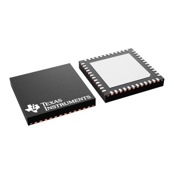
QLP-48 package, 7x7 mm
•
Complies with ETSI EN 300 328, EN
300 440 class 2, FCC CFR-47 part 15
and ARIB STD-T66
•
Powerful and flexible development
tools available
CC2420
to interface
are accessed via
®
-
Page 1 of 89
Advertisement
Table of Contents

Related Manuals for Texas Instruments Chipcon Products CC2420


Summary of Contents for Texas Instruments Chipcon Products CC2420
- Page 1 CC2420 2.4 GHz IEEE 802.15.4 / ZigBee-ready RF Transceiver Applications • • 2.4 GHz IEEE 802.15.4 systems Wireless sensor networks • • ZigBee systems PC peripherals • • Home/building automation Consumer Electronics • Industrial Control Product Description CC2420 features reduce the load on the host is a true single-chip 2.4 GHz CC2420 IEEE 802.15.4 compliant RF transceiver...
-
Page 2: Table Of Contents
CC2420 Table of contents Abbreviations_________________________________________________________________5 References ___________________________________________________________________6 Features _____________________________________________________________________7 Absolute Maximum Ratings _____________________________________________________8 Operating Conditions __________________________________________________________8 Electrical Specifications ________________________________________________________9 Overall ___________________________________________________________________9 Transmit Section ___________________________________________________________9 Receive Section ___________________________________________________________10 RSSI / Carrier Sense _______________________________________________________11 IF Section _______________________________________________________________11 Frequency Synthesizer Section _______________________________________________11 Digital Inputs/Outputs ______________________________________________________12 Voltage Regulator _________________________________________________________13 Battery Monitor ___________________________________________________________13 6.10... - Page 3 CC2420 RF Data Buffering __________________________________________________________39 17.1 Buffered transmit mode _____________________________________________________39 17.2 Buffered receive mode _____________________________________________________39 17.3 Unbuffered, serial mode ____________________________________________________40 Address Recognition ________________________________________________________41 Acknowledge Frames _______________________________________________________41 Radio control state machine __________________________________________________43 MAC Security Operations (Encryption and Authentication) _______________________45 21.1 Keys____________________________________________________________________45 21.2 Nonce / counter ___________________________________________________________45 21.3...
- Page 4 CC2420 40.1 Package thermal properties __________________________________________________84 40.2 Soldering information ______________________________________________________84 40.3 Plastic tube specification ____________________________________________________85 40.4 Carrier tape and reel specification _____________________________________________85 Ordering Information _______________________________________________________85 General Information ________________________________________________________86 42.1 Document History _________________________________________________________86 42.2 Product Status Definitions___________________________________________________87 Address Information ________________________________________________________88 TI Worldwide Technical Support _____________________________________________88 SWRS041B Page 4 of 89...
-
Page 5: Abbreviations
CC2420 Abbreviations Analog to Digital Converter Advanced Encryption Standard Automatic Gain Control ARIB Association of Radio Industries and Businesses Bit Error Rate CBC-MAC Cipher Block Chaining Message Authentication Code Clear Channel Assessment Counter mode + CBC-MAC Code of Federal Regulations CSMA-CA Carrier Sense Multiple Access with Collision Avoidance Counter mode (encryption) -
Page 6: References
CC2420 Synchronisation Header Serial Peripheral Interface To Be Decided / To Be Defined Transmit / Receive Transmit Voltage Controlled Oscillator Variable Gain Amplifier References IEEE std. 802.15.4 - 2003: Wireless Medium Access Control (MAC) and Physical Layer (PHY) specifications for Low Rate Wireless Personal Area Networks (LR-WPANs) http://standards.ieee.org/getieee802/download/802.15.4-2003.pdf NIST FIPS Pub 197: Advanced Encryption Standard (AES), Federal... -
Page 7: Features
CC2420 Features • • 2400 – 2483.5 MHz RF Transceiver 802.15.4 MAC hardware support: • • Direct Sequence Spread Automatic preamble generator • Spectrum (DSSS) transceiver Synchronisation word • 250 kbps data rate, 2 MChip/s insertion/detection chip rate • CRC-16 computation •... -
Page 8: Absolute Maximum Ratings
CC2420 Absolute Maximum Ratings Parameter Min. Max. Units Condition Supply voltage for on-chip voltage regulator, -0.3 VREG_IN pin 43. Supply voltage (VDDIO) for digital I/Os, DVDD3.3, -0.3 pin 25. Supply voltage (VDD) on AVDD_VCO, DVDD1.8, −0.3 etc (pin no 1, 2, 3, 4, 10, 14, 15, 17, 18, 20, 26, 35, 37, 44 and 48) Voltage on any digital I/O pin, (pin no. -
Page 9: Electrical Specifications
CC2420 Electrical Specifications Measured on CC2420 EM with transmission line balun, T = 25 °C, = 3.3 V, internal DVDD3.3 VREG_IN voltage regulator used if nothing else stated. Overall Parameter Min. Typ. Max. Unit Condition / Note RF Frequency Range 2400 2483.5 Programmable in 1 MHz steps, 5... -
Page 10: Receive Section
CC2420 Receive Section Parameter Min. Typ. Max. Unit Condition / Note Receiver Sensitivity PER = 1%, as specified by [1] Measured in a 50Ω single-ended load through a balun. [1] requires –85 dBm Saturation (maximum input level) PER = 1%, as specified by [1] Measured in a 50Ω... -
Page 11: Rssi / Carrier Sense
CC2420 Parameter Min. Typ. Max. Unit Condition / Note Frequency error tolerance -300 Difference between centre frequency of the received RF signal and local oscillator frequency [1] requires 200 kHz Symbol rate error tolerance Difference between incoming symbol rate and the internally generated symbol rate [1] requires 80 ppm Data latency... -
Page 12: Digital Inputs/Outputs
CC2420 Parameter Min. Typ. Max. Unit Condition / Note Crystal load capacitance 16 pF recommended Crystal ESR Ω Crystal oscillator start-up time 16 pF load Phase noise Unmodulated carrier −109 dBc/Hz At ±1 MHz offset from carrier −117 dBc/Hz At ±2 MHz offset from carrier −117 dBc/Hz At ±3 MHz offset from carrier... -
Page 13: Voltage Regulator
CC2420 Voltage Regulator Parameter Min. Typ. Max. Unit Condition / Note General Note that the internal voltage regulator only supply CC2420 and no external circuitry. Input Voltage On the VREG_IN pin Output Voltage On the VREG_OUT pin µA Quiescent current No current drawn from the VREG_OUT pin. - Page 14 CC2420 Parameter Min. Typ. Max. Unit Condition / Note Current Consumption, transmit mode: P = -25 dBm The output power is delivered P = -15 dBm differentially to a 50 Ω singled P = -10 dBm ended load through a balun, see P = −5 dBm also page 54.
-
Page 15: Pin Assignment
CC2420 Pin Assignment VCO_GUARD AVDD_VCO DVDD_RAM AVDD_PRE AVDD_RF1 SCLK CC2420 QLP48 RF_P FIFO TXRX_SWITCH RF_N FIFOP AVDD_SW DVDD1.8 DVDD3.3 AGND Exposed die attach pad CC2420 Figure 1. Pinout – Top View Pin Name Pin type Pin Description Ground (analog) Exposed die attach pad. Must be connected to solid ground AGND plane Power (analog) - Page 16 CC2420 Pin Name Pin type Pin Description Not Connected Power (analog) 1.8 V Power supply for analog parts of ADCs and DACs AVDD_ADC Power (digital) 1.8 V Power supply for digital parts of receive ADCs DVDD_ADC Ground (digital) Ground connection for digital noise isolation DGND_GUARD Power (digital) 1.8 V Power supply connection for digital noise isolation...
-
Page 17: Circuit Description
CC2420 Circuit Description AUTOMATIC GAIN CONTROL DIGITAL DEMODULATOR - Digital RSSI Serial - Gain Control voltage - Image Suppression regulator - Channel Filtering - Demodulation - Frame synchronization TX/RX CONTROL ® SmartRF DIGITAL INTERFACE FREQ CC2420 WITH FIFO SYNTH BUFFERS, CRC AND ENCRYPTION TX POWER CONTROL... - Page 18 CC2420 and Q LO signals to the down-conversion The 4-wire SPI serial interface is used for mixers in receive mode and up-conversion configuration and data buffering. mixers in transmit mode. The VCO operates in the frequency range 4800 – An on-chip voltage regulator delivers the 4966 MHz, and the frequency is divided by regulated 1.8 V supply voltage.
-
Page 19: Application Circuit
CC2420 Application Circuit Few external components are required for If a balanced antenna such as a folded CC2420 dipole is used, the balun can be omitted. If operation typical the antenna also provides a DC path from application circuit is shown in Figure 4. the TXRX_SWITCH pin to the RF pins, The external components shown are described in Table 1 and typical values... - Page 20 CC2420 Description Voltage regulator load capacitance Balun and match DC block to antenna and match Front-end bias decoupling and match Balun and match C381 16MHz crystal load capacitor, see page 53 C391 16MHz crystal load capacitor, see page 53 DC bias and match DC bias and match DC bias and match Balun and match...
- Page 21 CC2420 3.3 V Power supply C391 C381 R451 XTAL VCO_GUARD AVDD_VCO DVDD_RAM Antenna AVDD_PRE (50 Ohm) AVDD_RF1 CC2420 SCLK QLP48 RF_P FIFO TXRX_SWITCH Transceiver FIFOP RF_N AVDD_SW DVDD1.8 DVDD3.3 Figure 4. Typical application circuit with discrete balun for single-ended operation SWRS041B Page 21 of 89...
- Page 22 CC2420 3.3 V Power supply C391 C381 R451 XTAL VCO_GUARD AVDD_VCO DVDD_RAM AVDD_PRE AVDD_RF1 CC2420 SCLK QLP48 RF_P Folded dipole FIFO TXRX_SWITCH Transceiver antenna RF_N FIFOP AVDD_SW DVDD1.8 DVDD3.3 Figure 5. Suggested application circuit with differential antenna (folded dipole) SWRS041B Page 22 of 89...
- Page 23 CC2420 Item Single ended output, Single ended output, Differential antenna transmission line balun discrete balun 10 µF, 0.5Ω < ESR < 5Ω 10 µF, 0.5Ω < ESR < 5Ω 10 µF, 0.5Ω < ESR < 5Ω Not used 0.5 pF, +/- 0.25pF, NP0, 0402 Not used Not used 5.6 pF, +/- 0.25pF, NP0, 0402...
-
Page 24: Ieee 802.15.4 Modulation Format
CC2420 10 IEEE 802.15.4 Modulation Format This section is meant as an introduction to least significant byte is transmitted first, the 2.4 GHz direct sequence spread except for security related fields where the spectrum (DSSS) RF modulation format most significant byte it transmitted first. defined in IEEE 802.15.4. -
Page 25: Configuration Overview
CC2420 I-phase Q-phase Figure 7. I / Q Phases when transmitting a zero-symbol chip sequence, T = 0.5 µs 11 Configuration Overview CC2420 • can be configured to achieve the Power-down / power-up mode best performance different • Crystal oscillator power-up / power applications. -
Page 26: Evaluation Software
CC2420 12 Evaluation Software Texas Instruments (TI) provides users of Studio can be downloaded from TI’s web CC2420 page: http://www.ti.com. Figure 8 shows with software program, ® CC2420 SmartRF Studio (Windows interface) user interface which may be used for radio performance configuration software. -
Page 27: 13 4-Wire Serial Configuration And Data Interface
CC2420 13 4-wire Serial Configuration and Data Interface CC2420 RAM/Register bit (set to 0 for register is configured via a simple 4-wire access), followed by the R/W bit (0 for SPI-compatible interface (pins SI, SO, write, 1 for read). The following 6 bits are CC2420 SCLK and CSn) where is the slave. -
Page 28: Status Byte
CC2420 SCLK Write to register / RXFIFO: 15 D 14 D 13 D 12 D 11 D 10 D Write to TXFIFO: Read from register / RXFIFO: 14 D 13 D 12 D 11 D Read and write one byte to RAM: (multiple read / writes also possible) Read one byte from RAM: (multiple reads also possible) Figure 9. -
Page 29: Command Strobes
CC2420 Bit # Name Description Reserved, ignore value Indicates whether the 16 MHz oscillator is running or not XOSC16M_STABLE 0 : The 16 MHz crystal oscillator is not running 1 : The 16 MHz crystal oscillator is running Indicates whether an FIFO underflow has occurred during TX_UNDERFLOW transmission. - Page 30 CC2420 divided into three memory banks: TXFIFO For RAM read, the selected byte(s) are (bank 0), RXFIFO (bank 1) and security output on the SO pin directly after the (bank 2). The FIFO banks are 128 bytes second address byte. each, while the security bank is 112 bytes.
-
Page 31: Fifo Access
CC2420 Address Byte Ordering Name Description 0x16F – Not used 0x16C 0x16B – 16-bit Short address, used for address recognition. SHORTADR 0x16A 0x169 – 16-bit PAN identifier, used for address recognition. PANID 0x168 0x167 – 64-bit IEEE address of current node, used for address IEEEADR 0x160 recognition. -
Page 32: Microcontroller Interface And Pin Description
CC2420 ADDR ADDR ADDR DATA DATA DATA TXFIFO ADDR ADDR+1 ADDR+2 Status Status DATA DATA Status Status Status Status 8MSB 8LSB Command Register TXFIFO Strobe Read Write Figure 11. Multiple SPI Access Example 14 Microcontroller Interface and Pin Description CC2420 configuration interface (SI, SO, SCLK and When used in a typical system, will... -
Page 33: Receive Mode
CC2420 recognition. This may be handled by using 14.2 Receive mode the FIFOP pin, since this pin does not go In receive mode, the SFD pin goes active active until the frame passes address recognition. after the start of frame delimiter (SFD) field has been completely received. -
Page 34: Transmit Mode
CC2420 Data received over RF Preamble SFD Length MAC Protocol Data Unit (MPDU) with correct address Address SFD Pin recognition OK FIFO Pin FIFOP Pin, if threshold higher than frame length FIFOP Pin, if threshold lower than frame length Data received over RF Preamble SFD Length MAC Protocol Data Unit (MPDU) with wrong address... -
Page 35: General Control And Status Pins
CC2420 Data transmitted Preamble SFD Length MAC Protocol Data Unit (MPDU) over RF SFD Pin CRC generated 12 symbol periods Automatically generated Data fetched CC2420 preamble and SFD from TXFIFO Figure 15. Pin activity example during transmit received data frames. The SFD pin will go 14.5 General control and status pins active when a start of frame delimiter has In receive mode, the FIFOP pin can be... -
Page 36: Frame Format
CC2420 Digital Frequency Digital Symbol Data I / Q Analog IF Channel Offset Data Correlators and Symbol IF signal Filtering Compensation Filtering Synchronisation Output Average RSSI Correlation RSSI Value (may be Generator used for LQI) Figure 16. Demodulator Simplified Block Diagram 16 Frame Format CC2420 Figure 17 [1] shows a schematic view of... -
Page 37: Length Field
CC2420 additional zero symbols in SYNCWORD right) 0 7 A. If SYNCWORD = 0xA70F, CC2420 CC2420 make compliant with [1]. will require the incoming symbol sequence of (from left to right) 0 0 7 A. If CC2420 CC2420 SYNCWORD = 0xA700, will require In reception, synchronises to... -
Page 38: Frame Check Sequence
CC2420 CC2420 There is no hardware support for the data includes hardware address sequence number, this field must be recognition, as described in the Address inserted and verified by software. Recognition section on page 41. Bits: 0-2 10-11 12-13 14-15 Frame Security Frame... -
Page 39: Rf Data Buffering
CC2420 Length byte MPDU RSSI Data in RXFIFO MPDU MPDU MPDU CRC / Corr (signed) Bit number Correlation value (unsigned) Figure 21. Data in RXFIFO when MDMCTRL0.AUTOCRC is set 17 RF Data Buffering CC2420 A TXFIFO underflow is issued if too few can be configured for different bytes written... -
Page 40: Unbuffered, Serial Mode
CC2420 Multiple data frames may be in the serial transmit mode RXFIFO simultaneously, as long as the (MDMCTRL1.TX_MODE=1), total number of bytes does not exceed synchronisation sequence is inserted at 128. the start of each frame by hardware, as in CC2420 buffered mode. -
Page 41: Address Recognition
CC2420 18 Address Recognition CC2420 identifier matches includes hardware support for macPANId. address recognition, as specified in [1]. Hardware address recognition may be enabled disabled using If any of the above requirements are not MDMCTRL0.ADR_DECODE control bit. satisfied address recognition CC2420 enabled, will... - Page 42 CC2420 AUTOACK may be used for non-beacon symbol periods after the last symbol of the incoming frame. This is as specified by [1] systems as long as the frame pending for non-beacon networks. field (see Figure 19) is cleared. The acknowledge frame is then transmitted 12 Bytes: Start of Frame...
-
Page 43: Radio Control State Machine
CC2420 20 Radio control state machine CC2420 test purposes, frequency has a built-in state machine that is synthesizer (FS) can also be manually used switch between different calibrated and started by using the operational states (modes). The change of STXCAL command strobe register. This state is done either by using command strobes or by internal events such as SFD will not start a transmission before a... - Page 44 CC2420 Voltage Regulator Off VREG_EN set low VREG_EN set high Wait until voltage regulator has powered up Chip Reset (pin or register) SXOSCOFF Crystal oscillator disabled, command strobe Power Down (PD) All States register access enabled, FIFO / RAM access disabled SXOSCON Wait for the specified crystal oscillator start-up time, or poll the...
-
Page 45: Mac Security Operations (Encryption And Authentication)
CC2420 21 MAC Security Operations (Encryption and Authentication) CC2420 As can be seen from Table 6 on page 31, features hardware IEEE 802.15.4 KEY0 is located from address 0x100 and MAC security operations. This includes KEY1 from address 0x130. counter mode (CTR) encryption... -
Page 46: Stand-Alone Encryption
CC2420 flag setting is stored in the most significant The frame counter part of the nonce must byte of the nonce. The flag byte used for be incremented for each new packet by encryption and authentication is then software. generated as shown in Figure 26. MSB in CC2420 nonce RAM CTR Flag CBC Flag... -
Page 47: Ctr Mode Encryption / Decryption
CC2420 RX in-line security operations are always of the RXFIFO is then decrypted as performed on the first frame currently specified by [1]. inside the RXFIFO, even if parts of this have already been read out over the SPI 21.6 CBC-MAC interface. -
Page 48: Timing
CC2420 Table 8 shows some examples of the time 21.8 Timing used by the security module for different operations. Mode l(a) l(m) l(MIC) Time [us] Stand- alone Table 8. Security timing examples 22 Linear IF and AGC Settings CC2420 dynamic range by using an analog/digital is based on a linear IF chain feedback loop. -
Page 49: Link Quality Indication
CC2420 -100 RF Level [dBm] Figure 27. Typical RSSI value vs. input power 24 Link Quality Indication link quality indication (LQI) described Frame check measurement is a characterisation of the sequence section on page 38, the average strength and/or quality of a received correlation value for the 8 first symbols is packet, as defined by [1]. -
Page 50: Clear Channel Assessment
CC2420 25 Clear Channel Assessment The clear channel assessment signal is Reserved based on the measured RSSI value and a Clear channel when received energy is below programmable threshold. clear threshold. channel assessment function is used to Clear channel when not receiving valid IEEE implement the CSMA-CA functionality 802.15.4 data. -
Page 51: Vco And Pll Self-Calibration
CC2420 27 VCO and PLL Self-Calibration In order to ensure reliable operation the 27.1 VCO VCO’s bias current and tuning range are automatically calibrated every time the RX The VCO is completely integrated and mode or TX mode is enabled, i.e. in the operates at 4800 –... -
Page 52: Battery Monitor
CC2420 In applications where the internal voltage be left open. Note that the battery monitor regulator is not used, connect VREG_EN will not work when the voltage regulator is not used. and VREG_IN to ground. VREG_OUT shall VREG_EN VREG_IN Regulator Enable / disable Internal bandgap... -
Page 53: Crystal Oscillator
CC2420 The battery monitor is controlled through Alternatively, for a desired toggle voltage, the BATTMON control register. The battery should BATTMON_VOLTAGE monitor is enabled and disabled using the according to: BATTMON.BATTMON_EN control bit. The voltage regulator must also be enabled −... -
Page 54: Input / Output Matching
CC2420 XOSC16_Q1 XOSC16_Q1 XOSC16_Q2 XOSC16_Q2 XTAL XTAL XTAL C391 C391 C381 C381 Figure 30. Crystal oscillator circuit Item = 16 pF C381 27 pF C391 27 pF Table 10. Crystal oscillator component values 32 Input / Output Matching The RF input / output is differential (RF_N Component values are given in Table 2. -
Page 55: Modulated Spectrum
CC2420 10 kHz RF Att 30 dB Ref Lvl Ref Lvl 10 kHz 3 dBm 3 dBm 50 ms Unit 1AVG Center 2.45 GHz 200 kHz/ Span 2 MHz Date: 23.OCT.2003 21:38:33 Figure 31. Single carrier output sequence for bit error testing. Please note 33.2 Modulated spectrum CC2420 that... - Page 56 CC2420 100 kHz RF Att 30 dB Ref Lvl Ref Lvl 100 kHz 0 dBm 0 dBm 5 ms Unit 1AVG -100 Center 2.45 GHz 1 MHz/ Span 10 MHz Date: 23.OCT.2003 21:34:19 Figure 32. Modulated spectrum plot SWRS041B Page 56 of 89...
-
Page 57: System Considerations And Guidelines
CC2420 34 System Considerations and Guidelines SRD regulations 34.3 Crystal accuracy and drift International regulations and national laws A crystal accuracy of ±40 ppm is required regulate the use of radio receivers and for compliance with IEEE 802.15.4 [1]. transmitters. SRDs (Short Range Devices) This accuracy must also take ageing and for license free operation are allowed to temperature drift into consideration. -
Page 58: Low-Cost Systems
CC2420 required re-gain 34.6 Low-cost systems synchronisation. CC2420 As the provides 250 kbps multi- channel performance without any external IEEE 802.15.4 system, filters, a very low-cost system can be communication is based on packets. The made. sensitivity limit specified by [1] is based on Packet Error Rate (PER) measurements A differential antenna will eliminate the instead of BER. -
Page 59: Pcb Layout Recommendations
The de- files for the reference designs are all coupling capacitors should also be placed available from the Texas Instruments as close as possible to the supply pins website. and connected to the ground plane by... - Page 60 CC2420 of the antenna. Many vendors offer such (λ/4). They are very easy to design and antennas intended for PCB mounting. can be implemented simply as a “piece of wire” or even integrated into the PCB. Helical antennas can be thought of as a combination of a monopole and a loop antenna.
-
Page 61: Configuration Registers
CC2420 37 Configuration Registers CC2420 are 33 normal 16-bits registers, also listed The configuration of is done by in Table 11. Many of these registers are programming 16-bit configuration for test purposes only, and need not be registers. Complete descriptions of the CC2420 registers are given in the following tables. - Page 62 CC2420 Address Register Register type Description 0x0E AES Stand alone encryption strobe. SPI_SEC_MODE is not SAES required to be 0, but the encryption module must be idle. If not, the strobe is ignored. 0x0F Not used 0x10 Main Control Register MAIN 0x11 Modem Control Register 0...
- Page 63 CC2420 MAIN (0x10) - Main Control Register Field Name Reset Description Active low reset of the entire circuit should be applied before RESETn doing anything else. Equivalent to using the RESETn reset pin. Active low reset of the encryption module. (Test purposes only) ENC_RESETn Active low reset of the demodulator module.
- Page 64 CC2420 MDMCTRL0 (0x11) - Modem Control Register 0 Field Name Reset Description Reserved, write as 0 15:14 Mode for accepting reserved IEE 802.15.4 frame types when RESERVED_FRAME_MODE address recognition is enabled ( MDMCTRL0.ADR_DECODE = 1 0 : Reserved frame types (100, 101, 110, 111) are rejected by address recognition.
- Page 65 CC2420 MDMCTRL1 (0x12)– Modem Control Register 1 Field Name Reset Description Reserved, write as 0. 15:11 Demodulator correlator threshold value, required before SFD 10:6 CORR_THR[4:0] search. Note that on early CC2420 versions the reset value was Frequency offset average filter behaviour. DEMOD_AVG_MODE 0 : Lock frequency offset filter after preamble match 1 : Continuously update frequency offset filter.
- Page 66 CC2420 SYNCWORD (0x14) - Sync Word Field Name Reset Description Synchronisation word. The SYNCWORD is processed from the 15:0 SYNCWORD[15:0] 0xA70F least significant nibble (F at reset) to the most significant nibble (A at reset). SYNCWORD is used both during modulation (where 0xF’s are replaced with 0x0’s) and during demodulation (where 0xF’s are not required for frame synchronisation).
- Page 67 CC2420 RXCTRL0 (0x16) – Receive control register 0 Field Name Reset Description Reserved, write as 0. 15:14 RX mixer buffer bias current. 13:12 RXMIXBUF_CUR[1:0] 0: 690uA 1: 980uA (nominal) 2: 1.16mA 3: 1.44mA Controls current in the LNA gain compensation branch in AGC 11:10 HIGH_LNA_GAIN[1:0] High gain mode.
- Page 68 CC2420 RXCTRL1 (0x17) - Receive control register 1 Field Name Reset Description Reserved, write as 0. 15:14 Controls reference bias current to RX bandpass filters: RXBPF_LOCUR 0: 4 uA (Reset value) Use 1 instead 1: 3 uA Note: Recommended setting Controls reference bias current to RX bandpass filters: RXBPF_MIDCUR 0: 4 uA (Default)
- Page 69 CC2420 FSCTRL (0x18) - Frequency Synthesizer Control and Status Field Name Reset Description Number of consecutive reference clock periods with successful 15:14 LOCK_THR[1:0] synchronisation windows required to indicate lock: 0: 64 1: 128 (recommended) 2: 256 3: 512 Calibration has been performed since the last time the frequency CAL_DONE synthesizer was turned on.
- Page 70 CC2420 SECCTRL0 (0x19) - Security Control Register Field Name Reset Description Reserved, write as 0 15:10 Protection enable of the RXFIFO, see description in the RXFIFO RXFIFO_PROTECTION overflow section on page 33. Should be cleared if MAC level security is not used or is implemented outside CC2420. Defines what to use for the first byte in CBC-MAC (does not SEC_CBC_HEAD apply to CBC-MAC part of CCM):...
- Page 71 CC2420 SECCTRL1 (0x1A) - Security Control Register Field Name Reset Description Reserved, write as 0 Multi-purpose length byte for TX in-line security operations: 14:8 SEC_TXL CTR : Number of cleartext bytes between length byte and the first byte to be encrypted CBC/MAC : Number of cleartext bytes between length byte and the first byte to be authenticated CCM : l(a), defining the number of bytes to be authenticated but...
- Page 72 CC2420 IOCFG0 (0x1C) – I/O Configuration Register 0 Field Name Reset Description Reserved, write as 0 15:12 Accept all beacon frames when address recognition is enabled. BCN_ACCEPT This bit should be set when the PAN identifier programmed into CC2420 RAM is equal to 0xFFFF and cleared otherwise. This bit is don't care when MDMCTRL0.ADR_DECODE = 0.
- Page 73 CC2420 MANFIDH (0x1F) - Manufacturer ID, Upper 16 Bit Field Name Reset Description Version number. Current version is 3. 15:12 VERSION[3:0] Note that previous CC2420 versions will have lower reset values. The device part number. CC2420 has part number 0x002. 11:0 PARTNUM[15:4] FSMTC (0x20) - Finite state machine time constants...
- Page 74 CC2420 MANAND (0x21) - Manual signal AND override register Field Name Reset Description The VGA_RESET_N signal is used to reset the peak detectors in VGA_RESET_N the VGA in the RX chain. Global bias power down (1) BIAS_PD The BALUN_CTRL signal controls whether the PA should BALUN_CTRL receive its required external biasing (1) or not (0) by controlling the RX/TX output switch.
- Page 75 CC2420 MANOR (0x22) - Manual signal OR override register Field Name Reset Description The VGA_RESET_N signal is used to reset the peak detectors in VGA_RESET_N the VGA in the RX chain. Global Bias power down (1) BIAS_PD The BALUN_CTRL signal controls whether the PA should receive BALUN_CTRL its required external biasing (1) or not (0) by controlling the RX/TX output switch.
- Page 76 CC2420 AGCTST0 (0x24) - AGC Test Register 0 Field Name Reset Description Hysteresis on the switching between different RF front-end 15:12 LNAMIX_HYST[3:0] gain modes, defined in 2 dB steps Threshold for switching between medium and high RF front- 11:6 LNAMIX_THR_H[5:0] end gain mode, defined in 2 dB steps Threshold for switching between low and medium RF front-end LNAMIX_THR_L[5:0]...
- Page 77 CC2420 FSTST0 (0x27) - Frequency Synthesizer Test Register 0 Field Name Reset Description Reserved, write as 0 15:12 When '1' this control bit doubles the time allowed for VCO VCO_ARRAY_SETTLE_LONG settling during VCO calibration. VCO array manual override enable. VCO_ARRAY_OE VCO array override value.
- Page 78 CC2420 FSTST3 (0x2A) - Frequency Synthesizer Test Register 3 Field Name Reset Description Disable charge pump during VCO calibration when set. CHP_CAL_DISABLE Charge pump current override enable CHP_CURRENT_OE 0 : Charge pump current set by calibration 1 : Charge pump current set by START_CHP_CURRENT Forces the CHP to output "up"...
- Page 79 CC2420 ADCTST (0x2D) - ADC Test Register Field Name Reset Description ADC Clock Disable ADC_CLOCK_DISABLE 0 : Clock enabled when ADC enabled 1 : Clock disabled, even if ADC is enabled Read the current ADC I-branch value. 14:8 ADC_I[6:0] Reserved, write as 0. Read the current ADC Q-branch value.
- Page 80 CC2420 TOPTST (0x2F) - Top Level Test Register Field Name Reset Description Reserved, write as 0. 15:8 Enable BIST of the RAM RAM_BIST_RUN 0 : RAM BIST disabled, normal operation 1 : RAM BIST Enabled. Result output to pin, as set in IOCFG1. Enable test output of the battery monitor.
-
Page 81: Test Output Signals
CC2420 38 Test Output Signals The two digital output pins CCA and SFD, IOCFG1.SFDMUX. This is summarized in can be set up to output test signals Table 12 and Table 13 below. defined IOCFG1.CCAMUX CCAMUX Signal output on CCA pin Description Normal operation ADC_Q[0]... - Page 82 CC2420 SFDMUX Signal output on SFD pin Description Normal operation ADC_I[0] ADC, I-branch, LSB used for random number generation DEMOD_RESYNCH_EARLY High one 16 MHz clock cycle each time the demodulator resynchronises early LOCK_STATUS Lock status, same as FSCTRL.LOCK_STATUS MOD_CHIP Chip rate data signal during transmission MOD_SERIAL_DATA_OUT Bit rate data signal during transmission FFCTRL_FS_PD...
-
Page 83: Package Description (Qlp 48)
CC2420 39 Package Description (QLP 48) Note: The figure is an illustration only and not to scale. Quad Leadless Package (QLP) QLP 48 6.65 6.65 0.18 5.05 5.05 6.75 6.75 5.10 5.10 6.85 6.85 0.30 5.15 5.15 The overall packet height is 0.85 +/- 0.05 All dimensions in mm The package is compliant to JEDEC standard MO-220. -
Page 84: Recommended Layout For Package (Qlp 48)
CC2420 40 Recommended layout for package (QLP 48) Note: The figure is an illustration only and not to scale. There are nine 14 mil diameter via holes distributed symmetrically in the ground pad under the package. See also the CC2420 EM reference design. -
Page 85: Plastic Tube Specification
CC2420 40.3 Plastic tube specification QLP 7x7mm antistatic tube. Tube Specification Package Tube Width Tube Height Tube Length Units per Tube QLP 48 8.5 ± 0.2 mm 2.2 +0.2/-0.1 mm 315 ± 1.25 mm 40.4 Carrier tape and reel specification Carrier tape and reel is in accordance with EIA Specification 481. -
Page 86: General Information
CC2420 42 General Information 42.1 Document History Revision Date Description/Changes SWRS041b 2007-03-19 Slightly changed optimum load impedance on Page 9 and 19 to better describe the Application circuit. SWRS041a 2006-12-18 Updated ordering information. Updated address information. Typical data latency changed from 2 to 3 us. Updates reflecting the programmable polarity of FIFO, FIFOP, SFD and CCA pins. -
Page 87: Product Status Definitions
CC2420 Revision Date Description/Changes 2004-06-09 Output power range: 24 dB (was 40 dB). Deleted option for single ended external PA. Adjacent channel rejection corrected to 46 dB for + 5MHz (was 39 dB), 39 dB for –5 MHz (was 46 dB) 58 dB for +10 MHz (was 53 dB) and 55 dB for-10 MHz (was 57 dB). “image channel”... -
Page 88: Address Information
CC2420 43 Address Information Texas Instruments Norway AS Gaustadalléen 21 N-0349 Oslo NORWAY Tel: +47 22 95 85 44 Fax: +47 22 95 85 46 Web site: http://www.ti.com/lpwrf 44 TI Worldwide Technical Support Internet TI Semiconductor Product Information Center Home Page: support.ti.com... - Page 89 800-96-5941 India +91-80-51381665 (Toll) Indonesia 001-803-8861-1006 Korea 080-551-2804 Malaysia 1-800-80-3973 New Zealand 0800-446-934 Philippines 1-800-765-7404 Singapore 800-886-1028 Taiwan 0800-006800 Thailand 001-800-886-0010 +886-2-2378-6808 tiasia@ti.com or ti-china@ti.com Email support.ti.com/sc/pic/asia.htm Internet © 2007, Texas Instruments. All rights reserved. SWRS041B Page 89 of 89...
-
Page 90: Important Notice
TI as compliant with ISO/TS 16949 requirements. Buyers acknowledge and agree that, if they use any non-designated products in automotive applications, TI will not be responsible for any failure to meet such requirements. Following are URLs where you can obtain information on other Texas Instruments products and application solutions: Products...
Need help?
Do you have a question about the Chipcon Products CC2420 and is the answer not in the manual?
Questions and answers