Advertisement
Quick Links
Advertisement

Related Manuals for Texas Instruments TMS3705A


Summary of Contents for Texas Instruments TMS3705A
- Page 1 LF Technical Training TMS3705A Transceiver IC J.A.G Aug 2006...
-
Page 2: Main Features
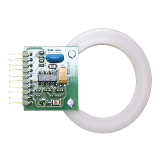
►Main Features 5V device Automatic sleep mode (TXCT idle for 100 ms) Transponder resonance frequency measurement Internal Full Bridge antenna driver 9.35 mm Digital demodulator 6.12 mm Diagnosis function Several operating modes ♦ self adapting or fixed frequency charge-up ♦ automatic or fixed demodulator threshold ♦... - Page 3 ►A Transceiver Module with antenna J.A.G Aug 2006...
- Page 4 ►Pin Names & Functions NAME DESCRIPTION SENSE Input of RF amplifier Output of RF amplifier D Package D_TST Test output for digital signals (Top view) A_TST Test output for analog signals ANT1 Antenna output 1 SENSE TXCT VSSA Ground for full bridge drivers F_SEL ANT2 Antenna output 2...
-
Page 5: Block Diagram
►Block Diagram SCI- Digital Encoder Demodulator Diagnosis Limiter Tag Resonant - A_TST SCIO Freq. Measurement Band Pass Power- on reset Control Logic RFAmplifier with Mode Control TXCT Vref Register SENSE D_TST Full Bridge VDDA F_SEL Controlled ANT1 Pre- Frequency Divider drivers OSC2 ANT2... - Page 6 ►Generic Circuit Diagram TXCT (input) SENSE TXCT F_SEL SCIO (output) D_TST SCIO A_TST VSSB ANT1 ANTENNA VSSA OSC1 ANT2 OSC2 VDDA 4 MHz Supply Voltage Ground J.A.G Aug 2006...
- Page 7 ►Power Supply and Blocking Capacitance To prevent uncontrolled radiation it is recommended to connect the supply voltage symmetrically to VDDA and VDD Connect the blocking capacitors as close as possible to the supply pins VDDA Tantalum capacitors are recommended J.A.G Aug 2006...
- Page 8 ►Oscillator - PLL F_SEL OSC2 OSC1 VSSB If a Ceramic Oscillator is to be used, one with an internal load capacitance of around 56 pF is recommended An external oscillator signal can be fed into OSC1. OSC2 has to be left open - a decoupling capacitor is recommended. J.A.G Aug 2006...
- Page 9 ►The Digital Demodulator SCI- Digital Encoder Demodulator Transponder Resonance - SCIO Frequency Measurement The input frequency is measured by counting the oscillation clock for the time period of the input signal. The demodulator distinguishes between the high-bit frequency and the low-bit frequency by the shift values and by the absolute values.
- Page 10 ►Tag Resonant Frequency Measurement When TXCT goes high, the module enters the read phase Frequency measuring Begins looking for start starts (Pre-bits) byte (0x7E, 0x7F)) TXCT 100 µs 1.6 ms 1.7 ms SCIO Start Bit 1.6 ms after TXCT goes high, an internal measuring cycle of 100 µs will start to measure the low bit frequency of the 16 tag pre-bits.
- Page 11 ►Diagnostics Byte Diagnosis A_TST SENSE The diagnostics byte is sent 2 ms after the start of the charge phase ♦ If normal antenna operation is detected then 0xAF is sent ♦ If no antenna oscillation is detected or a short detection occurs, then 0xFF is sent J.A.G Aug 2006...
- Page 12 ►RX Amplifier Diagnosis Limiter A_TST Band Pass RF Amplifier Vref SENSE The OP Amp has a fixed internal voltage reference A voltage gain of 5 is controlled by external resistance 150k = 3.19 J.A.G Aug 2006...
- Page 13 ►Band-Pass Filter & Limiter Diagnosis Limiter A_TST Band Pass RF Amplifier Vref SENSE No external components required for filtering and amplification The analog sine-wave is converted to a digital signal High gain - at least 1000 J.A.G Aug 2006...
- Page 14 ►SCI Encoder for Data Transmission to the Controller SCI- Digital Encoder Demodulator Transponder Resonance - SCIO Frequency Measurement An 8-bit shift register is used to buffer and send the received data byte-wise to the micro controller (Least Significant Bit first) In Synchronous Mode, a high state at the SCSI output indicates that a new byte is ready to be transmitted The transmission rate is 15625 baud (in asynchronous mode)
- Page 15 ►SCI Encoder for Data Transmission to the Controller (2) SCI- Digital Encoder Demodulator SCIO Transponder Resonance - Frequency Measurement The Start-Byte is the first byte sent to the microcontroller. Data bits at the SCIO output are inverted compared with the data from a transponder.
- Page 16 ►SCIO Asynchronous Transmission Timing diagram Stop Start SCIO J.A.G Aug 2006...
- Page 17 ►SCIO Synchronous Transmission Timing diagram SCIO Byte Stop ready ‘bit’ TxCT L_sync ready sync t_sync µP Reads data Shift data J.A.G Aug 2006...
- Page 18 ►SCIO in Synchronous Transmission Mode The SCI encoder can be switched into synchronous transmission mode by setting the SCI_Sync bit in the Mode Control Register (MCR) The micro-controller has to clock out the data bytes by sending 8 clock signals to the TXCT input A high state on the SCIO indicates that a new byte is ready to be transmitted.
-
Page 19: Mode Control Register
►Mode Control Register (MCR) By writing to the MCR the SCI- mode of operation of the IC Digital Encoder Demodulator can be changed. Transponder Resonance - SCIO Frequency Measurement The options include: ♦ Asynchronous/ Synchronous Power-on Reset data Control Logic with TXCT ♦... - Page 20 ►Timing Diagram Mode Control Register Write Protocol TxCT init PHASE Low Bit 1 Bit 2 Bit 3 Bit 4 Bit 5 Bit 6 Bit 7 CHARGE Start bit Test bit Init. Transmission End of transmission J.A.G Aug 2006...
- Page 21 ►7-bit Mode Control Register (MCR) Bit 0 Start Bit Start bit is always LOW Bit 1 Frequency selection/ Threshold adjust Bit 2 Frequency selection/ Threshold adjust Bit 3 Frequency selection/ Threshold adjust Bit 4 Frequency selection/ Threshold adjust Bit 5 SCI_Sync 0 (default) Asynchronous data transmission...
-
Page 22: Frequency Selection
►Frequency Selection (MCR) Bit 0 Bit 1 Bit 2 Bit 3 Bit 4 Division Notes Factor Division factor selected by µC - Default Division factor selected by µC Division factor selected by µC Division factor selected by µC Division factor selected by µC Division factor selected by µC Division factor selected by µC Division factor selected by µC... - Page 23 ►Timing Diagram: Default mode Write to MCR TxCT D = Diagnosis Byte, S = Start Byte SCIO Data Bytes init diags PHASE M.C.W. CHARGE RESPONSE Init. Transmission J.A.G Aug 2006...
- Page 24 ►Timing Diagram: R/O mode With write to MCR TxCT D = Diagnosis Byte, S = Start Byte SCIO Data Bytes wake init ~50µs diags PHASE M.C.W. CHARGE RESPONSE Init. Transmission NOTE: For correct writing to the MCR, it is essential to know if the IC is in IDLE or SLEEP mode J.A.G Aug 2006...
- Page 25 ►Timing Diagram: R/W mode With write to MCR TxCT D = Diagnosis Byte, S = Start Byte SCIO Data Bytes prog wake init ~50µs diags PHASE M.C.W. CHARGE WRITE PROG RESPONSE Init. Transmission NOTE: For correct writing to the MCR, it is essential to know if the IC is in IDLE or SLEEP mode J.A.G Aug 2006...
-
Page 26: State Diagram
►State Diagram: POWER ~ 2 ms AFTER TxCT AFTER ~ 2 ms SLEEP GOES LOW TxCT IS LOW AFTER ~ 100 ms IDLE MCR Programming TxCT GOES 0.9 ms after TxCT goes low Write bits into HIGH < 90 MS or ~ 4ms after the start of Receive Mode Control Register phase if no start bit is detected... - Page 27 ►State Notes: Notes: 1. In SCI synchronous mode, this transition always occurs approximately 3 ms after leaving Idle state. The diagnostics byte transmission should have completed. 2. A falling edge on TxCT interrupts the Receive phase after a delay of 0.9 ms. TxCT must remain low for at least 128 IDLE µs.
- Page 28 ►Guidelines TMS3705A Data Sheet [Rev 1.0 - June 1999] Application Note [11-07-26-001. Oct 1999] DST Reference Manual [11-09-21-029. Dec 1998] DST Sequence Control Specification [24-06-05-005. Jun 1996] DSP Algorithm & SW Requirements [24-09-05-012. Oct 1995] Immobiliser Systems Design Guide [Rev .01 Jan 1996] Tricks and Hints for System Evaluation [Ver 2.0 Sept 1999]...
Need help?
Do you have a question about the TMS3705A and is the answer not in the manual?
Questions and answers