Table of Contents
Advertisement
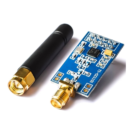
Low-Power Sub-1 GHz RF Transceiver
Applications
Ultra
low-power
operating in the 315/433/868/915 MHz
ISM/SRD bands
Wireless alarm and security systems
Industrial monitoring and control
Product Description
CC1101
is a low-cost sub-1 GHz transceiver
designed for very low-power wireless appli-
cations. The circuit is mainly intended for the
ISM (Industrial, Scientific and Medical) and
SRD (Short Range Device) frequency bands
at 315, 433, 868, and 915 MHz, but can easily
be
programmed
for
frequencies in the 300-348 MHz, 387-464 MHz
and 779-928 MHz bands.
The RF transceiver is integrated with a highly
configurable baseband modem. The modem
supports various modulation formats and has
a configurable data rate up to 600 kbps.
CC1101
provides extensive hardware support
for packet handling, data buffering, burst
transmissions, clear channel assessment, link
quality indication, and wake-on-radio.
The main operating parameters and the 64-
byte transmit/receive FIFOs of
controlled via an SPI interface. In a typical
CC1101
system, the
will be used together with a
wireless
applications
operation
at
other
CC1101
can be
SWRS061H
Wireless sensor networks
AMR – Automatic Meter Reading
Home and building automation
Wireless MBUS
microcontroller and a few additional passive
components.
CC1190
The
850-950 MHz range extender [21]
CC1101
can be used with
applications for improved sensitivity and higher
output power.
1
15
CC1101
2
14
3
13
4
12
5
11
CC1101
in long range
Page 1 of 98
Advertisement
Table of Contents

Related Manuals for Texas Instruments CC1101


Summary of Contents for Texas Instruments CC1101
-
Page 1: Applications
CC1101 Low-Power Sub-1 GHz RF Transceiver Applications Ultra Wireless sensor networks low-power wireless applications AMR – Automatic Meter Reading operating in the 315/433/868/915 MHz Home and building automation ISM/SRD bands Wireless alarm and security systems ... -
Page 2: Key Features
CC1101 Key Features RF Performance Low-Power Features 200 nA sleep mode current consumption High sensitivity Fast startup time; 240 μs from sleep to RX -116 dBm at 0.6 kBaud, 433 MHz, or TX mode (measured on EM reference... -
Page 3: Reduced Battery Current Using Tps62730
3.6 V Figure 1: Typical RX Battery Current vs Battery Voltage Figure 2: Typical TX Battery Current vs Battery Voltage at Maximum CC1101 Output Power (+12 dBm) SWRS061H Page 3 of 98... -
Page 4: Abbreviations
CC1101 Abbreviations Abbreviations used in this data sheet are described below. 2-FSK Binary Frequency Shift Keying Most Significant Bit 4-FSK Quaternary Frequency Shift Keying Minimum Shift Keying Adjacent Channel Power Not Applicable Analog to Digital Converter Non Return to Zero (Coding) -
Page 5: Table Of Contents
CC1101 Table Of Contents APPLICATIONS ..............................1 PRODUCT DESCRIPTION ..........................1 KEY FEATURES ..............................2 RF PERFORMANCE ............................2 ANALOG FEATURES ............................2 DIGITAL FEATURES ............................2 LOW-POWER FEATURES ..........................2 GENERAL ................................2 IMPROVED RANGE USING CC1190 ......................2 REDUCED BATTERY CURRENT USING TPS62730 .................. - Page 6 CC1101 RECEIVER CHANNEL FILTER BANDWIDTH ................35 DEMODULATOR, SYMBOL SYNCHRONIZER, AND DATA DECISION ........36 14.1 ......................36 REQUENCY FFSET OMPENSATION 14.2 ..........................36 YNCHRONIZATION 14.3 .......................... 36 YNCHRONIZATION PACKET HANDLING HARDWARE SUPPORT ................37 15.1 ............................. 37 HITENING 15.2 ............................
- Page 7 CC1101 CONFIGURATION REGISTERS ......................66 – R 29.1 SLEEP ....71 ONFIGURATION EGISTER ETAILS EGISTERS WITH PRESERVED VALUES IN STATE – R 29.2 SLEEP S ..91 ONFIGURATION EGISTER ETAILS EGISTERS THAT OOSE ROGRAMMING IN TATE 29.3 ........................92 TATUS...
-
Page 8: Absolute Maximum Ratings
CC1101 Absolute Maximum Ratings Under no circumstances must the absolute maximum ratings given in Table 1 be violated. Stress exceeding one or more of the limiting values may cause permanent damage to the device. Parameter Units Condition –0.3 Supply voltage All supply pins must have the same voltage –0.3... -
Page 9: Electrical Specifications
CC1101 Electrical Specifications Current Consumption = 25C, VDD = 3.0 V if nothing else stated. All measurement results are obtained using the CC1101EM reference designs ([1] and [2]). Reduced current settings (MDMCFG2.DEM_DCFILT_OFF=1) gives a slightly lower current consumption at the cost of a reduction in sensitivity. - Page 10 CC1101 Parameter Unit Condition Current consumption, 16.0 Receive mode, 1.2 kBaud, register settings optimized for reduced 433 MHz current, input at sensitivity limit 15.0 Receive mode, 1.2 kBaud, register settings optimized for reduced current, input well above sensitivity limit 15.7 Receive mode, 38.4 kBaud, register settings optimized for...
- Page 11 CC1101 Supply Voltage Supply Voltage Supply Voltage VDD = 1.8 V VDD = 3.0 V VDD = 3.6 V Temperature [°C] Current [mA], PATABLE=0xC0, 32.7 31.5 30.5 35.3 34.2 33.3 35.5 34.4 33.5 +12 dBm Current [mA], PATABLE=0xC5, 30.1 29.2 28.3...
-
Page 12: Rf Receive Section
CC1101 RF Receive Section = 25C, VDD = 3.0 V if nothing else stated. All measurement results are obtained using the CC1101EM reference designs ([1] and [2]). Parameter Unit Condition/Note Digital channel filter User programmable. The bandwidth limits are proportional to bandwidth crystal frequency (given values assume a 26.0 MHz crystal) - Page 13 CC1101 Parameter Unit Condition/Note Blocking Desired channel 3 dB above the sensitivity limit ±2 MHz offset See Figure 4 for blocking performance at other offset ±10 MHz offset frequencies 38.4 kBaud data rate, sensitivity optimized, MDMCFG2.DEM_DCFILT_OFF=0 (GFSK, 1% packet error rate, 20 bytes packet length, 20 kHz deviation, 100 kHz digital channel filter bandwidth) –104...
- Page 14 CC1101 Supply Voltage Supply Voltage Supply Voltage VDD = 1.8 V VDD = 3.0 V VDD = 3.6 V Temperature [°C] Sensitivity [dBm] -113 -112 -110 -113 -112 -110 -113 -112 -110 1.2 kBaud Sensitivity [dBm] -105 -104 -102 -105...
- Page 15 CC1101 -0,9 -0,8 -0,7 -0,6 -0,5 -0,4 -0,3 -0,2 -0,1 Offset [MHz] Offset [MHz] Figure 5: Typical Selectivity at 38.4 kBaud Data Rate, 868 MHz, GFSK, 20 kHz Deviation. IF Frequency is 152.3 kHz and the Digital Channel Filter Bandwidth is 100 kHz...
-
Page 16: Rf Transmit Section
CC1101 RF Transmit Section = 25C, VDD = 3.0 V, +10 dBm if nothing else stated. All measurement results are obtained using the CC1101EM reference designs ([1] and [2]). Parameter Unit Condition/Note Differential load Differential impedance as seen from the RF-port (RF_P and impedance RF_N) towards the antenna. - Page 17 CC1101 Parameter Unit Condition/Note Spurious emissions conducted, harmonics not included Measured with +10 dBm CW at 315 MHz and 433 MHz 315 MHz < -58 Frequencies below 960 MHz < -53 Frequencies above 960 MHz 433 MHz < -50 Frequencies below 1 GHz <...
-
Page 18: Crystal Oscillator
CC1101 Crystal Oscillator = 25C, VDD = 3.0 V if nothing else is stated. All measurement results obtained using the CC1101EM reference designs ([1] and [2]). Parameter Unit Condition/Note Crystal frequency For compliance with modulation bandwidth requirements under EN 300 220 in the 863 to 870 MHz frequency range it is recommended to use a 26 MHz crystal for frequencies below 869 MHz and a 27 MHz crystal for frequencies above 869 MHz. -
Page 19: Frequency Synthesizer Characteristics
CC1101 Frequency Synthesizer Characteristics = 25C, VDD = 3.0 V if nothing else is stated. All measurement results are obtained using the CC1101EM reference designs ([1] and [2]). Min figures are given using a 27 MHz crystal. Typ and max figures are given using a 26 MHz crystal. -
Page 20: Dc Characteristics
CC1101 DC Characteristics = 25C if nothing else stated. Digital Inputs/Outputs Unit Condition Logic "0" input voltage Logic "1" input voltage VDD-0.7 Logic "0" output voltage For up to 4 mA output current Logic "1" output voltage VDD-0.3 For up to 4 mA output current –50... - Page 21 CC1101 Pin # Pin Name Pin type Description SCLK Digital Input Serial configuration interface, clock input SO (GDO1) Digital Output Serial configuration interface, data output Optional general output pin when CSn is high GDO2 Digital Output Digital output pin for general use: ...
-
Page 22: Circuit Description
CC1101 Circuit Description RADIO CONTROL SCLK SO (GDO1) RF_P FREQ RF_N SYNTH GDO0 (ATEST) GDO2 RC OSC BIAS XOSC RBIAS XOSC_Q1 XOSC_Q2 CC1101 Figure 9: Simplified Block Diagram CC1101 frequency synthesizer includes a completely A simplified block diagram of is shown on-chip LC VCO and a 90 degree phase in Figure 9. -
Page 23: Balun And Rf Matching
CC1101 Balun and RF Matching CC1101 DC blocking. Together with an appropriate LC The balanced RF input and output of network, the balun components also transform share two common pins and are designed for the impedance to match a 50 load. C125 a simple, low-cost matching and balun network on the printed circuit board. -
Page 24: Additional Filtering
CC1101 and C101 can be omitted when using a reference signal. Additional Filtering In the 868/915 MHz reference design, C126 If this filtering is not necessary, C125 will work and L125 together with C125 build an optional as a DC block (only necessary if there is a DC filter to reduce emission at carrier frequency –... - Page 25 CC1101 1.8V-3.6V power supply R171 Antenna (50 Ohm) SCLK 1 SCLK AVDD 15 C131 CC1101 2 SO AVDD 14 (GDO1) (GDO1) L131 C125 GDO2 3 GDO2 RF_N 13 (optional) DIE ATTACH PAD: 4 DVDD RF_P 12 L122 L123 C121 C122...
-
Page 26: Pcb Layout Recommendations
CC1101 Component Value at 315MHz Value at 433MHz Value at Manufacturer 868/915MHz 100 nF ± 10%, 0402 X5R Murata GRM1555C series 27 pF ± 5%, 0402 NP0 Murata GRM1555C series C101 27 pF ± 5%, 0402 NP0 Murata GRM1555C series C121 6.8 pF ±... -
Page 27: Configuration Overview
CC1101 reflow process, which may cause defects ensures the shortest possible current return (splattering, solder balling). Using “tented” vias path. reduces the solder paste coverage below Avoid routing digital signals with sharp edges 100%. See Figure 12 for top solder resist and close to XOSC_Q1 PCB track or underneath top paste masks. - Page 28 CC1101 CC1101 diagram, see Section 19, starting on page 50. state machine, and a complete state Sleep Lowest power mode. Most register values are retained. SPWD or wake-on-radio (WOR) SIDLE Current consumption typ 200 nA, or typ 500 nA when...
-
Page 29: Configuration Software
CC1101 Configuration Software CC1101 After chip reset, all the registers have default can be configured using the SmartRF values as shown in the tables in Section 29. Studio software [5]. The SmartRF Studio The optimum register setting might differ from software is highly recommended for obtaining the default value. - Page 30 CC1101 SCLK: CSn: Write to register: Hi-Z Hi-Z Read from register: Hi-Z Hi-Z Figure 15: Configuration Registers Write and Read Operations Parameter Description Units SCLK frequency SCLK 100 ns delay inserted between address byte and data byte (single access), or between address and data, and between each data byte (burst access).
-
Page 31: Chip Status Byte
CC1101 10.1 Chip Status Byte When the header byte, data byte, or command when the chip is in receive mode. Likewise, TX strobe is sent on the SPI interface, the chip is active when the chip is transmitting. CC1101 status byte is sent by the on the SO pin. -
Page 32: Spi Read
CC1101 clock pulses). The burst access is either a zero. See more in Section 10.3 below. read or a write access and must be terminated Because of this, burst access is not available by setting CSn high. for status registers and they must be accessed one at a time. -
Page 33: Patable Access
CC1101 expects a header byte with the burst bit set to underflow while writing data to the TX FIFO. zero and one data byte. After the data byte, a Note that the status byte contains the number new header byte is expected; hence, CSn can of bytes free before writing the byte in remain low. -
Page 34: Microcontroller Interface And Pin Configuration
CC1101 11 Microcontroller Interface and Pin Configuration CC1101 Read and write buffered data In a typical system, will interface to a microcontroller. This microcontroller must be Read back status information via the 4-wire able to: SPI-bus configuration interface (SI, SO, CC1101 ... -
Page 35: Data Rate Programming
CC1101 12 Data Rate Programming The data rate used when transmitting, or the The data rate can be set from 0.6 kBaud to data rate expected in receive is programmed 500 kBaud with the minimum step size MDMCFG3.DRATE_M according to Table 25 below. See Table 3 for the minimum and maximum data rates for the MDMCFG4.DRATE_E configuration registers. -
Page 36: Demodulator, Symbol Synchronizer, And Data Decision
CC1101 14 Demodulator, Symbol Synchronizer, and Data Decision CC1101 (see Section 17.3 for more information), the contains an advanced and highly signal level in the channel is estimated. Data configurable demodulator. Channel filtering filtering also included enhanced frequency offset compensation performance. -
Page 37: Packet Handling Hardware Support
CC1101 15 Packet Handling Hardware Support CC1101 has built-in hardware support for Preamble detection packet oriented radio protocols. Sync word detection CRC computation and CRC check In transmit mode, the packet handler can be One byte address check configured to add the following elements to the ... -
Page 38: Packet Format
CC1101 TX_DATA The first TX_DATA byte is shifted in before doing the XOR-operation providing the first TX_OUT[7:0] byte. The second TX_DATA byte is then shifted in before doing the XOR-operation providing the second TX_OUT[7:0] byte. TX_OUT[7:0] Figure 18: Data Whitening in TX Mode 15.2 Packet Format... - Page 39 CC1101 the packet. Then the PKTLEN value is set packets, infinite packet length mode must be used. according to this value. The end of packet will occur when the byte counter in the packet Fixed packet length mode is selected by handler is equal to the PKTLEN register.
-
Page 40: Packet Filtering In Receive Mode
CC1101 Internal byte counter in packet handler counts from 0 to 255 and then starts at 0 again 0,1,..,88,....255,0,..,88,....,255,0,..,88,....,255,0,....... Infinite packet length enabled Fixed packet length 600 bytes transmitted and enabled when less than received 256 bytes remains of packet Length field transmitted and received. -
Page 41: Packet Handling In Receive Mode
CC1101 The modulator will first send the programmed Writing to the TX FIFO after it has underflowed number of preamble bytes. If data is available will not restart TX mode. in the TX FIFO, the modulator will send the If whitening is enabled, everything following two-byte (optionally 4-byte) sync word followed the sync words will be whitened. -
Page 42: Modulation Formats
CC1101 MISO line each time a header byte, data byte, is a small, but finite, probability that a single read from registers PKTSTATUS , RXBYTES or command strobe is sent on the SPI bus. and TXBYTES is being corrupt. The same is It is recommended to employ an interrupt the case when reading the chip status byte. -
Page 43: Minimum Shift Keying
CC1101 16.2 Minimum Shift Keying When using MSK , the complete transmission This is equivalent to changing the shaping of the symbol. The DEVIATN register setting has (preamble, sync word, and payload) will be MSK modulated. no effect in RX when using MSK. -
Page 44: Preamble Quality Threshold (Pqt)
CC1101 MDMCFG2.SYNC_MODE Sync Word Qualifier Mode No preamble/sync 15/16 sync word bits detected 16/16 sync word bits detected 30/32 sync word bits detected No preamble/sync + carrier sense above threshold 15/16 + carrier sense above threshold 16/16 + carrier sense above threshold... - Page 45 CC1101 4) Else if RSSI_dec < 128 then RSSI_dBm = typical plots of RSSI readings as a function of (RSSI_dec)/2 – RSSI_offset input power level for different data rates. Table gives typical values RSSI_offset. Figure 22 and Figure 23 show...
-
Page 46: Carrier Sense (Cs)
CC1101 -100 -110 -120 -120 -110 -100 Input Power [dBm] 1.2 kBaud 250 kBaud 500 kBaud 38.4 kBaud Figure 23: Typical RSSI Value vs. Input Power Level for Different Data Rates at 868 MHz 17.4 Carrier Sense (CS) Carrier sense (CS) is used as a sync word... - Page 47 CC1101 33 show the typical RSSI readout values at the MAX_DVGA_GAIN[1:0] CS threshold at 2.4 kBaud and 250 kBaud data rate respectively. The default reset value for CARRIER_SENSE_ABS_THR = 0 (0 dB) has -90.5 -84.5 -78.5 -72.5 been used. MAGN_TARGET = 3 (33 dB) and 7 (42 dB) have been used for 2.4 kBaud and...
-
Page 48: Clear Channel Assessment (Cca)
CC1101 17.5 Clear Channel Assessment (CCA) The Clear Channel Assessment (CCA) is used becomes available, the radio will not enter TX to indicate if the current channel is free or or FSTXON state before a new strobe busy. The current CCA state is viewable on command is sent on the SPI interface. -
Page 49: Interleaving
CC1101 18.2 Interleaving Data received through radio channels will passed onto the convolutional decoder is read often experience burst errors from the columns of the matrix. interference and time-varying signal strengths. CC1101 employs a 4x4 matrix interleaver with 2 In order to increase the robustness to errors... -
Page 50: Radio Control
CC1101 19 Radio Control SIDLE SPWD | SWOR SLEEP CAL_COMPLETE MANCAL IDLE CSn = 0 | WOR 3,4,5 SXOFF SCAL CSn = 0 XOFF SRX | STX | SFSTXON | WOR FS_WAKEUP FS_AUTOCAL = 01 & SRX | STX | SFSTXON | WOR FS_AUTOCAL = 00 | 10 | 11 &... -
Page 51: Crystal Control
CC1101 change the signal that is output on the GDO0 this strobe, all internal registers and states are pin. The default setting is to output a clock set to the default, IDLE state. The manual signal with a frequency of CLK_XOSC/192. -
Page 52: Voltage Regulator Control
CC1101 19.3 Voltage Regulator Control The voltage regulator to the digital core is chip is then in the SLEEP state. Setting CSn controlled by the radio controller. When the low again will turn on the regulator and crystal chip enters the SLEEP state which is the state... -
Page 53: Wake On Radio (Wor)
CC1101 19.5 Wake On Radio (WOR) optional Wake Radio (WOR) Rx timeout CC1101 functionality enables to periodically State: SLEEP IDLE SLEEP IDLE wake up from SLEEP and listen for incoming packets without MCU interaction. Event0 Event1 Event0 Event1 When the SWOR strobe command is sent on... -
Page 54: Timing
CC1101 RCCTRL0 and RCCTRL1 respectively. If the temperature and supply voltage changes. Refer to Application Note AN047 [4] for further RC oscillator calibration is turned off, it will details. have to be manually turned on again if 19.6 Timing 19.6.1 Overall State Transition Times Table 34 shows timing in crystal clock cycles for key state transitions. -
Page 55: Rx Termination Timer
CC1101 TEST0 FSCAL3.CHP_CURR_CAL_EN FS Calibration Time FS Calibration Time = 26 MHz = 27 MHz xosc xosc 0x09 3764/f = 145 us 3764/f = 139 us xosc xosc 0x09 18506/f = 712 us 18506/f = 685 us xosc xosc 0x0B... -
Page 56: Data Fifo
CC1101 20 Data FIFO CC1101 3. Repeat steps 1 and 2 until n = # of bytes contains two 64 byte FIFOs, one remaining in packet. for received data and one for data to be transmitted. The SPI interface is used to read 4. -
Page 57: Frequency Programming
CC1101 53 54 55 56 NUM_RXBYTES Overflow margin NUM_TXBYTES Figure 30: Number of Bytes in FIFO vs. the 56 bytes GDO Signal (GDOx_CFG=0x00 in RX and GDOx_CFG=0x02 in TX, FIFO_THR=13) Underflow 8 bytes margin RXFIFO TXFIFO Figure 29: Example of FIFOs at Threshold... -
Page 58: Vco
CC1101 22 VCO The VCO is completely integrated on-chip. 22.1 VCO and PLL Self-Calibration The VCO characteristics vary with temperature If calibration is performed each time before and supply voltage changes as well as the entering active mode (RX or TX) the user can program register IOCFGx.GDOx_CFG to 0x0A... -
Page 59: Output Power Programming
CC1101 24 Output Power Programming The RF output power level from the device has If OOK modulation is used, the logic 0 and two levels of programmability as illustrated in logic 1 power levels shall be programmed to Figure 31. The special PATABLE register can index 0 and 1 respectively. -
Page 60: Shaping And Pa Ramping
CC1101 868 MHz 915 MHz Default Output Current Output Current Power Power Consumption, Power Consumption, Setting [dBm] Typ. [mA] [dBm] Typ. [mA] 0xC6 29.4 28.7 Table 38: Output Power and Current Consumption for Default PATABLE Setting Using Wire- Wound Inductors in 868/915 MHz Frequency Bands... -
Page 61: General Purpose / Test Output Control Pins
CC1101 PATABLE(7)[7:0] The PA uses this PATABLE(6)[7:0] setting. PATABLE(5)[7:0] PATABLE(4)[7:0] Settings 0 to PA_POWER are used during ramp-up at start of PATABLE(3)[7:0] transmission and ramp-down at PATABLE(2)[7:0] end of transmission, and for ASK/OOK modulation. PATABLE(1)[7:0] PATABLE(0)[7:0] Index into PATABLE(7:0) The SmartRF® Studio software e.g 6... - Page 62 CC1101 GDOx_CFG[5:0] Description Associated to the RX FIFO: Asserts when RX FIFO is filled at or above the RX FIFO threshold. De-asserts when RX FIFO 0 (0x00) is drained below the same threshold. Associated to the RX FIFO: Asserts when RX FIFO is filled at or above the RX FIFO threshold or the end of packet is 1 (0x01) reached.
-
Page 63: Asynchronous And Synchronous Serial Operation
CC1101 27 Asynchronous and Synchronous Serial Operation Several features and modes of operation have to use the built-in packet handling features, as CC1101 they can give more robust communication, been included in the to provide significantly offload the microcontroller, and backward compatibility with previous Chipcon simplify software development. -
Page 64: System Considerations And Guidelines
CC1101 RX_SYMBOL_TICK and RX_HARD_DATA, see RX_SYMBOL_TICK signal is the symbol clock Table 41. RX_HARD_DATA and is high for one half symbol period [1:0] is the hard whenever a new symbol is presented on the RX_HARD_DATA [1:0] decision symbol. hard and soft data outputs. This option may be... -
Page 65: Wideband Modulation When Not Using Spread Spectrum
CC1101 time is reduced from 712/724 µs to 145/157 µs recommended settings (26 MHz crystal and TEST0 = 0x09/0B, see TEST0.VCO_SEL_CAL_EN change with Table 35). The blanking interval between each frequency. This means that one should always frequency hop is then 220/232 µs. -
Page 66: Battery Operated Systems
850-950 MHz RF transceivers, AN094 [22] and AN096 [23] for performance transmitters, and System-on-Chip devices CC1101 CC1190 from Texas Instruments. It increases the link figures of the combination. budget by providing a power amplifier (PA) for Figure 33 shows a simplified application increased output power, and a low-noise circuit. - Page 67 CC1101 Table 45 summarizes the SPI address space. read/write bits on the top. Note that the burst The address to use is given by adding the bit has different meaning for base addresses base address to the left and the burst and above and below 0x2F.
- Page 68 CC1101 Preserved in Details on Address Register Description SLEEP State Page Number GDO2 output pin configuration 0x00 IOCFG2 GDO1 output pin configuration 0x01 IOCFG1 GDO0 output pin configuration 0x02 IOCFG0 0x03 FIFOTHR RX FIFO and TX FIFO thresholds 0x04 SYNC1...
- Page 69 CC1101 Address Register Description Details on page number CC1101 0x30 (0xF0) PARTNUM Part number for 0x31 (0xF1) VERSION Current version number 0x32 (0xF2) FREQEST Frequency Offset Estimate 0x33 (0xF3) Demodulator estimate for Link Quality 0x34 (0xF4) RSSI Received signal strength indication...
- Page 70 CC1101 Write Read Single Byte Burst Single Byte Burst +0x00 +0x40 +0x80 +0xC0 0x00 IOCFG2 0x01 IOCFG1 0x02 IOCFG0 0x03 FIFOTHR 0x04 SYNC1 0x05 SYNC0 0x06 PKTLEN 0x07 PKTCTRL1 0x08 PKTCTRL0 0x09 ADDR 0x0A CHANNR 0x0B FSCTRL1 0x0C FSCTRL0 0x0D...
-
Page 71: Configuration Register Details - Registers With Preserved Values In Sleep State
CC1101 29.1 Configuration Register Details – Registers with preserved values in SLEEP state 0x00: IOCFG2 – GDO2 Output Pin Configuration Field Name Reset Description Not used GDO2 Invert output, i.e. select active low (1) / high (0) _INV GDO2 Default is CHP_RDYn (See Table 41 on page 62). - Page 72 CC1101 0x03: FIFOTHR – RX FIFO and TX FIFO Thresholds Field Name Reset Description Reserved , write 0 for compatibility with possible future extensions ADC_RETENTION 0: TEST1 = 0x31 and TEST2= 0x88 when waking up from SLEEP 1: TEST1 = 0x35 and TEST2 = 0x81 when waking up from SLEEP...
- Page 73 CC1101 0x04: SYNC1 – Sync Word, High Byte Field Name Reset Description SYNC[15:8] 211 (0xD3) 8 MSB of 16-bit sync word 0x05: SYNC0 – Sync Word, Low Byte Field Name Reset Description SYNC[7:0] 145 (0x91) 8 LSB of 16-bit sync word 0x06: PKTLEN –...
- Page 74 CC1101 0x08: PKTCTRL0 – Packet Automation Control Field Name Reset Description Not used WHITE_DATA Turn data whitening on / off 0: Whitening off 1: Whitening on PKT_FORMAT[1:0] 0 (00) Format of RX and TX data Setting Packet format 0 (00)
- Page 75 CC1101 0x0B: FSCTRL1 – Frequency Synthesizer Control Field Name Reset Description Not used Reserved FREQ_IF[4:0] 15 (0x0F) The desired IF frequency to employ in RX. Subtracted from FS base frequency in RX and controls the digital complex mixer in the demodulator.
- Page 76 CC1101 0x10: MDMCFG4 – Modem Configuration Field Name Reset Description CHANBW_E[1:0] 2 (0x02) CHANBW_M[1:0] 0 (0x00) Sets the decimation ratio for the delta-sigma ADC input stream and thus the channel bandwidth. XOSC channel CHANBW CHANBW )· The default values give 203 kHz channel filter bandwidth, assuming a 26.0 MHz crystal.
- Page 77 CC1101 0x12: MDMCFG2 – Modem Configuration Field Name Reset Description DEM_DCFILT_OFF Disable digital DC blocking filter before demodulator. 0 = Enable (better sensitivity) 1 = Disable (current optimized). Only for data rates ≤ 250 kBaud The recommended IF frequency changes when the DC blocking is disabled.
- Page 78 CC1101 0x13: MDMCFG1– Modem Configuration Field Name Reset Description FEC_EN Enable Forward Error Correction (FEC) with interleaving for packet payload 0 = Disable 1 = Enable (Only supported for fixed packet length mode, i.e. PKTCTRL0.LENGTH_CONFIG=0) NUM_PREAMBLE[2:0] 2 (010) Sets the minimum number of preamble bytes to be transmitted...
- Page 79 CC1101 0x15: DEVIATN – Modem Deviation Setting Field Name Reset Description Not used. DEVIATION_E[2:0] 4 (100) Deviation exponent. Not used. DEVIATION_M[2:0] 7 (111) Specifies the nominal frequency deviation from the carrier for a „0‟ (-DEVIATN) and „1‟ (+DEVIATN) in a mantissa-exponent format, interpreted as a 4-bit value with MSB implicit 1.
- Page 80 CC1101 0x16: MCSM2 – Main Radio Control State Machine Configuration Field Name Reset Description Not used RX_TIME_RSSI Direct RX termination based on RSSI measurement (carrier sense). For ASK/OOK modulation, RX times out if there is no carrier sense in the first 8 symbol periods.
- Page 81 CC1101 0x17: MCSM1– Main Radio Control State Machine Configuration Field Name Reset Description Not used Selects CCA_MODE; Reflected in CCA signal CCA_MODE[1:0] 3 (11) Setting Clear channel indication 0 (00) Always 1 (01) If RSSI below threshold 2 (10) Unless currently receiving a packet...
- Page 82 CC1101 0x18: MCSM0– Main Radio Control State Machine Configuration Field Name Reset Description Not used FS_AUTOCAL[1:0] 0 (00) Automatically calibrate when going to RX or TX, or back to IDLE Setting When to perform automatic calibration Never (manually calibrate using SCAL strobe)
- Page 83 CC1101 0x19: FOCCFG – Frequency Offset Compensation Configuration Field Name Reset Description Not used FOC_BS_CS_GATE If set, the demodulator freezes the frequency offset compensation and clock recovery feedback loops until the CS signal goes high. FOC_PRE_K[1:0] 2 (10) The frequency compensation loop gain to be used before a sync word is detected.
- Page 84 CC1101 0x1A: BSCFG – Bit Synchronization Configuration Field Name Reset Description BS_PRE_KI[1:0] 1 (01) The clock recovery feedback loop integral gain to be used before a sync word is detected (used to correct offsets in data rate): Setting Clock recovery loop integral gain before sync word...
- Page 85 CC1101 0x1B: AGCCTRL2 – AGC Control Field Name Reset Description MAX_DVGA_GAIN[1:0] 0 (00) Reduces the maximum allowable DVGA gain. Setting Allowable DVGA settings 0 (00) All gain settings can be used 1 (01) The highest gain setting can not be used...
- Page 86 CC1101 0x1C: AGCCTRL1 – AGC Control Field Name Reset Description Not used AGC_LNA_PRIORITY Selects between two different strategies for LNA and LNA 2 gain adjustment. When 1, the LNA gain is decreased first. When 0, the LNA 2 gain is decreased to minimum before decreasing LNA gain.
- Page 87 CC1101 0x1D: AGCCTRL0 – AGC Control Field Name Reset Description HYST_LEVEL[1:0] 2 (10) Sets the level of hysteresis on the magnitude deviation (internal AGC signal that determine gain changes). Setting Description 0 (00) No hysteresis, small symmetric dead zone, high gain...
- Page 88 CC1101 0x1F: WOREVT0 –Low Byte Event0 Timeout Field Name Reset Description Low byte of EVENT0 timeout register. EVENT0[7:0] 107 (0x6B) The default EVENT0 value gives 1.0s timeout, assuming a 26.0 MHz crystal. 0x20: WORCTRL – Wake On Radio Control Field Name...
- Page 89 CC1101 0x21: FREND1 – Front End RX Configuration Field Name Reset Description LNA_CURRENT[1:0] 1 (01) Adjusts front-end LNA PTAT current output LNA2MIX_CURRENT[1:0] 1 (01) Adjusts front-end PTAT outputs LODIV_BUF_CURRENT_RX[1:0] 1 (01) Adjusts current in RX LO buffer (LO input to mixer)
- Page 90 CC1101 0x24: FSCAL2 – Frequency Synthesizer Calibration Field Name Reset Description Not used VCO_CORE_H_EN Choose high (1) / low (0) VCO FSCAL2[4:0] 10 (0x0A) Frequency synthesizer calibration result register. VCO current calibration result and override value. Fast frequency hopping without calibration for each hop can be done by calibrating upfront for each frequency and saving the resulting FSCAL3, FSCAL2 and FSCAL1 register values.
-
Page 91: Configuration Register Details - Registers That Loose Programming In Sleep State
CC1101 29.2 Configuration Register Details – Registers that Loose Programming in SLEEP State 0x29: FSTEST – Frequency Synthesizer Calibration Control Field Name Reset Description FSTEST[7:0] 89 (0x59) For test only. Do not write to this register. 0x2A: PTEST – Production Test... -
Page 92: Status Register Details
CC1101 0x2E: TEST0 – Various Test Settings Field Name Reset Description TEST0[7:2] 2 (0x02) The value to use in this register is given by the SmartRF Studio software [5]. VCO_SEL_CAL_EN Enable VCO selection calibration stage when 1 TEST0[0] The value to use in this register is given by the SmartRF Studio software [5]. - Page 93 CC1101 0x35 (0xF5): MARCSTATE – Main Radio Control State Machine State Field Name Reset Description Not used MARC_STATE[4:0] Main Radio Control FSM State Value State name State (Figure 25, page 50) 0 (0x00) SLEEP SLEEP 1 (0x01) IDLE IDLE 2 (0x02)
- Page 94 CC1101 0x38 (0xF8): PKTSTATUS – Current GDOx Status and Packet Status Field Name Reset Description CRC_OK The last CRC comparison matched. Cleared when entering/restarting RX mode. Carrier sense. Cleared when entering IDLE mode. PQT_REACHED Preamble Quality reached. If leaving RX state when this bit is set it will remain asserted until the chip re-enters RX state (MARCSTATE=0x0D).
-
Page 95: Soldering Information
Minimum Order Quantity CC1101DK433 CC1101 Development Kit, 433 MHz CC1101DK868-915 CC1101 Development Kit, 868/915 MHz CC1101EMK433 CC1101 Evaluation Module Kit, 433 MHz CC1101EMK868-915 CC1101 Evaluation Module Kit, 868/915 MHz Figure 34: Development Kit Ordering Information SWRS061H Page 95 of 98... -
Page 96: References
DN507 FEC Decoding (swra313.pdf) [21] CC1190 Data Sheet (swrs089.pdf) [22] AN094 Using the CC1190 Front End with CC1101 under EN 300 220 (swra356.pdf) [23] AN096 Using the CC1190 Front End with CC1101 under FCC 15.247 (swra361.pdf) [24] DN032 Options for Cost Optimized CC11xx Matching (swra346.pdf) -
Page 97: General Information
CC1101 General Information 33.1 Document History Revision Date Description/Changes SWRS061H 2012.10.09 Added 256 Hz clock to Table 41: GDOx Signal Selection Crystal NX3225GA added to application circuit BOM SWRS061G 2011.07.26 Added reference to CC1190 range extender Added reference to AN094 and AN096... - Page 98 Added link to the Community. SWRS061C 2008.05.22 Added product information on the front page Changed name on DN009 Close-in Reception with CC1101 to DN010 Close-in SWRS061B 2007.06.05 Reception with CC1101. Added info regarding how to reduce spurious emission at 699 MHz. Changes...
- Page 99 Op Temp (°C) Top-Side Markings Samples Drawing CC1101RTK ACTIVE VQFN Green (RoHS CU NIPDAU Level-3-260C-168 HR -40 to 85 CC1101 & no Sb/Br) CC1101RTKG3 ACTIVE VQFN Green (RoHS CU NIPDAU Level-3-260C-168 HR -40 to 85 CC1101 & no Sb/Br) CC1101RTKR...
- Page 100 PACKAGE OPTION ADDENDUM www.ti.com 24-Jan-2013 OTHER QUALIFIED VERSIONS OF CC1101 : • Automotive: CC1101-Q1 NOTE: Qualified Version Definitions: Automotive - Q100 devices qualified for high-reliability automotive applications targeting zero defects • Addendum-Page 2...
- Page 101 PACKAGE MATERIALS INFORMATION www.ti.com 10-Oct-2012 TAPE AND REEL INFORMATION *All dimensions are nominal Device Package Package Pins Reel Reel Pin1 Type Drawing Diameter Width (mm) (mm) (mm) (mm) (mm) Quadrant (mm) W1 (mm) CC1101RTKR VQFN 3000 330.0 12.4 12.0 Pack Materials-Page 1...
- Page 102 PACKAGE MATERIALS INFORMATION www.ti.com 10-Oct-2012 *All dimensions are nominal Device Package Type Package Drawing Pins Length (mm) Width (mm) Height (mm) CC1101RTKR VQFN 3000 338.1 338.1 20.6 Pack Materials-Page 2...
- Page 106 IMPORTANT NOTICE Texas Instruments Incorporated and its subsidiaries (TI) reserve the right to make corrections, enhancements, improvements and other changes to its semiconductor products and services per JESD46, latest issue, and to discontinue any product or service per JESD48, latest issue.
Need help?
Do you have a question about the CC1101 and is the answer not in the manual?
Questions and answers