
Related Manuals for Phytec L-808e.A4


Summary of Contents for Phytec L-808e.A4
- Page 1 L-808e.A4 phyCORE-i.MX 6 Hardware Manual A product of PHYTEC Technology Holding Company...
- Page 2 L-808e.A4 phyCORE-i.MX 6 Hardware Manual L-808e.A4 phyCORE-i.MX 6 Hardware Manual Document Title L-808e.A4 phyCORE-i.MX 6 Hardware Manual Article Number L-808e.A4 Release Date 14.07.2022 SOM Prod. No. PCM-058 SOM PCB No. 1429.3 © PHYTEC Messtecknik GmbH...
- Page 3 L-808e.A4 phyCORE-i.MX 6 Hardware Manual © PHYTEC Messtecknik GmbH...
-
Page 4: Ordering Information
Production-ready Board Support Packages (BSPs) and Design Services for our hardware will further reduce your development time and risk and allow you to focus on your product expertise. Take advantage of PHYTEC products to shorten time-to-market, reduce development costs, and avoid substantial design issues and risks. With this new innovative full system solution, you will be able to bring your new ideas to market in the most timely and cost- efficient manner. - Page 5 Populated on the SOM / SBC With the purchase of a PHYTEC SOM / SBC, you will, in addition to our hardware and software possibilities, receive free obsolescence maintenance service for the hardware we provide. Our PCM (Product Change Management) team of developers is continuously processing all incoming PCNs (Product Change Notifications) from vendors and distributors concerning parts that are used in our products.
- Page 6 1.5 PHYTEC Documentation PHYTEC will provide a variety of hardware and software documentation for all of our products. This includes any or all of the following: •...
- Page 7 L-808e.A4 phyCORE-i.MX 6 Hardware Manual On top of these standard manuals and guides, PHYTEC will also provide Product Change Notifications, Application Notes, and Technical Notes. These will be done on a case-by-case basis. Most of the documentation can be found...
-
Page 8: Conventions, Abbreviations, And Acronyms
L-808e.A4 phyCORE-i.MX 6 Hardware Manual 2 Conventions, Abbreviations, and Acronyms ® This hardware manual describes the PCM-058 System on Module in the following referred to as phyCORE -i.MX 6. ® The manual specifies the phyCORE -i.MX 6's design and function. Precise specifications for the NXP® Semiconductor i.MX 6 microcontrollers can be found in the enclosed Microcontroller Data Sheet/User's Manual. - Page 9 L-808e.A4 phyCORE-i.MX 6 Hardware Manual 2.2 Types of Signals Different types of signals are brought out at the phyCORE-Connector. The following table lists the abbreviations used to specify the type of a signal. TABLE 1: Signal Types Used in this Manual...
- Page 10 L-808e.A4 phyCORE-i.MX 6 Hardware Manual MIPI CSI‑2 Input Differential line pairs 100 Ohm MIPI CSI‑2 level input CSI‑2_I © PHYTEC Messtecknik GmbH...
-
Page 11: Abbreviations And Acronyms
Solderless jumpers; these types of jumpers can be removed and placed by hand with no special tools Printed circuit board PHYTEC Display Interface; defined to connect PHYTEC display adapter boards, or custom adapters PHYTEC Extension Board PMIC Power management IC Power over Ethernet ©... - Page 12 L-808e.A4 phyCORE-i.MX 6 Hardware Manual Abbreviation Definition Power-on reset Real-time clock Surface mount technology ® System on Module; used in reference to the PCM-058 /phyCORE -i.MX 6 module User button Sx (e.g. S1, S2, etc.) used in reference to the available user...
- Page 13 L-808e.A4 phyCORE-i.MX 6 Hardware Manual 3 phyCORE-i.MX 6 Introduction The phyCORE‑i.MX 6 belongs to PHYTEC’s phyCORE System on Module family. The phyCORE SOMs represent the continuous development of PHYTEC System on Module technology. Like its mini-, micro-, and nanoMODUL predecessors, the phyCORE boards integrate all core elements of a microcontroller system on a subminiature board and are designed in a manner that ensures their easy expansion and embedding in peripheral hardware developments.
- Page 14 Grades) 1. The maximum memory size listed is as of the printing of this manual. Please contact PHYTEC for more information about additional, or new module configurations available. 2. Please refer to the order options described in the Preface, or contact PHYTEC for more information about additional module configurations.
-
Page 15: Block Diagram
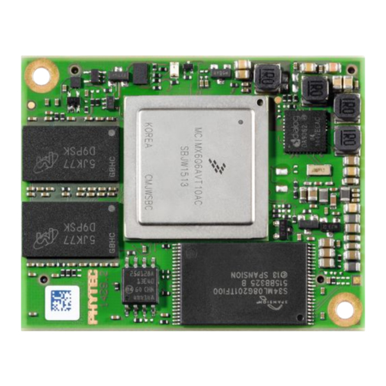
L-808e.A4 phyCORE-i.MX 6 Hardware Manual 3.2 Block Diagram FIGURE 1: Block Diagram of the phyCORE-i.MX 6 Note The specified direction indicated refers to the standard phyCORE use of the pin. © PHYTEC Messtecknik GmbH... - Page 16 L-808e.A4 phyCORE-i.MX 6 Hardware Manual 3.3 phyCORE-i.MX 6 Component Placement FIGURE 2: phyCORE‑i.MX 6 Component Placement (PCB 1429.3, top view) © PHYTEC Messtecknik GmbH...
- Page 17 L-808e.A4 phyCORE-i.MX 6 Hardware Manual FIGURE 3: phyCORE‑i.MX 6 Component Placement (PCB 1429.3, bottom view) Note The layout is identical for 1429.4 and 1429.5 except for some minor changes. 3.4 Minimum Requirements to Operate the phyCORE-i.MX 6 The basic operation of the phyCORE‑i.MX 6 only requires a supply of a +3.3 V input voltage with a typical 2.5 A load and the corresponding GND connection.
-
Page 18: Pin Description
L-808e.A4 phyCORE-i.MX 6 Hardware Manual 4 Pin Description Please note that all module connections are not to exceed their expressed maximum voltage or current. Maximum signal input values are indicated in the corresponding controller manuals/datasheets. As damage from improper connections varies according to use and application, it is the user's responsibility to take appropriate safety measures to ensure that the module connections are protected from overloading through connected peripherals. - Page 19 L-808e.A4 phyCORE-i.MX 6 Hardware Manual FIGURE 4: Pinout of the phyCORE-Connector (top view) Warning • The NXP® Semiconductor i.MX 6 is a multi-voltage operated microcontroller and as such special attention should be paid to the interface voltage levels to avoid unintentional damage to the microcontroller and other on-board components.
- Page 20 L-808e.A4 phyCORE-i.MX 6 Hardware Manual • Most of the controller pins have multiple multiplexed functions. As most of these pins are connected directly to the phyCORE-Connector the alternative functions are available by using the i.MX 6's pin muxing options. Signal names and descriptions in the tables below however are in regard to the specification of the phyCORE‑i.MX 6 and the functions defined Please refer to the...
- Page 21 L-808e.A4 phyCORE-i.MX 6 Hardware Manual TABLE 3: Pinout of the phyCORE-Connector X1, Row A Pin # Signal Signal Type Voltage Domain Description VDD_3V3 PWR_I 3.3 V 3.3 V Primary Voltage Supply Input VDD_3V3 PWR_I 3.3 V 3.3 V Primary Voltage Supply Input VDD_3V3 PWR_I 3.3 V...
- Page 22 L-808e.A4 phyCORE-i.MX 6 Hardware Manual X_UART3_CTS_B VDD_3V3_LOGIC UART3 clear to send output X_UART3_RTS_B VDD_3V3_LOGIC UART3 request to send input Ground 0 V X_ECSPI1_SCLK VDD_3V3_LOGIC eCSPI1 clock X_ECSPI1_MOSI VDD_3V3_LOGIC eCSPI1 master output/ slave input X_ECSPI1_SS0 VDD_3V3_LOGIC eCSPI1 chip select 0 [6][7] X_EIM_DA13...
- Page 23 L-808e.A4 phyCORE-i.MX 6 Hardware Manual X_CSI1_VSYNC VDD_3V3_LOGIC IPU2_CSI1 vertical synchronization X_CSI1_HSYNC VDD_3V3_LOGIC IPU2_CSI1 horizontal synchronization Ground 0 V X_EIM_BCLK VDD_3V3_LOGIC EIM burst block X_ECSPI2_MISO VDD_3V3_LOGIC eCSPI2 master input/ slave output X_ECSPI2_SS1 VDD_3V3_LOGIC eCSPI2 chip select 1 X_ECSPI2_SS0 VDD_3V3_LOGIC eCSPI2 chip select 0 Ground 0 V...
- Page 24 L-808e.A4 phyCORE-i.MX 6 Hardware Manual X_LCD_DATA03 VDD_3V3_LOGIC DISP0 data 3 X_LCD_DATA00 VDD_3V3_LOGIC DISP0 data 0 Ground 0 V X_LCD_ENABLE VDD_3V3_LOGIC DISP0 enable X_LCD_HSYNC VDD_3V3_LOGIC DISP0 horizontal synchronization X_LCD_RESET VDD_3V3_LOGIC DISP0 reset X_ENET_REFCLK VDD_3V3_LOGIC ENET RMII reference clock Ground 0 V X_ENET_TXER VDD_3V3_LOGIC...
- Page 25 L-808e.A4 phyCORE-i.MX 6 Hardware Manual TABLE 4: Pinout of the phyCORE-Connector X1, Row B Pin # Signal Signal Type Voltage Domain Description VDD_3V3 PWR_I 3.3 V 3.3 V Primary Voltage Supply Input VDD_3V3 PWR_I 3.3 V 3.3 V Primary Voltage Supply Input VDD_3V3 PWR_I 3.3 V...
- Page 26 L-808e.A4 phyCORE-i.MX 6 Hardware Manual X_ENET_MDIO VDD_ENET_IO ENET management data X_ENET_MDC VDD_ENET_IO ENET management data clock X_UART2_TX_DATA VDD_3V3_LOGIC UART2 serial transmit signal Ground 0 V X_I2C1_SCL OC_BI VDD_3V3_LOGIC I2C1 clock X_I2C1_SDA OC_BI VDD_3V3_LOGIC I2C1 data X_ECSPI1_MISO VDD_3V3_LOGIC eCSPI1 master input/ slave output...
- Page 27 L-808e.A4 phyCORE-i.MX 6 Hardware Manual Ground 0 V X_CSI1_DATA07 VDD_3V3_LOGIC IPU2_CSI1 data 7 X_CSI1_DATA06 VDD_3V3_LOGIC IPU2_CSI1 data 6 X_CSI1_DATA05 VDD_3V3_LOGIC IPU2_CSI1 data 5 X_CSI1_DATA04 VDD_3V3_LOGIC IPU2_CSI1 data 4 Ground 0 V [6][7] X_EIM_EB1 VDD_3V3_LOGIC EIM enable byte 1 X_ECSPI2_SCLK VDD_3V3_LOGIC eCSPI2 clock...
- Page 28 L-808e.A4 phyCORE-i.MX 6 Hardware Manual X_LCD_DATA07 VDD_3V3_LOGIC DISP0 data 7 X_LCD_DATA04 VDD_3V3_LOGIC DISP0 data 4 X_LCD_DATA02 VDD_3V3_LOGIC DISP0 data 2 X_LCD_DATA01 VDD_3V3_LOGIC DISP0 data 1 Ground 0 V X_LCD_CLK VDD_3V3_LOGIC DISP0 clock X_LCD_VSYNC VDD_3V3_LOGIC DISP0 vertical synchronization X_ENET_CRS_DV VDD_ENET_IO ENET RMII carrier sense/...
- Page 29 L-808e.A4 phyCORE-i.MX 6 Hardware Manual TABLE 5: Pinout of the phyCORE-Connector X1, Row C Pin # Signal Signal Type Voltage Domain Description X_BOOT_MODE0 VDD_3V3_LOGIC Boot mode input 0 X_ETH0_A+/TX0+ ETH_O VDD_3V3_LOGIC ETH0 data A+/transmit+ X_ETH0_A-/TX0- ETH_O VDD_3V3_LOGIC ETH0 data A-/transmit- Ground 0 V...
- Page 30 L-808e.A4 phyCORE-i.MX 6 Hardware Manual Ground 0 V X_CCM_CLKO2 VDD_3V3_LOGIC CCM clock output 2 X_USB_H1_DP USB_I/O i.MX 6 internal USB Host1 data+ X_USB_H1_DN USB_I/O i.MX 6 internal USB Host1 data- Ground 0 V X_PMIC_nSHUTDOWN VDD_3V3 PMIC shutdown X_3V3_GOOD VDD_MX6_SNVS 3V3 power good signal X_JTAG_TMS...
- Page 31 L-808e.A4 phyCORE-i.MX 6 Hardware Manual Ground 0 V X_HDMI_DDC_SDA VDD_3V3_LOGIC HDMI DDC data X_CSI0_DAT18 VDD_3V3_LOGIC IPU1_CSI0 data 18 X_CSI0_DAT16 VDD_3V3_LOGIC IPU1_CSI0 data 16 X_CSI0_DAT14 VDD_3V3_LOGIC IPU1_CSI0 data 14 Ground 0 V X_CSI0_DAT12 VDD_3V3_LOGIC IPU1_CSI0 data 12 X_CSI0_DAT10 VDD_3V3_LOGIC IPU1_CSI0 data 10 X_CSI0_DAT8...
- Page 32 L-808e.A4 phyCORE-i.MX 6 Hardware Manual X_LVDS0_TX3- LVDS_O i.MX 6 internal LVDS0 data 3- X_LVDS1_CLK+ LVDS_O i.MX 6 internal LVDS1 clock+ X_LVDS1_CLK- LVDS_O i.MX 6 internal LVDS1 clock- Ground 0 V X_LVDS1_TX0+ LVDS_O i.MX 6 internal LVDS1 data 0+ X_LVDS1_TX0- LVDS_O i.MX 6 internal LVDS1 data 0- 7.
- Page 33 L-808e.A4 phyCORE-i.MX 6 Hardware Manual TABLE 6: Pinout of the phyCORE-Connector X1, Row D Pin # Signal Signal Type Voltage Domain Description X_BOOT_MODE1 VDD_3V3_LOGIC Boot mode input 1 X_ETH0_B+/RX0+ ETH_I VDD_3V3_LOGIC ETH0 data B+/receive+ X_ETH0_B-/RX0- ETH_I VDD_3V3_LOGIC ETH0 data B-/receive-...
- Page 34 L-808e.A4 phyCORE-i.MX 6 Hardware Manual X_USB_OTG_OC VDD_3V3_LOGIC USB OTG overcurrent input X_USB_H1_VBUS PWR_I 5 V USB Host1 VBUS input X_JTAG_TCK VDD_3V3_LOGIC JTAG clock input Ground 0 V X_JTAG_TRSTB VDD_3V3_LOGIC JTAG reset input (low active) X_JTAG_TDI VDD_3V3_LOGIC JTAG TDI X_CSI_D1P CSI-2_I i.MX 6 internal...
- Page 35 L-808e.A4 phyCORE-i.MX 6 Hardware Manual Ground 0 V X_CSI0_DAT15 VDD_3V3_LOGIC IPU1_CSI0 data 15 X_CSI0_DAT13 VDD_3V3_LOGIC IPU1_CSI0 data 13 X_CSI0_DAT11 VDD_3V3_LOGIC IPU1_CSI0 data 11 X_CSI0_DAT9 VDD_3V3_LOGIC IPU1_CSI0 data 9 X_CSI0_DAT7 VDD_3V3_LOGIC IPU1_CSI0 data 7 X_CSI0_VSYNC VDD_3V3_LOGIC IPU1_CSI0 vertical synchronization Ground 0 V X_CSI0_DATA_EN...
- Page 36 L-808e.A4 phyCORE-i.MX 6 Hardware Manual Ground 0 V X_LVDS1_TX2+ LVDS_O i.MX 6 internal LVDS1 data 2+ X_LVDS1_TX2- LVDS_O i.MX 6 internal LVDS1 data 2- X_LVDS1_TX1+ LVDS_O i.MX 6 internal LVDS1 data 1+ X_LVDS1_TX1- LVDS_O i.MX 6 internal LVDS1 data 1- Ground 0 V X_LVDS1_TX3+ LVDS_O i.MX 6 internal...
- Page 37 L-808e.A4 phyCORE-i.MX 6 Hardware Manual 5 Jumpers For configuration purposes, the phyCORE‑i.MX 6 has several solder jumpers, some of which have been installed prior to delivery. Typical Jumper Pad Numbering Scheme illustrates the numbering of the solder jumper pads, while Jumper Locations (PCB 1429.3, top view) and Jumper Locations (PCB 1429.3, bottom view) indicate the location and the default configuration of the solder jumpers on the board.
- Page 38 L-808e.A4 phyCORE-i.MX 6 Hardware Manual FIGURE 6: Jumper Locations (PCB 1429.3 , top view) FIGURE 7: Jumper Locations (PCB 1429.3 , bottom view) © PHYTEC Messtecknik GmbH...
- Page 39 L-808e.A4 phyCORE-i.MX 6 Hardware Manual Note The layout is identical for 1429.4 and 1429.5 except for some minor changes. Please pay special attention to the “TYPE” column to ensure you are using the correct type of jumper (0 Ohms, 10k Ohms, etc…).
- Page 40 L-808e.A4 phyCORE-i.MX 6 Hardware Manual TABLE 7: Jumper Settings Jumper Description Type Section J4 connects the write-protect input of the onboard EEPROM with GND. If this jumper is not populated, the EEPROM is write-protected. 0R (0402) EEPROM Write Protection Control (J4)
- Page 41 L-808e.A4 phyCORE-i.MX 6 Hardware Manual 6 Power The phyCORE‑i.MX 6 operates off of a single power supply voltage. The following sections of this chapter discuss the primary power pins on the phyCORE‑Connector X1 in detail. 6.1 Primary System Power (VDD_3V3) The phyCORE‑i.MX 6 operates off of a primary voltage supply with a nominal value of +3.3 V.
- Page 42 L-808e.A4 phyCORE-i.MX 6 Hardware Manual 6.2.1 Power Domains External voltages: • VDD_3V3 3 V main supply voltage • USB0_VBUS USB0 Bus voltage must be supplied with 5 V if USB0 is used • USB1_VBUS USB1 Bus voltage must be supplied with 5 V if USB1 is used •...
- Page 43 L-808e.A4 phyCORE-i.MX 6 Hardware Manual FIGURE 8: Powering Scheme of the phyCORE- i.MX 6 6.3 Supply Voltage for External Logic The voltage level of the phyCORE’s logic circuitry is VDD_3V3_LOGIC (3.3 V), derived from the SOM's main input voltage VDD_3V3. In order to follow the power-up and power-down sequencing mandatory for the i.MX 6 external devices must be supplied by the I/O supply voltage VDD_3V3_LOGIC which is brought out at pin X1B5 of the phyCORE-Connector.
- Page 44 L-808e.A4 phyCORE-i.MX 6 Hardware Manual The use of level shifters supplied with VDD_3V3_LOGIC allows converting the signals according to the needs of the custom target hardware. Alternatively, signals can be connected to an open drain circuitry with a pull-up resistor attached to VDD_3V3_LOGIC.
- Page 45 L-808e.A4 phyCORE-i.MX 6 Hardware Manual 7 Reset Pin X1D32 on the phyCORE‑Connector is designated as reset input/output. If used as reset input a hard reset of the module can be triggered. In this case, the external reset signal is connected to the nRESETREQ signal of the DA9062 PMIC which triggers a hard reset of the module with a debouncing time of 10.24 ms.
-
Page 46: System Configuration And Booting
L-808e.A4 phyCORE-i.MX 6 Hardware Manual 8 System Configuration and Booting Although most features of the i.MX 6 microcontroller are configured and/or programmed during the initialization routine, other features, which impact program execution, must be configured prior to initialization via pin termination. - Page 47 Please refer to the i.MX 6 Reference Manual for further information about the eFUSEs and the impact of the settings at the BCFG pins. 11. For series production, PHYTEC offers the phyCORE‑i.MX 6 with a custom configuration of the eFUSEs. ...
- Page 48 L-808e.A4 phyCORE-i.MX 6 Hardware Manual TABLE 10: Boot Configuration Pins at the phyCORE‑Connector Configuration Pin Pin # Signal Signal Type Signal Level Description BCFG1[0] X1A30 X_CSI1_DATA09 3.3 V IPU2_CSI1 data 9 BCFG1[1] X1A32 X_CSI1_DATA08 3.3 V IPU2_CSI1 data 8 BCFG1[2] X1B39 X_CSI1_DATA07 3.3 V...
- Page 49 L-808e.A4 phyCORE-i.MX 6 Hardware Manual BCFG3[3] X1B35 X_CSI1_DATA14 3.3 V IPU2_CSI1 data 14 BCFG3[4] X1B34 X_CSI1_DATA15 3.3 V IPU2_CSI1 data 15 BCFG3[5] X1B32 X_CSI1_DATA16 3.3 V IPU2_CSI1 data 16 BCFG3[6] X1B31 X_CSI1_DATA17 3.3 V IPU2_CSI1 data 17 BCFG3[7] X1B30 X_CSI1_DATA18 3.3 V IPU2_CSI1 data 18...
-
Page 50: System Memory
The following sections of this chapter detail each memory type used on the phyCORE‑i.MX 6. 1. The maximum memory size listed is as of the printing of this manual. Please contact PHYTEC for more information about additional, or new module configurations available. 9.1 DDR3-SDRAM (U4-U7) The RAM memory of the phyCORE‑i.MX 6 is comprised of one 64-bit wide bank with four 16-bit wide DDR3-SDRAM... - Page 51 L-808e.A4 phyCORE-i.MX 6 Hardware Manual 9.3 eMMC Flash Memory (U14) Alternatively to the NAND flash memory at U12, an eMMC can be populated at U14. The eMMC device is programmable with 3.3 V. No dedicated programming voltage is required. The eMMC Flash memory is connected to the SD4 interface of the i.MX 6.
- Page 52 L-808e.A4 phyCORE-i.MX 6 Hardware Manual 9.5 SPI Flash Memory (U9) The SPI Flash Memory of the phyCORE‑i.MX 6 at U9 can be used to store configuration data or any other general- [14] [14] purpose data. Besides this, it can also be used as a boot device and recovery boot device .
- Page 53 L-808e.A4 phyCORE-i.MX 6 Hardware Manual 10 SD/MM Card Interfaces The phyCORE bus features two SD/MM Card interfaces. On the phyCORE‑i.MX 6, the interface signals extend from the controller's third and first Ultra Secured Digital (uSDHC3 / uSDHC1) Host Controller to the phyCORE- Connector. Location of the SD/MM Card Interface Signals...
- Page 54 L-808e.A4 phyCORE-i.MX 6 Hardware Manual X1B15 X_SD1_DATA1 VDD_3V3_LOGIC uSDHC1 data 1 X1B16 X_SD1_DATA3 VDD_3V3_LOGIC uSDHC1 data 3 The interfaces do not provide dedicated card-detect or write-protect signals. The card detects and write-protect function can be implemented easily by using four GPIOs of the i.MX 6.
-
Page 55: Serial Interfaces
L-808e.A4 phyCORE-i.MX 6 Hardware Manual 11 Serial Interfaces The phyCORE‑i.MX 6 provides numerous dedicated serial interfaces some of which are equipped with a transceiver to allow direct connection to external devices: 2x high-speed UARTs (TTL, derived from UART2 and UART3 of the i.MX 6) with up to 4 MHz and one with hardware flow control (RTS and CTS signals) 1x High-speed USB OTG interface (extended directly from the i.MX 6’s USB OTG PHY (USBPHY1)) -
Page 56: Usb Otg Interface
L-808e.A4 phyCORE-i.MX 6 Hardware Manual 5. Special care must be taken not to override the device configuration when using this pin as input (Boot Device Selection and Configuration). 11.2 USB OTG Interface The phyCORE‑i.MX 6 provides a high-speed USB OTG interface that uses the i.MX 6 embedded HS USB OTG PHY. An external USB Standard-A (for USB host), USB Standard-B (for USB device), or USB mini-AB (for USB OTG) connector is all that is needed to interface the phyCORE‑i.MX 6 USB OTG functionality. -
Page 57: Usb Host Interface
L-808e.A4 phyCORE-i.MX 6 Hardware Manual 11.3 USB Host Interface The phyCORE‑i.MX 6 provides a high-speed USB host interface that uses the i.MX 6 embedded HS USB host PHY. An external USB Standard-A (for USB host) connector is all that is needed to interface the phyCORE‑i.MX 6 USB host functionality. - Page 58 L-808e.A4 phyCORE-i.MX 6 Hardware Manual X1C7 X_ETH0_LED0 VDD_3V3_LOGIC ETH0 link LED output X1D2 X_ETH0_B+/RX0+ ETH_I VDD_3V3_LOGIC ETH0 data B+/receive+ X1D3 X_ETH0_B-/RX0- ETH_I VDD_3V3_LOGIC ETH0 data B-/receive- X1D4 X_ETH0_LED1 VDD_3V3_LOGIC ETH0 traffic LED output X1D5 X_ETH0_D+ ETH_I/O VDD_3V3_LOGIC ETH0 data D+ (only GbE)
- Page 59 L-808e.A4 phyCORE-i.MX 6 Hardware Manual In order to guarantee that the MAC address is unique, all addresses are managed in a central location. PHYTEC has acquired a pool of MAC addresses. The MAC address of the phyCORE‑i.MX 6 is located on the bar code sticker attached to the module.
-
Page 60: Spi Interface
L-808e.A4 phyCORE-i.MX 6 Hardware Manual X1B69 X_ENET_TXD0 VDD_ENET_IO ENET RMII transmit data X1B70 X_ENET_TXD1 VDD_ENET_IO ENET RMII transmit data 11.5 SPI Interface The Serial Peripheral Interface (SPI) interface is a four-wire, bidirectional serial bus that provides a simple and efficient method for data exchange among devices. The phyCORE provides two SPI interfaces on the phyCORE‑Connector X1. - Page 61 L-808e.A4 phyCORE-i.MX 6 Hardware Manual 5. Special care must be taken not to override the device configuration when using this pin as input (Boot Device Selection and Configuration). Note When using the eCSPI1 interface it must be considered that the on-board SPI Flash is connected to this interface, too.
- Page 62 L-808e.A4 phyCORE-i.MX 6 Hardware Manual 11.7 I S Audio Interface (SSI) The Synchronous Serial Interface (SSI) of the phyCORE‑i.MX 6 is a full-duplex serial interface that allows communication with a variety of serial devices, such as standard codecs, digital signal processors (DSPs), microprocessors, peripherals, and popular industry audio codecs that implement the Inter-IC sound bus standard S) and Intel AC’97 standard.
-
Page 63: Can Interface
L-808e.A4 phyCORE-i.MX 6 Hardware Manual 11.8 CAN Interface The CAN interface of the phyCORE‑i.MX 6 is connected to the first FlexCAN module (FlexCAN1) of the i.MX 6 which is a full implementation of the CAN protocol specification Version 2.0B. It supports standard and extended message frames and programmable bit rates of up to 1 Mb/s. -
Page 64: Pci Express Interface
Additional control signals which might be required (e.g. “present” and “wake”) can be implemented with GPIOs. Please refer to the schematic of a suitable PHYTEC carrier board (e.g. phyBOARD‑Mira i.MX 6) for a circuit example. The table shows the position of the PCIe signals on the phyCORE‑Connector X1. -
Page 65: General Purpose I/Os
L-808e.A4 phyCORE-i.MX 6 Hardware Manual 12 General Purpose I/Os The table below lists all pins not used by any other of the interfaces described explicitly in this manual and which therefore can be used as GPIO without harming other features of the phyCORE‑i.MX 6. - Page 66 L-808e.A4 phyCORE-i.MX 6 Hardware Manual 13 User-programmable LED The phyCORE‑i.MX 6 provides one green user-programmable LED (D1) on board. It can be controlled by setting GPIO1_04 to the desired output level. A high-level turns the LED on, a low-level turns it off.
-
Page 67: Debug Interface
L-808e.A4 phyCORE-i.MX 6 Hardware Manual 14 Debug Interface The phyCORE‑i.MX 6 is equipped with a JTAG interface for downloading program code into the external flash, internal controller RAM, or for debugging programs currently executing. The table below shows the location of the JTAG pins on the phyCORE-Connector X1. -
Page 68: Parallel Display Interface
L-808e.A4 phyCORE-i.MX 6 Hardware Manual 15 Display Interfaces 15.1 Parallel Display Interface The signals from the LCD interface of the i.MX 6 are brought out at phyCORE‑Connector X1. Thus an LCD interface with up to 24-bit bus width can be connected directly to the phyCORE‑i.MX 6. The table below shows the location of the applicable interface signals. - Page 69 L-808e.A4 phyCORE-i.MX 6 Hardware Manual X1B50 X_LCD_DATA20 VDD_3V3_LOGIC DISP0 data 20 X1B51 X_LCD_DATA18 VDD_3V3_LOGIC DISP0 data 18 X1B52 X_LCD_DATA17 VDD_3V3_LOGIC DISP0 data 17 X1B54 X_LCD_DATA15 VDD_3V3_LOGIC DISP0 data 15 X1B55 X_LCD_DATA12 VDD_3V3_LOGIC DISP0 data 12 X1B56 X_LCD_DATA10 VDD_3V3_LOGIC DISP0 data 10...
- Page 70 L-808e.A4 phyCORE-i.MX 6 Hardware Manual X1C64 X_LVDS0_TX3+ LVDS_O i.MX 6 internal LVDS0 data 3+ X1C65 X_LVDS0_TX3- LVDS_O i.MX 6 internal LVDS0 data 3- X1D58 X_LVDS0_CLK+ LVDS_O i.MX 6 internal LVDS0 clock+ X1D59 X_LVDS0_CLK- LVDS_O i.MX 6 internal LVDS0 clock- X1D60 X_LVDS0_TX2+ LVDS_O i.MX 6 internal...
-
Page 71: High-Definition Multimedia Interface (Hdmi)
L-808e.A4 phyCORE-i.MX 6 Hardware Manual 16 High-Definition Multimedia Interface (HDMI) The High-Definition Multimedia Interface (HDMI) of the phyCORE‑i.MX 6 is compliant with HDMI 1.4 and DVI 1.0. It supports a maximum pixel clock of up to 340 MHz for up to 720p at 100 Hz and 720i at 200 Hz, or 1080p at 60 Hz and 1080i/720i at 120 Hz HDTV display resolutions and a graphic display resolution of up to 2048x1536 (QXGA). -
Page 72: Camera Interfaces
All signals (including control signals and an I C interface) to use the camera interfaces according to PHYTEC's phyCAM‑S+, or phyCAM‑P standard are available at the phyCORE‑Connector. The i.MX 6 (Solo), and i.MX 6 (DualLite) microcontrollers are equipped with one parallel camera port (IPU1_CSI0) - Page 73 L-808e.A4 phyCORE-i.MX 6 Hardware Manual FIGURE 12: Camera Interfaces at the phyCORE‑Connector (Parallel 0(CSI0 of IPU#1), Parallel 1(CSI1 of IPU#2), and MIPI CSI-2) The camera interfaces of the phyCORE‑i.MX 6 include all signals and are prepared to be used as phyCAM‑S(+), phyCAM‑P, or MIPI CSI-2 interface on an appropriate carrier board.
- Page 74 L-808e.A4 phyCORE-i.MX 6 Hardware Manual X1D44 X_CSI0_DAT13 VDD_3V3_LOGIC IPU1_CSI0 data 13 X1C49 X_CSI0_DAT12 VDD_3V3_LOGIC IPU1_CSI0 data 12 X1D45 X_CSI0_DAT11 VDD_3V3_LOGIC IPU1_CSI0 data 11 X1C50 X_CSI0_DAT10 VDD_3V3_LOGIC IPU1_CSI0 data 10 X1D46 X_CSI0_DAT9 VDD_3V3_LOGIC IPU1_CSI0 data 9 X1C51 X_CSI0_DAT8 VDD_3V3_LOGIC IPU1_CSI0 data 8...
- Page 75 16. Recommended to implement special control features for the camera interface circuitry on the carrier board (e.g. enabling/disabling of the interface, switching between phyCAM-P and phyCAM-S, etc.). Please refer to L-748 or appropriate PHYTEC CB designs as reference. Using the phyCORE's camera interface Parallel 0, together with an I²C bus facilitates easy implementation of a CMOS camera interface, e.g.
- Page 76 L-808e.A4 phyCORE-i.MX 6 Hardware Manual 17.2 Parallel 1 Camera Interface (CSI1 of IPU#2) The camera interface Parallel 1 (CSI1 of IPU#2) is available at the phyCORE‑Connector with 20 data bits, HSYNC, VSYNC, and PIXCLK. The following table shows the location of the Parallel 1 (CSI1 of IPU#2) camera signals at the phyCORE‑Connector.
-
Page 77: Mipi Csi-2 Camera Interface
16. Recommended to implement special control features for the camera interface circuitry on the carrier board (e.g. enabling/disabling of the interface, switching between phyCAM-P and phyCAM-S, etc.). Please refer to L-748 or appropriate PHYTEC CB designs as reference. 17.3 MIPI CSI-2 Camera Interface The MIPI CSI-2 camera interface of the i.MX 6 extends to the phyCORE‑Connector X1 with 4 data lanes and one clock... - Page 78 Using the I²C bus and the camera clock signal allows a MIPI CSI-2 camera module to connect directly. 17.4 Utilizing the Camera Interfaces on a Carrier Board On PHYTEC carrier boards, the interfaces are used directly as parallel interfaces according to the phyCAM-P standard (Use of Parallel 0 (CSI0 of IPU#1) and Parallel 1 (CSI1 of IPU#2) as phyCAM‑P...
- Page 79 FIGURE 14: Use of Parallel 0 (CSI0 of IPU#1) and Parallel 1 (CSI1 of IPU#2) as phyCAM‑S+ Interface More information on the PHYTEC camera interface standards phyCAM‑P and phyCAM-S+ and how to implement them on a custom carrier board can be found in the corresponding manual L-748. The schematics of the phyBOARD‑Mira i.MX 6 on which camera interface Parallel 0 is brought out as a phyCAM‑S+ interface (LVDS) can also...
-
Page 80: Tamper Detection
L-808e.A4 phyCORE-i.MX 6 Hardware Manual 18 Tamper Detection The phyCORE-i.MX 6 supports the tamper detection feature of the i.MX 6. With the tamper detection feature, it is possible to recognize when the device encounters unauthorized opening or tampering. For this purpose, i.MX 6's Tamper Detection signal is available at pin X1D70 of the phyCORE‑Connector. -
Page 81: Technical Specifications
L-808e.A4 phyCORE-i.MX 6 Hardware Manual 19 Technical Specifications FIGURE 15: Physical Dimensions (top view) The physical dimensions of the phyCORE‑i.MX 6 are represented in Physical Dimensions (top view). The module’s profile is max. 10 mm thick, with a maximum component height of 3.0 mm on the bottom (connector) side of the PCB and approximately 5.0 mm on the top (microcontroller) side. - Page 82 L-808e.A4 phyCORE-i.MX 6 Hardware Manual Operating Voltage: VCC 3.3 V +/- 5 % Power Consumption: Linux prompt only: typical 1.9 W QT Demo: typical 4.1 W 4 Cores full load + QT Demo: typical 6 W Conditions: 1 GB DDR3-SDRAM, 1 GB NAND Flash, Ethernet, Quad-core 1 GHz CPU frequency, 20 °C, 3.3 V...
- Page 83 L-808e.A4 phyCORE-i.MX 6 Hardware Manual Industrial -40 °C to Industrial Industrial +105 °C / -40 °C to +95 °C -40 °C to +85 °C Automotive -40 °C to+125 °C Extended Commercial Industrial Industrial -20 °C to +105 °C -40 °C to +95 °C -40 °C to +85 °C Commercial 0 °C to +95 °C Consumer Consumer 0 °C to +95 °C...
- Page 84 L-808e.A4 phyCORE-i.MX 6 Hardware Manual Please refer to the corresponding data sheets and mechanical specifications provided by Samtec (www.samtec.com). © PHYTEC Messtecknik GmbH...
- Page 85 L-808e.A4 phyCORE-i.MX 6 Hardware Manual 20 Hints for Integrating and Handling the phyCORE-i.MX 6 20.1 Integrating the phyCORE-i.MX 6 • Design Rule Successful integration in user target circuitry greatly depends on the adherence to the layout design rules for the GND connections of the phyCORE module.
- Page 86 L-808e.A4 phyCORE-i.MX 6 Hardware Manual FIGURE 16: phyCORE-iMX 6 Footprint © PHYTEC Messtecknik GmbH...
-
Page 87: Revision History
L-808e.A4 phyCORE-i.MX 6 Hardware Manual 21 Revision History TABLE 38: Date Version numbers Changes in this manual 04.06.2015 Manual First edition. L-808e_1 Describes the phyCORE‑i.MX 6 PCB‑Version 1429.1 04.08.2016 Manual Second edition. L-808e_2 Describes the phyCORE‑i.MX 6 PCB‑Version 1429.2 and 1429.3 04.08.2016 Manual Third edition.
Need help?
Do you have a question about the L-808e.A4 and is the answer not in the manual?
Questions and answers