
Related Manuals for Phytec microMODUL-8051


Summary of Contents for Phytec microMODUL-8051
- Page 1 Hardware-Manual Edition April 1999 A product of a PHYTEC Technology Holding company...
- Page 2 © Copyright 1999 PHYTEC Meßtechnik GmbH. rights - including those of translation, reprint, broadcast, photomechanical or similar reproduction and stor- age or processing in computer systems, in whole or in part - are reserved. No...
-
Page 3: Table Of Contents
3.2 Serial Interface J2, J3..............12 Memory-model...................13 4.1 Control Register 1...............15 4.2 Control Register 2...............20 4.3 Address Register.................21 4.4 Mask Register ................22 Flash-Memory..................25 Battery Buffer ..................27 Technical Specifications..............29 Hints for Handling the Module ............31 Index ......................33 © PHYTEC Meßtechnik GmbH 1999 L-168e_5... - Page 4 Figure 8: Memory Areas of the Flash Device..........25 Figure 9: Physical Dimensions ..............29 Table 1: Pinout of the microMODUL-Connector ........6 Table 2: Reserved Pins ................7 Table 3: Jumper Settings ................10 © PHYTEC Meßtechnik GmbH 1999 L-168e_5...
-
Page 5: Preface
Declaration regarding EMV-Conformity of the PHYTEC microMODUL-8051 PHYTEC Single Board Computers (henceforth products) are designed for installation in electrical appliances or as dedicated Evaluation Boards (i.e.: for use as a test and prototype platform for hardware/software development) in laboratory environments. - Page 6 PHYTEC supports all common 8- and 16-bit controllers in two ways: as the basis for Starter Kits in which user-designed hardware can be implemented on a wrap-field around the controller and as insert-ready, fully functional micro- and miniMODULS which can be embedded directly into the user’s peripheral...
-
Page 7: Introduction
255 nodes in an ARCnet network. Precise specifications for the specific controller fitted on the microMODUL-8051 you have purchased can be found in the enclosed microcontroller manual. The microMODUL-8051 described herein is based on the standard 80C32 architecture. There follows no specific discussion of 80C32-derivative controllers, as the architecture of these derivatives is not relevant to the basic functioning of this module. - Page 8 The microMODUL-8051 offers the following features: • SBC in matchbox-size dimensions (51 x 36 mm) achieved through modern SMD technology • improved interference safety through multi-layer technology • controller signals and ports extend to standard-width (2.54 mm.) pins aligning board edges, allowing the board to be plugged into any target application like a “big chip”...
-
Page 9: Pin-Layout
Table 1 provides an overview of the pinout of the microMODUL- Connector, as well as hints about additional functions of some of the port pins. For further details please refer to the Data Sheet of the controller on the microMODUL-8051. © PHYTEC Meßtechnik GmbH 1999 L-168e_5... - Page 10 Reserved 4 Pin 1 (PLCC) / 39 (QFP) of the controllers (the function is dependent upon the controller derivative, see below) 45...52 A8...A15 Address bus (High-Byte) Table 1: Pinout of the microMODUL-Connector © PHYTEC Meßtechnik GmbH 1999 L-168e_5...
- Page 11 DS80C320 n.c. n.c. n.c. n.c. C501 n.c. n.c. n.c. n.c. C502 n.c. n.c. n.c. n.c. C504 COUT3 /CTRAP VAREF VAGND COM20051 TXEN /PULSE1 /PULSE2 RXIN Table 2: Reserved Pins n.c.= not connected © PHYTEC Meßtechnik GmbH 1999 L-168e_5...
- Page 12 © PHYTEC Meßtechnik GmbH 1999 L-168e_5...
-
Page 13: Jumpers
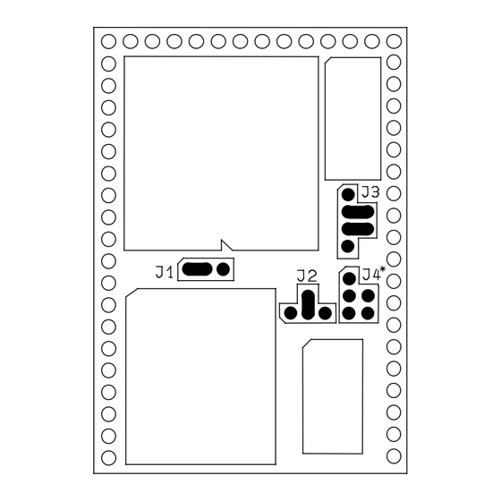
Figure 2 illustrates the numbering of the Jumper-pads, while Figure 3 indicates the location of the Jumpers on the board. . All soldering jumpers on the microMODUL-8051 are located on its top side. Figure 2: Numbering of the Jumper-pads... -
Page 14: Special Features J1, J4
2+3 on Jumper J1 must be connected. The following configurations are possible: Code-Fetch execution from external pro- gram memory execution from internal pro- gram memory © PHYTEC Meßtechnik GmbH 1999 L-168e_5... - Page 15 For others than the listed controllers, the circuit diagram of the microMODUL-8051 and the pinout of such controllers will specify the settings of the respective Jumpers which enable external peripheral connectivity. This could necessitate that required - but unassigned - signals have to be conducted externally via the reserved module pins (10, 42...44).
-
Page 16: Serial Interface J2, J3
3.2 Serial Interface J2, J3 With Jumpers J2 and J3 different signal levels and signal qualities can be applied to the serial interface pins of the microMODUL-8051 (Pins 35 and 36). These pins carry either the TTL-signals of the controller’s serial interface, the signals of the on-board RS-232 transceiver or the signals of the on-board RS-485 transceiver. -
Page 17: Memory-Model
Hardware-RESET erases all registers, while preserving the configuration of the default memory. In the event that you use the FlashTools – PHYTEC’S proprietary firmware allowing convenient on-board Flash-programming - it should be noted that the address FA16 will be preset at the start of your application software (refer to the section 4.1 'Control... -
Page 18: Figure 4: Default-Memory-Model After Hardware-Reset
8000H - FFFFH. The corresponding current I/O-area is concentrated in an XDATA-address area in which there is no access to any existing RAM. In the following sections the registers of the address decoder for configuration of the memory are explained: © PHYTEC Meßtechnik GmbH 1999 L-168e_5... -
Page 19: Control Register 1
This is to be noted upon installation of the software copy of the register contents. PHYTEC firmware allowing convenient on-board Flash-programming. Upon delivery of the module, this firmware is already resident in the Flash device © PHYTEC Meßtechnik GmbH 1999... -
Page 20: Figure 5: Memory-Model For Flash-Programming
I/O-area is located in the address area from 7C00H to 7FFFH. This I/O-area generally consists of 4 blocks of 256 bytes. In three of these blocks the address decoder provides precoded Chip-Select-Signal which simplifies the connection of peripheral hardware to the module. © PHYTEC Meßtechnik GmbH 1999 L-168e_5... -
Page 21: Figure 6: Partitioning Of The I/O-Area
7FFFH / FFFFH /CS3 7F00H / FF00H 7EFFH / FEFFH /CS2 7E00H / FE00H 7DFFH / FDFFH /CS1 7D00H / FD00H 7CFFH / FCFFH /CS-REG 7C00H / FC00H Write-Only Read-Write Figure 6: Partitioning of the I/O-Area © PHYTEC Meßtechnik GmbH 1999 L-168e_5... - Page 22 Runtime-model (PRG-EN = 0). In the Program- ming-model (PRG=1) it is unimportant and ignored. PHYTEC firmware allowing convenient on-board Flash-programming. Upon delivery of the module, this firmware is already resident in the Flash device Memory area in which no difference is made between CODE- and XDATA-access.
- Page 23 Flash. Bits FA[18..16] are dependent on the hardware configuration of the module and function as described above only if Flash devices of at least 512 kByte are used on the board. © PHYTEC Meßtechnik GmbH 1999 L-168e_5...
-
Page 24: Control Register 2
RAM devices of at least 128 kByte. N/A: Not Accessible Reserved bits are not to be changed, the default value (0) has to remain. © PHYTEC Meßtechnik GmbH 1999 L-168e_5... -
Page 25: Address Register
Memory area in which CODE and XDATA-accesses use different physical memory devices. Usually CODE-access uses a ROM or Flash device, whereas XDATA-access uses a RAM. Reserved bits are not to be changed, the default value (0) must remain. © PHYTEC Meßtechnik GmbH 1999 L-168e_5... -
Page 26: Mask Register
0000H to 7FFFH. This should be taken into consideration when choosing the memory- model. Otherwise, function failure could result from overlapping access. Reserved bits are not to be changed, the default value (0) has to remain. © PHYTEC Meßtechnik GmbH 1999 L-168e_5... - Page 27 10100X00 b 00000100b Harvard A000H-A7FFH, Von-Neumann 0000H-9FFFH and A800H-FFFFH Reserved bits without function for address decoding (refer to description of the register) X = irrelevant (on account of a bit set in the mask register) © PHYTEC Meßtechnik GmbH 1999 L-168e_5...
-
Page 28: Figure 7: Example Of A Memory-Model
A7FFH Flash U7 Harvard A000H 9FFFH Von-Neumann RAM U2 0000H PRG-EN = 0 VN-EN = 1 IO-SW = 0 RAM-SW = 0 Addr.-Reg. = 10100X00b Mask.-Reg. = 00000100b Figure 7: Example of a Memory-model © PHYTEC Meßtechnik GmbH 1999 L-168e_5... -
Page 29: Flash-Memory
5 Flash-Memory Flash is a highly functional means of storing non-volatile data. Having the microMODUL-8051 equipped with a Flash device makes this modern technique available. The microMODUL-8051 can house a Flash device of type 29F010 with two banks of 64 kByte each or of type 29F040 with 8 banks of 64kByte each. - Page 30 Flash (such as into von-Neumann RAM). This usually equals the interruption of a "normal" program execution cycle. As of the printing of this manual, Flash devices generally have a life expectancy of at least 100,000 Erase-/Program-cycles. © PHYTEC Meßtechnik GmbH 1999 L-168e_5...
-
Page 31: Battery Buffer
Technical Specification 6 Battery Buffer The battery that buffers the memory is not otherwise essential to the functioning of the microMODUL-8051. However, this battery buffer embodies an economical and practical means of storing nonvolatile data. The VBAT-input at pin 41 is intended to connect to an external battery. - Page 32 © PHYTEC Meßtechnik GmbH 1999 L-168e_5...
-
Page 33: Technical Specifications
_______________________________________________________________________ 7 Technical Specifications The physical dimensions of the microMODUL-8051 are represented in Figure 9. The module’s profile is about 10 mm thick, with a max. height of the components of 3.5 mm on the back-side of the board and approx. - Page 34 RAM-device at +20°C This specifications describe the standard configuration of the microMODUL-8051 as of the pressing of this manual. Please note that utilizing the battery buffer for the RAMs the storage temperature is only 0°C to +70°C.
-
Page 35: Hints For Handling The Module
Carefully heat neighboring connections in pairs. After a few alternations, components can be removed with the solder-iron tip. Alternatively, a hot air gun can be used to heat and loosen the bonds. © PHYTEC Meßtechnik GmbH 1999 L-168e_5... - Page 36 © PHYTEC Meßtechnik GmbH 1999 L-168e_5...
-
Page 37: Index
FA[18..15] .........19 ..........14 Features ........4 RS-232 Transceiver....12 Flash-Memory ......25 RS-485 Transceiver....12 Hints for Handling the Module .31 Serial Interface ......12 Special Features......10 Interface........12 IO-SW ........16 Technical Specifications....29 J1 10 VN-EN........18 J2 12 J3 12 © PHYTEC Meßtechnik GmbH 1999 L-168e_5... - Page 38 © PHYTEC Meßtechnik GmbH 1999 L-168e_5...
- Page 39 How would you improve this manual? Did you find any mistakes in this manual? page Submitted by: Customer number: Name: Company: Address: Return to: PHYTEC Technologie Holding AG Postfach 100403 D-55135 Mainz, Germany Fax : +49 (0) 6131 9221-33 © PHYTEC Meßtechnik GmbH 1999 L-168e_5...
- Page 40 Published by © PHYTEC Meßtechnik GmbH 1999 Ordering No. L-168e_5 Printed in Germany...
Need help?
Do you have a question about the microMODUL-8051 and is the answer not in the manual?
Questions and answers