
Related Manuals for Phytec phyCORE-i.MX RT1170


Summary of Contents for Phytec phyCORE-i.MX RT1170
- Page 1 ® phyCORE -i.MX RT1170 Hardware Manual Document No.: L-1064e.A0 SOM Prod. No.: PCM-073 SOM PCB. No.: 1569.0 CB Prod. No.: PBA-C-26 CB PCB. No.: 1570.0 Edition: Dec 2023 A product of a PHYTEC Technology Holding company...
-
Page 2: Table Of Contents
4.10.2 General Signal Routing Guidelines ..................... 37 Power ............................... 37 Primary System Power (VIN) ......................37 5.1.1 Primary Power Reference Circuit ....................38 Backup Power (V_BATT) ........................40 Reset ..............................40 Power Sequencing ..........................41 © PHYTEC America L.L.C. 2023... - Page 3 FlexIO Pinout ..........................65 C ..............................66 7.4.1 C Pinout ..........................67 LPSPI ..............................67 7.5.1 LPSPI Pinout ..........................68 LPUART ............................69 7.6.1 LPUART Pinout .......................... 69 USB ..............................72 7.7.1 USB Pinout ..........................72 © PHYTEC America L.L.C. 2023...
- Page 4 Power Gating and Memory Controller ....................84 9.3.1 PGMC Pinout ..........................84 10 Peripheral Interfaces ..........................84 10.1 ACMP ..............................84 10.1.1 ACMP Pinout ..........................85 10.2 ADC ..............................85 10.2.1 ADC Pinout ..........................85 © PHYTEC America L.L.C. 2023...
- Page 5 JTAG Pinout ..........................102 11.1.2 JTAG Reference Circuit ......................102 11.2 ARM Debug and Trace ........................103 11.2.1 ARM Pinout ..........................103 11.3 LPUART1 ............................103 11.3.1 LPUART1 Pinout ........................103 11.3.2 LPUART1 Reference Circuits ....................104 © PHYTEC America L.L.C. 2023...
- Page 6 13 Integrating and Updating the phyCORE-I.MXRT1170 ................108 13.1 Integration ............................108 13.2 Modification ............................. 108 13.3 In-Field Updates ..........................108 13.4 Product Change Management ......................109 14 Additional Information ..........................110 15 Revision History ............................. 112 © PHYTEC America L.L.C. 2023...
-
Page 7: List Of Figures
Figure 30. MIPI-DSI Connector Reference Schematic ................. 79 Figure 31. MIPI-CSI Power Toggle Reference Schematic ................81 Figure 32. MIPI-CSI Connector Reference Schematic ................. 82 Figure 33. JTAG Reference Schematic ...................... 102 Figure 34. UART0 to USB Bridge Reference Schematic ................104 © PHYTEC America L.L.C. 2023... -
Page 8: List Of Tables
Table 29 USB Connections at the phyCORE-Connector ................72 Table 30 phyCORE-I.MXRT1170 USB0 Layout Characteristics ..............72 Table 31 SAI Connections at the phyCORE-Connector ................73 Table 32 SPDIF Connections at the phyCORE-Connector ................75 © PHYTEC America L.L.C. 2023... - Page 9 Table 65 ARM Connections at the phyCORE-Connector ................103 Table 66 LPUART1 Connections at the phyCORE-Connector ..............103 Table 67 MAIN Connections at the phyCORE-Connector ................. 106 Table 68 MCU Connections at the phyCORE-Connector ................106 © PHYTEC America L.L.C. 2023...
- Page 10 PCM-073/phyCORE-i.MXRT1170 System on Module L-1064e.A0 Table 69 SNVS Connections at the phyCORE-Connector ................ 106 Table 70 Document Revision History ......................112 © PHYTEC America L.L.C. 2023...
-
Page 11: Som Features
1x PDM (Pulse Density Modulation) module • 1x PGMC (Power Gating and Memory Controller) module • 2x PIT (Periodical Interrupt Timer) modules • 4x SAI (Synchronous Audio Interface) modules • 1x SNVS (Secure Non-Volatile Storage) module © PHYTEC America L.L.C. 2023... -
Page 12: Conventions, Abbreviations And Acronyms
The PHYTEC provided SDK includes drivers and/or software for controlling all components such as interfaces, memory, etc. Therefore, programming close to the hardware (at the register level) is not necessary in most cases. For this reason, this manual contains no detailed description of the processor's registers, or information relevant for software development. -
Page 13: Abbreviations And Acronyms
Liquid Crystal Display Printed circuit board Peripheral Component Interconnect Product Change Management Product Change Notification PHYTEC Display Interface; defined to connect PHYTEC display adapter boards, or custom adapters PHYTEC Expansion Board PMIC Power management IC Power-on reset Programmable Realtime Unit... -
Page 14: Types Of Signals
Differential line pairs 90 Ω USB level bidirectional input/output USB_I/O ETHERNET IO Differential line pairs 100 Ω Ethernet level bidirectional input/output ETH_I/O MIPI CSI Input Differential line pairs 100 Ω MIPI CSI-2 level input CSI_I © PHYTEC America L.L.C. 2023... -
Page 15: Introduction
SDRAM, an QSPI/OSPI Flash, a power distribution network, an Ethernet PHY, and an EEPROM. PHYTEC’s provided SDK, design services for our hardware, and lifecycle maintenance of our parts will further reduce development time, risk, and allow for increased focus on product expertise. -
Page 16: Block Diagram
PCM-073/phyCORE-i.MXRT1170 System on Module L-1064e.A0 4.1 Block Diagram Figure 2. phyCORE-i.MXRT1170 Block Diagram © PHYTEC America L.L.C. 2023... -
Page 17: Physical Dimensions
PCM-073/phyCORE-i.MXRT1170 System on Module L-1064e.A0 4.2 Physical Dimensions Figure 3. phyCORE-i.MXRT1170 Dimensions Top View © PHYTEC America L.L.C. 2023... - Page 18 PCM-073/phyCORE-i.MXRT1170 System on Module L-1064e.A0 Figure 4. phyCORE-i.MXRT1170 Dimensions Bottom View Figure 5. phyCORE-i.MXRT1170 Dimensions End View © PHYTEC America L.L.C. 2023...
-
Page 19: Connector Alignment For Mating To Carrier Boards
It is recommended to use the following mounting hardware to secure the SOM to a mating carrier board: • 3x M2.5x1.5mm Female-Female Standoffs • 6x M2.5x2.0mm Screws • 6x M2.5 Washers Figure 6. Top Down View of Mating Connectors © PHYTEC America L.L.C. 2023... - Page 20 PCM-073/phyCORE-i.MXRT1170 System on Module L-1064e.A0 Figure 7. Carrier Board Alignment Hole Placement © PHYTEC America L.L.C. 2023...
-
Page 21: Component Placement Diagram
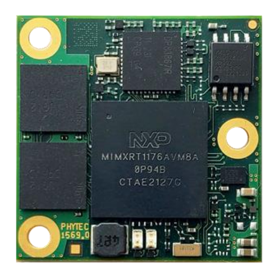
PCM-073/phyCORE-i.MXRT1170 System on Module L-1064e.A0 4.4 Component Placement Diagram Figure 8. phyCORE-i.MXRT1170 Component Placement (processor side) © PHYTEC America L.L.C. 2023... - Page 22 PCM-073/phyCORE-i.MXRT1170 System on Module L-1064e.A0 Figure 9. phyCORE-i.MXRT1170 Component Placement (connector side) A searchable pdf of the phyCORE-I.MXRT1170 component placement can be found here. © PHYTEC America L.L.C. 2023...
-
Page 23: Technical And Electrical Specifications
13.1 Integration. The connectors are not keyed, so it is possible to plug them in backwards. PHYTEC recommends adding mounting holes in your carrier board design to match the ones on the SOM to make the correct orientation more obvious. -
Page 24: Solder Jumpers
Connect VDD_1V8 to switching regulator 0 Ω Connect VDD_1V8 to DCDC_1V8_OUT Connect ADC_VREFH to X_ADC_REF 0 Ω Connect ADC_VREFH to VDDA_ADC_1P8_IN Sets the VDD_EMC2 domain to 3.3V 0 Ω Sets the VDD_EMC2 domain to 1.8V © PHYTEC America L.L.C. 2023... - Page 25 GPIO_AD_00, GPIO_AD_01, GPIO_AD_02, GPIO_AD_03, GPIO_AD_04, GPIO_AD_05, GPIO_AD_06, GPIO_AD_07, GPIO_AD_08, GPIO_AD_09, GPIO_AD_10, GPIO_AD_11, GPIO_AD_12, GPIO_AD_13, GPIO_AD_14, GPIO_AD_15, GPIO_AD_16, GPIO_AD_17, GPIO_AD_18, GPIO_AD_19, GPIO_AD_20, NVCC_GPIO GPIO_AD_21, GPIO_AD_22, GPIO_AD_23, GPIO_AD_24, GPIO_AD_25, GPIO_AD_26, GPIO_AD_27, GPIO_AD_28, GPIO_AD_29, GPIO_AD_30, GPIO_AD_31, GPIO_AD_32, GPIO_AD_33, GPIO_AD_34, GPIO_AD_35 © PHYTEC America L.L.C. 2023...
- Page 26 Overheating the board can cause the solder pads to loosen, rendering the module inoperable. Follow the instructions carefully for whatever method of removal is used. CAUTION: If any modifications to the module are performed, regardless of their nature, the manufacturer warranty is voided. © PHYTEC America L.L.C. 2023...
- Page 27 PCM-073/phyCORE-i.MXRT1170 System on Module L-1064e.A0 Figure 11. Jumper Locations (Processor side) © PHYTEC America L.L.C. 2023...
- Page 28 PCM-073/phyCORE-i.MXRT1170 System on Module L-1064e.A0 Figure 12. Jumper Locations (Connector side) © PHYTEC America L.L.C. 2023...
-
Page 29: Pin Descriptions
Figure 14. The tables also discuss the appropriate voltage domain, signal type, and a description of the functionality. The signal type also includes information about the signal direction. © PHYTEC America L.L.C. 2023... - Page 30 Signal names and descriptions in the following tables 7-10, however, are in regards to the specification of the phyCORE-i.MXRT1170 SOM schematic and may not line up with the functionality defined in PHYTEC’s provided SDK. For information about pin multiplexing contact PHYTEC Support.
-
Page 31: Pinout Table
X_GPIO_SD_B1_00/SD1_CMD 3.3V GPIO_SD_B1_00 SD1 Command X_GPIO_SD_B1_01/SD1_CLK 3.3V GPIO_SD_B1_01 SD1 Clock X_GPIO_SD_B1_02/SD1_D0 3.3V GPIO_SD_B1_02 SD1 Data 0 X_GPIO_SD_B1_03/SD1_D1 3.3V GPIO_SD_B1_03 SD1 Data 1 X_GPIO_SD_B1_04/SD1_D2 3.3V GPIO_SD_B1_04 SD1 Data 2 X_GPIO_SD_B1_05/SD1_D3 3.3V GPIO_SD_B1_05 SD1 Data 3 Ground © PHYTEC America L.L.C. 2023... - Page 32 MIPI DSI Differential Clock (positive) X_MIPI_DSI_CKN Differential MIPI_DSI_CLKN MIPI DSI Differential Clock (negative) X_MIPI_DSI_DP1 Differential MIPI_DSI_DP1 MIPI DSI Differential Data (positive) X_MIPI_DSI_DN1 Differential MIPI_DSI_DN1 MIPI DSI Differential Data (negative) Ground X_MIPI_CSI_DN0 Differential MIPI_CSI_DN0 MIPI CSI Differential Data (negative) © PHYTEC America L.L.C. 2023...
- Page 33 GPIO GPIO X_GPIO_EMC_B2_13 3.3V GPIO_EMC_B2_13 X_GPIO_EMC_B2_15 3.3V GPIO_EMC_B2_15 GPIO Ground GPIO X_GPIO_EMC_B2_18 3.3V GPIO_EMC_B2_18 UART Receive Data X_GPIO_EMC_B1_41/LPUART6_RXD 3.3V GPIO_EMC_B1_41 UART Transmit Data X_GPIO_EMC_B1_40/LPUART6_TXD 3.3V GPIO_EMC_B1_40 GPIO X_GPIO_SNVS_01 1.8V GPIO_SNVS_01 GPIO X_GPIO_SNVS_00 1.8V GPIO_SNVS_00 Ground © PHYTEC America L.L.C. 2023...
- Page 34 Processor Ball Description GPIO X_GPIO_EMC_B2_07 3.3V GPIO_EMC_B2_07 GPIO X_GPIO_EMC_B2_05 3.3V GPIO_EMC_B2_05 GPIO X_GPIO_EMC_B2_03 3.3V GPIO_EMC_B2_03 X_GPIO_EMC_B2_01 3.3V GPIO_EMC_B2_01 GPIO X_GPIO_EMC_B2_08 3.3V GPIO_EMC_B2_08 GPIO Ground X_GPIO_EMC_B2_06 3.3V GPIO_EMC_B2_06 GPIO X_GPIO_EMC_B2_04 3.3V GPIO_EMC_B2_04 GPIO X_GPIO_EMC_B2_02 3.3V GPIO_EMC_B2_02 GPIO © PHYTEC America L.L.C. 2023...
- Page 35 4.7 Solder Jumpers for details This signal should not be driven during reset. More information can be found in section 6.3 System Boot Configuration Do not use this signal if the on-board DDR is populated. © PHYTEC America L.L.C. 2023...
-
Page 36: Layout Guidelines
Surface-mount receptacles are preferred over through-hole connectors, as signals can be routed on the top layer of the PCB without introducing vias to the signal path. If through-hole pins are necessary, it may be beneficial to route signals on the bottom layer. © PHYTEC America L.L.C. 2023... -
Page 37: General Signal Routing Guidelines
Carrier Board provides an easy access current shunt to measure SOM current under various operating conditions as part of your system power analysis. The reference designator of the shunt is R154 and has a value of 8 mΩ (and a size of © PHYTEC America L.L.C. 2023... -
Page 38: Primary Power Reference Circuit
The reference circuits below showcase additional functionality that can be added to the primary power circuit. Figure 16 is a circuit for measuring the input current to the SOM. It contains: • A small resistor (R154) that the current is measured across • A connector to a current measurement board © PHYTEC America L.L.C. 2023... - Page 39 A phoenix connector for connecting a 5V external power source to the system • A fuse/diode circuit (F1/D5) that will trip in case of an overload preventing damage to the rest of the circuit • A transistor network that provides reverse polarity protection © PHYTEC America L.L.C. 2023...
-
Page 40: Backup Power (V_Batt)
SNVS in the processor to maintain time when main system power is removed, the VBAT input must be supplied with power. PHYTEC recommends using either a battery or a large gold cap capacitor (220mF or larger) for powering VBAT. The SNVS draws a maximum of 1 mA and is the only draw on VBAT. For more information regarding the recommended... -
Page 41: Power Sequencing
Prematurely driving the pins may cause current to flow through the I/O pins before the processor is properly powered, potentially resulting in damage or unknown behavior after power-up or reset. Therefore, the peripheral carrier board power should be switched on/enabled by the X_PGOOD signal to avoid powering external peripherals and circuits that © PHYTEC America L.L.C. 2023... -
Page 42: Safe Shutdown And Sudden Power Loss
Another solution is to have a read-only file system as this would ensure nothing is modified in an unexpected manner in the event of an unexpected shutdown. © PHYTEC America L.L.C. 2023... -
Page 43: System Memory
The Q/OSPI Flash can be used for a primary boot and has XIP capability. Contact our sales team for information on the available Q/OSPI population options: https://PHYTEC.com/contact/ © PHYTEC America L.L.C. 2023... -
Page 44: External Memory Bus
Two parallel QSPI memories (FlexSPI1_A, FlexSPI1_B or FlexSPI2_A, FlexSPI2_B) • Two parallel OSPI memories (FlexSPI2_A, FlexSPI2_B) 6.2.1.1 FlexSPI Pinout Table 13 FlexSPI Connections at the phyCORE-Connector Processor X1 Pin #(s) SOM Signal Type Level Description Signal © PHYTEC America L.L.C. 2023... - Page 45 FlexSPI2_A Data 1 X_GPIO_EMC_B2_14 X_GPIO_EMC_B2_15 FLEXSPI2_A_DATA2 3.3V FlexSPI2_A Data 2 X_GPIO_SD_B1_04/SD1_D2 X_GPIO_EMC_B2_16 FLEXSPI2_A_DATA3 3.3V FlexSPI2_A Data 3 X_GPIO_SD_B1_05/SD1_D3 FLEXSPI2_A_DATA4 X_GPIO_EMC_B2_17 3.3V FlexSPI2_A Data 4 FLEXSPI2_A_DATA5 X_GPIO_EMC_B2_18 3.3V FlexSPI2_A Data 5 FLEXSPI2_A_DATA6 3.3V FlexSPI2_A Data 6 X_GPIO_EMC_B2_19/ENET_RGMII_MDC © PHYTEC America L.L.C. 2023...
-
Page 46: Semc
The SEMC module is used internally on the SOM for the SDRAM. 6.2.2.1 SEMC Pinout Table 14 SEMC Connections at the phyCORE-Connector Processor SOM Signal Type Level Description Signal #(s) SEMC_CLKX0 3.3V SEMC Clock 0 X_GPIO_EMC_B2_19/ENET_RGMII_MDC © PHYTEC America L.L.C. 2023... -
Page 47: Usdhc
The i.MXRT1170 processor provides two Secure Digital/MultiMedia Card interfaces USDHC1 and USDHC2. The USDHC ports provides a 4-bit wide data bus that supports embedded MultiMedia Card System Specification, SD Memory Card Specification 3.0, SD Physical Layer Specification v3.0, and SDIO Card specification v3.0. © PHYTEC America L.L.C. 2023... - Page 48 Do not use this signal if the on-board QSPI is populated. 6.2.3.2 USDHC Design In Considerations • USDHC signals should be length matched within 12700 µm as described in Table • Keep USDHC trace lengths as short as possible. © PHYTEC America L.L.C. 2023...
- Page 49 6.2.3.3 USDHC Reference Circuit Two reference circuits using USDHC are shown in the figures below. The first connects the USDHC1 signals to a micro-SD card reader for use as either a data transfer device or a boot device. © PHYTEC America L.L.C. 2023...
- Page 50 Figure 21. SD-Card USDHC1 Reference Schematic The circuit consists of: • An SD-card reader with CMD/DATA line pullups • A load switch The second reference circuit connects USDHC2 to a E key M.2 connector for use in WIFI/BT applications. © PHYTEC America L.L.C. 2023...
-
Page 51: System Boot Configuration
During the power-on reset cycle, the operational system boot mode of the phyCORE-i.MXRT1170 SOM is determined by the configuration of the BOOT_CFG [11:0] and BOOT_MODE_0/1 signals. The BOOT signals must be held at the desired configuration until X_POR_B_OUT goes high to be properly latched into the system. For development and debugging © PHYTEC America L.L.C. 2023... - Page 52 To modify the default boot configuration on a custom carrier board, it is recommended to use 1kΩ pull-up resistors or 10kΩ pull-down resistors to override the SOM settings. For startup/verification testing, PHYTEC recommends designing the boot configuration circuit to include a DIP switch. This will make it easy to swap between various boot modes (an example circuit is shown below).
- Page 53 PCM-073/phyCORE-i.MXRT1170 System on Module L-1064e.A0 Figure 24. Reference Schematic for BOOT configuration © PHYTEC America L.L.C. 2023...
-
Page 54: Serial Interfaces
The voltage level for this signal is configurable for 1.8V or 3.3V. The default voltage level is listed here, but always check the actual jumper setting for the applicable SOM configuration. Refer to section 4.7 Solder Jumpers for details 7.1.2 FlexCAN Reference Circuit An example reference circuit for connecting the CAN3 signals to a 2X5 connector is shown below. © PHYTEC America L.L.C. 2023... -
Page 55: Ethernet
RGMII clock skew. Options such as these can be set via external strapping resistors which are described in the datasheet. The table below lists the default Ethernet PHY strapping configuration; however, these settings can be © PHYTEC America L.L.C. 2023... -
Page 56: Ethernet Pinout
PHY if necessary. Refer to the DP83867IRRGZ datasheet for further details on these configuration and strapping options (DP83867IRRGZ Datasheet). NOTE: Adjusting strapping options and PHY registers is not necessary when using PHYTEC provided SDKs. Table 19 Ethernet PHY Default Strapping Configuration Strapping Option Default Setting Strapping Signals... - Page 57 ENET_1G_COL X_GPIO_EMC_B2_10 3.3V ENET_1G Collision Detect ENET_1G_CRS X_GPIO_EMC_B2_09 3.3V ENET_1G Carrier Sense X_GPIO_EMC_B2_20/ENET_RGMII_MDIO pulldown on SOM) ENET_1G Management Data X_GPIO_EMC_B1_41/LPUART6_RXD ENET_1G_MDIO 3.3V X_GPIO_AD_17/SAI1_MCLK X_GPIO_AD_33/ENET_MDIO X_GPIO_EMC_B2_19/ENET_RGMII_MDC ENET_1G Management Data pulldown on SOM) ENET_1G_MDC 3.3V Clock X_GPIO_EMC_B1_40/LPUART6_TXD © PHYTEC America L.L.C. 2023...
- Page 58 (10K pulldown on SOM) ENET_1G_TX_DATA3 3.3V ENET_1G Transmit Data 3 X_GPIO_EMC_B2_03 X_GPIO_SD_B2_11 X_GPIO_DISP_B1_11/BT_CFG05 (10K pulldown on ENET_1G_TX_CLK 3.3V ENET_1G Transmit Clock SOM) X_GPIO_EMC_B2_14 X_GPIO_DISP_B1_10/BT_CFG04 (10K pulldown on SOM) ENET_1G_TX_EN 3.3V ENET_1G Transmit Enable X_GPIO_EMC_B2_13 X_GPIO_SD_B2_10 © PHYTEC America L.L.C. 2023...
- Page 59 ENET_QOS Transmit Data 0 X_GPIO_DISP_B2_02/ENET_TX_DATA0/BT_CFG_08 (10K pulldown on SOM) X_GPIO_DISP_B1_08/BT_CFG02 (10K pulldown on SOM) ENET_QOS_TX_DATA1 3.3V ENET_QOS Transmit Data 1 X_GPIO_DISP_B2_03/ENET_TX_DATA1/BT_CFG_09 (10K pulldown on SOM) X_GPIO_DISP_B1_07/BT_CFG01 (10K pulldown on ENET_QOS_TX_DATA2 3.3V ENET_QOS Transmit Data 2 SOM) © PHYTEC America L.L.C. 2023...
-
Page 60: Ethernet Design In Guide
(µm) Trace Trace X_ETH_A_P 3772 101600 92828 X_ETH_A_N 3700 101600 97900 X_ETH_B_P 3112 101600 98488 X_ETH_B_N 3037 101600 98563 X_ETH_C_P 3119 101600 98481 X_ETH_C_N 3162 101600 98438 X_ETH_D_P 3353 101600 98247 X_ETH_D_N 3438 101600 98162 © PHYTEC America L.L.C. 2023... - Page 61 6.5ps/mm. However, the actual physical trace delay will vary depending on the PCB stackup, materials, etc. • Transmit Clock Length Calculation with Physical Trace Delay: (X µm) + (Average total length of control/data signals on Carrier Board) + (276860 µm) – (Xµm) © PHYTEC America L.L.C. 2023...
-
Page 62: Ethernet Reference Circuits
ENET_1G_RX_DATA3 24488 120000 95512 7.2.3 Ethernet Reference Circuits Example reference circuits for connecting the ETH0 differential signals from the on-board PHY to an RJ45 connector and ENET1 signals to an Ethernet PHY are shown below. © PHYTEC America L.L.C. 2023... - Page 63 PCM-073/phyCORE-i.MXRT1170 System on Module L-1064e.A0 Figure 26. RJ45 Reference Schematic The circuit consists of: • An Ethernet Jack • Two TVS diode arrays for ESD protection • Two resistors to manage the Ethernet LEDs in the jack © PHYTEC America L.L.C. 2023...
-
Page 64: Flexio
Emulation of numerous serial/parallel communication protocols including: o UART o I2C o SPI o I2S o Camera IF o Motorala 68K/Interl 8080 bus o PWM o Input-capture • Flexible 16-bit timers with support for various trigger, reset, enable and disable conditions © PHYTEC America L.L.C. 2023... -
Page 65: Flexio Pinout
The voltage level for this signal is configurable for 1.8V or 3.3V. The default voltage level is listed here, but always check the actual jumper setting for the applicable SOM configuration. Refer to section 4.7 Solder Jumpers for details © PHYTEC America L.L.C. 2023... -
Page 66: Lpic
Aside from LPI2C2, which has pullups on the SOM, all the I C signals require pullups in your custom CB design. CAUTION: LPI2C2 is used by the EEPROM (I C address 0x50). Ensure any external use of the LPI2C2 line does not interfere with this communication. © PHYTEC America L.L.C. 2023... -
Page 67: Lpic Pinout
Do not use this signal if the on-board DDR is populated. 7.5 LPSPI The Serial Peripheral Interface (SPI) is a transmit/receive, master/slave synchronous serial bus. The phyCORE- i.MXRT1170 SOM provides access to four SPI ports at the phyCORE-Connector. © PHYTEC America L.L.C. 2023... -
Page 68: Lpspi Pinout
LPSPI3 Data Out X_GPIO_DISP_B1_06/BT_CFG00 (10K pulldown on SOM) X_GPIO_EMC_B2_07 LPSPI3_SIN 3.3V LPSPI3 Data In X_GPIO_DISP_B1_05 X_GPIO_SD_B2_00 LPSPI4_SCK 3.3V LPSPI4 Clock X_GPIO_DISP_B2_12/LPUART2_CTS_B X_GPIO_SD_B2_01 LPSPI4_PCS0 3.3V LPSPI4 Chip Select 0 X_GPIO_DISP_B2_15/GPIO5_16 LPSPI4_PCS1 X_GPIO_SD_B2_04 3.3V LPSPI4 Chip Select 1 © PHYTEC America L.L.C. 2023... -
Page 69: Lpuart
LPUART1 is the default console in many example programs and as such PHYTEC recommends bringing out LPUART1 for console access. More information on using it as a debug console is provided in section 11.3... - Page 70 UART9 Receive Data LPUART9_TXD X_GPIO_SD_B2_00 3.3V UART9 Transmit Data LPUART10_CTS_B X_GPIO_AD_34/SD1_VSELECT 3.3V UART10 Clear to Send LPUART10_RTS_B X_GPIO_AD_35/SD1_RESET_B 3.3V UART10 Request to Send X_GPIO_AD_16 LPUART10_RXD 3.3V UART10 Receive Data X_GPIO_AD_33/ENET_MDIO X_GPIO_AD_15 LPUART10_TXD 3.3V UART10 Transmit Data X_GPIO_AD_32/ENET_MDC © PHYTEC America L.L.C. 2023...
- Page 71 6.3 System Boot Configuration Do not use this signal if the on-board ethernet PHY is populated. Do not use this signal if the on-board DDR is populated. Do not use this signal if the on-board QSPI is populated. © PHYTEC America L.L.C. 2023...
-
Page 72: Usb
Table 30 phyCORE-I.MXRT1170 USB0 Layout Characteristics Signal Name Length (µm) Length Single Ended Differential Matching Impedance (Ω) Impedance (Ω) Max Total Max CB (µm) Trace Trace X_USB_OTG1_DP 17493 304800 287307 1270 X_USB_OTG1_DN 17175 304800 287625 © PHYTEC America L.L.C. 2023... -
Page 73: Usb Reference Circuits
AC97 • • Codec/DSP 7.8.1 SAI Pinout Table 31 SAI Connections at the phyCORE-Connector Processor Signal X1 Pin #(s) SOM Signal(s) Type Level Description X_GPIO_AD_17/SAI1_MCLK SAI1_MCLK 3.3V SAI1 M Clock X_GPIO_DISP_B2_03/ENET_TX_DATA1/BT_CFG_09 (10K pulldown on SOM) © PHYTEC America L.L.C. 2023... - Page 74 SAI4 M Clock X_GPIO_LPSR_00/CAN3_TX X_GPIO_LPSR_07/LPSPI5_PCS2 SAI4_RX_BCLK 3.3V SAI4 Receive Bit Clock X_GPIO_LPSR_14/JTAG_TCK X_GPIO_LPSR_06/LPSPI5_PCS1 SAI4_RX_DATA 3.3V SAI4 Receive Data X_GPIO_LPSR_13/JTAG_MOD X_GPIO_LPSR_08/LPI2C5_SDA SAI4_RX_SYNC 3.3V SAI4 Receive Frame Sync X_GPIO_LPSR_15/JTAG_TMS X_GPIO_LPSR_04/LPSPI5_SDO SAI4_TX_BCLK 3.3V SAI4 Transmit Bit Clock X_GPIO_LPSR_12/JTAG_TDI © PHYTEC America L.L.C. 2023...
-
Page 75: Spdif
The following sub-sections detail each of the display/camera interfaces supported on the phyCORE-i.MXRT1170. 8.1 VIDEO MUX The phyCORE-I.MXRT1170 SOM video mux provides mux control for the following interfaces: • Parallel CSI (IO PADs) • MIPI CSI-2 • MIPI DSI © PHYTEC America L.L.C. 2023... -
Page 76: Video Mux Pinout
VIDEO_MUX_LCDIF_DATA14 X_GPIO_DISP_B2_06/ENET_RX_DATA0 3.3V LCDIF Data VIDEO_MUX_LCDIF_DATA15 X_GPIO_DISP_B2_07/ENET_RX_DATA1 3.3V LCDIF Data VIDEO_MUX_LCDIF_DATA16 X_GPIO_DISP_B2_08/ENET_RX_EN 3.3V LCDIF Data VIDEO_MUX_LCDIF_DATA17 X_GPIO_DISP_B2_09/ENET_RX_ER 3.3V LCDIF Data VIDEO_MUX_LCDIF_DATA18 X_GPIO_DISP_B2_10/LPUART2_TXD 3.3V LCDIF Data VIDEO_MUX_LCDIF_DATA19 X_GPIO_DISP_B2_11/LPUART2_RXD 3.3V LCDIF Data VIDEO_MUX_LCDIF_DATA20 X_GPIO_DISP_B2_12/LPUART2_CTS_B 3.3V LCDIF Data © PHYTEC America L.L.C. 2023... -
Page 77: Mipi-Dsi
The phyCORE-i.MXRT1170 SOM brings out a MIPI-DSI display port with two data lanes and one clock lane to support 16, 18 and 24 bit pixel data and all alignment configurations. More information about the supported video formats are discussed in the i.MXRT1170 Technical Reference Manual. © PHYTEC America L.L.C. 2023... -
Page 78: Mipi-Dsi Pinout
11298 MIPI-DSI MIPI_DSI_DP0 11365 MIPI_DSI_DN1 10994 MIPI_DSI_DP1 10959 MIPI_DSI_CLKN 11077 MIPI_DSI_CLKP 11145 8.2.3 MIPI-DSI Reference Circuits Example reference circuits for connecting the MIPI-DSI, I2C, and backlight control signals to a 40-pin connector are shown below. © PHYTEC America L.L.C. 2023... -
Page 79: Mipi-Csi
The phyCORE-i.MXRT1170 SOM brings out one 4 lane CSI (camera serial interface). The CSI interfaces provide the following functionality: • Support for all CSI-2 data types • Support for 1 or 2 data lane mode up to 1.5Gbps per lane © PHYTEC America L.L.C. 2023... -
Page 80: Mipi-Csi Pinout
8.3.3 MIPI-CSI Reference Circuits Example reference circuits for connecting the MIPI-CSI signals to a 30-pin connector are shown below. The 30-pin connector pinout is designed to connect to a PHYTEC camera and supports both 3.3V and 5V cameras. © PHYTEC America L.L.C. 2023... - Page 81 PCM-073/phyCORE-i.MXRT1170 System on Module L-1064e.A0 Figure 31. MIPI-CSI Power Toggle Reference Schematic © PHYTEC America L.L.C. 2023...
-
Page 82: Control Interfaces
The following sub-sections detail each of the control interfaces supported on the phyCORE-i.MXRT1170. 9.1 Clock Control Module The phyCORE-i.MXRT1170 SOM contains a Clock Control Module (CCM) that manages the on-chip module clocks and will generate clock sources with fixed or variable frequencies. © PHYTEC America L.L.C. 2023... -
Page 83: Ccm Pinout
X_GPIO_AD_28/LPUART5_TXD 3.3V FlexPWM2 Output 2A FLEXPWM2_PWM0_B X_GPIO_AD_25/LPUART1_RXD 3.3V FlexPWM2 Output 0B FLEXPWM2_PWM1_B X_GPIO_AD_27 3.3V FlexPWM2 Output 1B FLEXPWM2_PWM2_B X_GPIO_AD_29/LPUART5_RXD 3.3V FlexPWM2 Output 2B FLEXPWM2_PWM0_X X_GPIO_AD_10/USB_OTG1_PWR 3.3V FlexPWM2 Output 0X FLEXPWM2_PWM1_X X_GPIO_AD_11/USB_OTG1_OC 3.3V FlexPWM2 Output 1X © PHYTEC America L.L.C. 2023... -
Page 84: Power Gating And Memory Controller
SOM configuration. Refer to section 4.7 Solder Jumpers for details 10 Peripheral Interfaces The following sub-sections detail each of the peripheral interfaces supported on the phyCORE-i-.MXRT1170. 10.1 ACMP The phyCORE-i.MXRT1170 SOM brings out four analog comparator modules. © PHYTEC America L.L.C. 2023... -
Page 85: Acmp Pinout
X_GPIO_AD_09/USB_OTG1_ID 3.3V ADC1 Channel 1B ADC1_CH2A X_GPIO_AD_10/USB_OTG1_PWR 3.3V ADC1 Channel 2A ADC1_CH2B X_GPIO_AD_11/USB_OTG1_OC 3.3V ADC1 Channel 2B ADC1_CH3A X_GPIO_AD_12 3.3V ADC1 Channel 3A ADC1_CH3B X_GPIO_AD_13 3.3V ADC1 Channel 3B ADC1_CH4A X_GPIO_AD_14/GPIO9_13 3.3V ADC1 Channel 4A © PHYTEC America L.L.C. 2023... -
Page 86: Emvsim
EMVSIM1_RST 3.3V EMVSIM Reset X_GPIO_EMC_B2_13 X_GPIO_AD_03/LPUART8_RXD EMVSIM1_SVEN 3.3V EMVSIM Power Enable X_GPIO_EMC_B2_14 X_GPIO_AD_00/GPIO8_31 EMVSIM1_IO 3.3V EMVSIM Data X_GPIO_EMC_B2_11 X_GPIO_DISP_B2_11/LPUART2_RXD EMVSIM2_CLK 3.3V EMVSIM Clock X_GPIO_AD_07/USB_OTG2_PWR X_GPIO_DISP_B2_14 (10K pullup on EMVSIM2_PD 3.3V EMVSIM Card Presence Detect SOM) © PHYTEC America L.L.C. 2023... -
Page 87: Gpio
227 GPIOs available depending on the multiplexing configuration. Note that not all GPIOs can be used simultaneously as there is overlap of connector pins between the GPIO modules. Table 44 Total Available GPIO Number of GPIO Available GPIO Module GPIO_MUX2 GPIO_MUX3 GPIO4 GPIO5 GPIO6 © PHYTEC America L.L.C. 2023... -
Page 88: Gpio Pinout
The voltage level for this signal is configurable for 1.8V or 3.3V. The default voltage level is listed here, but always check the actual jumper setting for the applicable SOM configuration. Refer to section 4.7 Solder Jumpers for details Do not use this signal if the on-board ethernet PHY is populated. Do not use this signal if the on-board DDR is populated. © PHYTEC America L.L.C. 2023... - Page 89 X1 Pin #(s) SOM Signal(s) Type Level Internal SOM Usage Signal GPIO4_IO00 X_GPIO_AD_33/ENET_MDIO 3.3V None GPIO4_IO01 X_GPIO_AD_34/SD1_VSELECT 3.3V None GPIO4_IO02 X_GPIO_AD_35/SD1_RESET_B 3.3V None GPIO4_IO03 X_GPIO_SD_B1_00/SD1_CMD 3.3V None GPIO4_IO04 X_GPIO_SD_B1_01/SD1_CLK 3.3V None GPIO4_IO05 X_GPIO_SD_B1_02/SD1_D0 3.3V None © PHYTEC America L.L.C. 2023...
- Page 90 10K pulldown on SOM GPIO5_IO07 X_GPIO_DISP_B2_06/ENET_RX_DATA0 3.3V None GPIO5_IO08 X_GPIO_DISP_B2_07/ENET_RX_DATA1 3.3V None GPIO5_IO09 X_GPIO_DISP_B2_08/ENET_RX_EN 3.3V None GPIO5_IO10 X_GPIO_DISP_B2_09/ENET_RX_ER 3.3V None GPIO5_IO11 X_GPIO_DISP_B2_10/LPUART2_TXD 3.3V None GPIO5_IO12 X_GPIO_DISP_B2_11/LPUART2_RXD 3.3V None GPIO5_IO13 X_GPIO_DISP_B2_12/LPUART2_CTS_B 3.3V None GPIO5_IO14 X_GPIO_DISP_B2_13/LPUART2_RTS_B 3.3V None © PHYTEC America L.L.C. 2023...
- Page 91 X_GPIO_EMC_B2_01 3.3V None GPIO8_IO12 X_GPIO_EMC_B2_02 3.3V None GPIO8_IO13 X_GPIO_EMC_B2_03 3.3V None GPIO8_IO14 X_GPIO_EMC_B2_04 3.3V None GPIO8_IO15 X_GPIO_EMC_B2_05 3.3V None GPIO8_IO16 X_GPIO_EMC_B2_06 3.3V None GPIO8_IO17 X_GPIO_EMC_B2_07 3.3V None GPIO8_IO18 X_GPIO_EMC_B2_08 3.3V None GPIO8_IO19 X_GPIO_EMC_B2_09 3.3V None © PHYTEC America L.L.C. 2023...
- Page 92 4.7K pullup on SOM GPIO9_IO18 X_GPIO_AD_19/LPI2C2_SDA 3.3V 4.7K pullup on SOM GPIO9_IO19 X_GPIO_AD_20/SAI1_RX_DATA0 3.3V None GPIO9_IO20 X_GPIO_AD_21/SAI1_TX_DATA0 3.3V None GPIO9_IO21 X_GPIO_AD_22/SAI1_TX_BCLK 3.3V None GPIO9_IO22 X_GPIO_AD_23/SAI1_TX_SYNC 3.3V None GPIO9_IO23 X_GPIO_AD_24/LPUART1_TXD 3.3V None GPIO9_IO24 X_GPIO_AD_25/LPUART1_RXD 3.3V None © PHYTEC America L.L.C. 2023...
- Page 93 This signal should not be driven during reset. More information can be found in section 6.3 System Boot Configuration Do not use this signal if the on-board ethernet PHY is populated. Do not use this signal if the on-board QSPI is populated. © PHYTEC America L.L.C. 2023...
- Page 94 The voltage level for this signal is configurable for 1.8V or 3.3V. The default voltage level is listed here, but always check the actual jumper setting for the applicable SOM configuration. Refer to section 4.7 Solder Jumpers for details This signal should not be driven during reset. More information can be found in section 6.3 System Boot Configuration © PHYTEC America L.L.C. 2023...
-
Page 95: Gpt
GPT2 Clock GPT2_COMPARE1 X_GPIO_AD_02/LPUART8_TXD 3.3V GPT2 Compare GPT2_COMPARE2 X_GPIO_AD_03/LPUART8_RXD 3.3V GPT2 Compare GPT2_COMPARE3 X_GPIO_AD_04/LPUART8_CTS_B 3.3V GPT2 Compare X_GPIO_EMC_B2_06 GPT3_CAPTURE1 3.3V GPT3 Capture X_GPIO_AD_06/USB_OTG2_OC X_GPIO_EMC_B2_07 GPT3_CAPTURE2 3.3V GPT3 Capture X_GPIO_AD_07/USB_OTG2_PWR X_GPIO_EMC_B2_05 GPT3_CLK 3.3V GPT3 Clock X_GPIO_AD_11/USB_OTG1_OC © PHYTEC America L.L.C. 2023... -
Page 96: Kpp
3.3V KPP Row 2 KPP_ROW3 X_GPIO_AD_28/LPUART5_TXD 3.3V KPP Row 3 KPP_ROW4 X_GPIO_AD_26 3.3V KPP Row 4 KPP_ROW5 X_GPIO_AD_24/LPUART1_TXD 3.3V KPP Row 5 X_GPIO_AD_22/SAI1_TX_BCLK KPP_ROW6 3.3V KPP Row 6 X_GPIO_SD_B1_02/SD1_D0 KPP_ROW7 X_GPIO_AD_20/SAI1_RX_DATA0 3.3V KPP Row 7 © PHYTEC America L.L.C. 2023... -
Page 97: Mqs
SOM Signal(s) Type Level Description X_GPIO_LPSR_01/CAN3_RX PDM_DATA0 3.3V PDM Data X_GPIO_LPSR_09/LPI2C5_SCL X_GPIO_LPSR_13/JTAG_MOD PDM_DATA1 3.3V PDM Data X_GPIO_LPSR_10/JTAG_NTRST X_GPIO_LPSR_14/JTAG_TCK PDM_DATA2 3.3V PDM Data X_GPIO_LPSR_11/JTAG_TDO X_GPIO_LPSR_15/JTAG_TMS PDM_DATA3 3.3V PDM Data X_GPIO_LPSR_12/JTAG_TDI X_GPIO_LPSR_00/CAN3_TX PDM_CLK 3.3V PDM Clock X_GPIO_LPSR_08/LPI2C5_SDA © PHYTEC America L.L.C. 2023... -
Page 98: Pit
The phyCORE-I.MXRT1170 SOM brings out 4x Quad Timer modules. Each 16-bit counter/timer module contains a prescaler, a counter, a load register, a hold register, acapture register, two compare registers, two status and control registers, and one control register. All of these registers are read/writable except the prescaler. © PHYTEC America L.L.C. 2023... -
Page 99: Quad Timer Pinout
This signal should not be driven during reset. More information can be found in section 6.3 System Boot Configuration Do not use this signal if the on-board ethernet PHY is populated. Do not use this signal if the on-board DDR is populated. © PHYTEC America L.L.C. 2023... -
Page 100: Wdog
Processor Signal X1 Pin #(s) SOM Signal(s) Type Level Description XBAR_INOUT12 X_GPIO_EMC_B1_40/LPUART6_TXD 3.3V XBAR Input/Output XBAR_INOUT13 X_GPIO_EMC_B1_41/LPUART6_RXD 3.3V XBAR Input/Output XBAR_INOUT14 X_GPIO_EMC_B2_16 3.3V XBAR Input/Output XBAR_INOUT15 X_GPIO_EMC_B2_17 3.3V XBAR Input/Output XBAR_INOUT16 X_GPIO_EMC_B2_18 3.3V XBAR Input/Output © PHYTEC America L.L.C. 2023... - Page 101 6.3 System Boot Configuration Do not use this signal if the on-board ethernet PHY is populated. Do not use this signal if the on-board DDR is populated. Do not use this signal if the on-board QSPI is populated. © PHYTEC America L.L.C. 2023...
-
Page 102: Debug Interfaces
SOM configuration. Refer to section 4.7 Solder Jumpers for details 11.1.2 JTAG Reference Circuit An example reference circuit for connecting the JTAG signals to a 2x5 connector is shown below. Figure 33. JTAG Reference Schematic © PHYTEC America L.L.C. 2023... -
Page 103: Arm Debug And Trace
The phyCORE-i.MXRT1170 SOM can also be communicated with using LPUART1 for downloading program code into the internal RAM or for debugging programs currently executing. LPUART1 is the default console in many example programs and as such PHYTEC recommends bringing out LPUART1 for console access. The LPUART1 interface is accessible via the phyCORE-Connector. -
Page 104: Lpuart1 Reference Circuits
A dual UART to USB bridge to convert the UART signals into USB signals • A TVS diode array for ESD protection • A micro-USB connector A simpler design that just brings out the bare minimum UART signals for use with FTDI USB adapter cables is shown below. © PHYTEC America L.L.C. 2023... - Page 105 PCM-073/phyCORE-i.MXRT1170 System on Module L-1064e.A0 Figure 35. Simple LPUART1 Reference Schematic © PHYTEC America L.L.C. 2023...
-
Page 106: System Interfaces
The voltage level for this signal is configurable for 1.8V or 3.3V. The default voltage level is listed here, but always check the actual jumper setting for the applicable SOM configuration. Refer to section 4.7 Solder Jumpers for details. © PHYTEC America L.L.C. 2023... -
Page 107: Heartbeat Leds
The phyCORE-i.MXRT1170 has two LEDs, one green and one red, named the heartbeat LEDs. The user can configure the LEDs to behave in a manner most suitable to their design needs, but PHYTEC recommends using them as a visual indicator that the board is booting during debug. The red LED is connected to GPIO_SNVS_08 (processor ball N9) and the green LED is connected to GPIO_SNVS_09 (processor ball R11). -
Page 108: Integrating And Updating The Phycore-I.mxrt1170
13.3 In-Field Updates It is important that your system is designed so that firmware can be updated remotely in case there are issues "in the field." PHYTEC recommends choosing at least one or more of the following design features: •... -
Page 109: Product Change Management
13.4 Product Change Management Use of PHYTEC products ensures interchangeable SoC core circuitry in the event of obsolescence of parts used on our SOMs and SBCs. End users no longer need to redesign entire CPU circuitry and engage in version control to accommodate new or obsolete parts. -
Page 110: Additional Information
PHYTEC System on Modules (SOM) and Single Board Computers (SBC) are designed as subcomponents for integration in electrical devices. Combined with PHYTEC Carrier Boards, PHYTEC SOMs can be used as dedicated Evaluation Boards (i.e.: for use as a test and prototype platform for hardware/software development) in laboratory environments. - Page 111 Additionally, PHYTEC offers no guarantee nor accepts any liability for damages arising from the improper usage or improper installation of the hardware or software. PHYTEC further reserves the right to alter the layout and/or design of the hardware without prior notification and accepts no liability for doing so.
-
Page 112: Revision History
PCM-073/phyCORE-i.MXRT1170 System on Module L-1064e.A0 15 Revision History Table 70 Document Revision History Date Version Number Changes in this Manual 12/21/2023 Preliminary Release © PHYTEC America L.L.C. 2023...
Need help?
Do you have a question about the phyCORE-i.MX RT1170 and is the answer not in the manual?
Questions and answers