
Related Manuals for Phytec L-1009e.A2 phyCORE-i.MX 8M Plus


Summary of Contents for Phytec L-1009e.A2 phyCORE-i.MX 8M Plus
- Page 1 L-1009e.A2 phyCORE-i.MX 8M Plus/phyBOARD- Pollux (1549.2/1552.2) Hardware Manual A product of PHYTEC Technology Holding Company...
- Page 2 L-1009e.A2 phyCORE-i.MX 8M Plus/phyBOARD-Pollux (1549.2/1552.2) Hardware Manual L-1009e.A2 phyCORE-i.MX 8M Plus/phyBOARD-Pollux (1549.2/1552.2) Hardware Manual Document Title L-1009e.A2 phyCORE-i.MX 8M Plus/phyBOARD-Pollux (1549.2/1552.2) Hardware Manual Article Number L-1009e.A2 Release Date 24.06.2022 SOM Prod. No. PCM-070 / PCL-070 (DSC) SOM PCB No. 1549.2 / 1561.0 (DSC)
- Page 3 L-1009e.A2 phyCORE-i.MX 8M Plus/phyBOARD-Pollux (1549.2/1552.2) Hardware Manual © PHYTEC Messtecknik GmbH...
- Page 4 The schematics shown in this hardware manual are believed to be correct. However, correctness can not be guaranteed. The schematics have been pulled from PHYTEC's designs that have been built, tested, and is known to work. The schematics have been re-formatted to fit better in this hardware manual.
- Page 5 Manual 2 Preface As a member of PHYTEC's phyCORE® product family, the phyCORE‑i.MX 8M Plus is one of a series of PHYTEC System on Modules (SOMs) that can be populated with different controllers, various types of memory (RAM, NAND flash, eMMC), and many other features.
- Page 6 Populated on the SOM / SBC With the purchase of a PHYTEC SOM / SBC, you will, in addition to our hardware and software possibilities, receive free obsolescence maintenance service for the hardware we provide. Our PCM (Product Change Management) team of developers is continuously processing all incoming PCN's (Product Change Notifications) from vendors and distributors concerning parts that are used in our products. Possible impacts on the functionality of our products...
- Page 7 2.5 PHYTEC Documentation PHYTEC will provide a variety of hardware and software documentation for all of our products. This includes any or all of the following: •...
- Page 8 L-1009e.A2 phyCORE-i.MX 8M Plus/phyBOARD-Pollux (1549.2/1552.2) Hardware Manual After finishing the Quickstart Guide, we recommend working through the Development Environment Guide. This will give you a comprehensive overview of the features and functions of both the SOM and carrier board.
- Page 9 L-1009e.A2 phyCORE-i.MX 8M Plus/phyBOARD-Pollux (1549.2/1552.2) Hardware Manual 3 Conversions, Abbreviations, and Acronyms Due to part maintenance for our products (which are subject to continuous changes), we refrain from providing detailed, part-specific information within this manual. Please read the section Product Change Management and Information Regarding Parts Populated on the SOM / SBC within the...
- Page 10 L-1009e.A2 phyCORE-i.MX 8M Plus/phyBOARD-Pollux (1549.2/1552.2) Hardware Manual 3.2 Types of Signals Different types of signals are brought out at the phyCORE-Connector. The following table lists the abbreviations used to specify the type of signal. TABLE 1: Signal Types Signal Type...
- Page 11 L-1009e.A2 phyCORE-i.MX 8M Plus/phyBOARD-Pollux (1549.2/1552.2) Hardware Manual Signal Type Description Abbreviation PCIe IO Differential line pairs 100 Ohm PCIe level input or output PCIe_I/O HDMI Input Differential line pairs 100 Ohm HDMI level input HDMI_I HDMI Output Differential line pairs 100 Ohm HDMI level output HDMI_O MIPI CSI-2 Input ...
- Page 12 L-1009e.A2 phyCORE-i.MX 8M Plus/phyBOARD-Pollux (1549.2/1552.2) Hardware Manual 3.3 Abbreviations and Acronyms Many acronyms and abbreviations are used throughout this manual. Use the following table to navigate unfamiliar terms used in this document. TABLE 2: Abbreviations and Acronyms Used in this Manual...
- Page 13 L-1009e.A2 phyCORE-i.MX 8M Plus/phyBOARD-Pollux (1549.2/1552.2) Hardware Manual Abbreviation Definition Single Board Computer Surface mount technology ® System on Module; used in reference to the PCM-070 /phyCORE -i.MX 8M Plus module User button Sx (e.g. S1, S2, etc.) used in reference to the available user buttons, or DIP-...
- Page 14 Manual phyCORE-i.MX 8M Plus Introduction The phyCORE‑i.MX 8M Plus belongs to PHYTEC’s phyCORE System on Module family. The phyCORE SOMs represent the continuous development of the PHYTEC System on Module technology. Like its mini-, micro-, and nanoMODUL predecessors, phyCORE boards integrate all core elements of a microcontroller system on a subminiature board and are designed in a manner that ensures their easy expansion and embedding in peripheral hardware developments.
- Page 15 All processor interfaces available at the SOM Connector • Available for different temperature grades (see Product Temperature Grades) The maximum memory size listed as of the printing of this manual. Please contact PHYTEC for more information about additional or new module configurations available. © PHYTEC Messtecknik GmbH...
- Page 16 L-1009e.A2 phyCORE-i.MX 8M Plus/phyBOARD-Pollux (1549.2/1552.2) Hardware Manual 4.2 phyCORE-i.MX 8M Plus Block Diagram FIGURE 1: phyCORE-i.MX 8M Plus Block Diagram © PHYTEC Messtecknik GmbH...
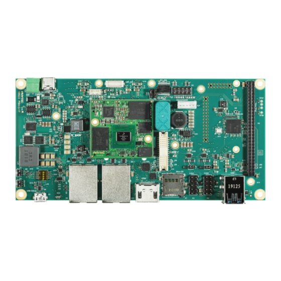
- Page 17 L-1009e.A2 phyCORE-i.MX 8M Plus/phyBOARD-Pollux (1549.2/1552.2) Hardware Manual 4.3 phyCORE-i.MX 8M Plus Component Placement FIGURE 2: phyCORE-i.MX 8M Plus Component Placement (Top View) © PHYTEC Messtecknik GmbH...
- Page 18 L-1009e.A2 phyCORE-i.MX 8M Plus/phyBOARD-Pollux (1549.2/1552.2) Hardware Manual FIGURE 3: phyCORE-i.MX 8M Plus Component Placement (Bottom View) FIGURE 4: phyCORE-i.MX 8M Plus DSC Component Placement (Top View) © PHYTEC Messtecknik GmbH...
- Page 19 L-1009e.A2 phyCORE-i.MX 8M Plus/phyBOARD-Pollux (1549.2/1552.2) Hardware Manual FIGURE 5: phyCORE-i.MX 8M Plus DSC Component Placement (Bottom View) © PHYTEC Messtecknik GmbH...
- Page 20 L-1009e.A2 phyCORE-i.MX 8M Plus/phyBOARD-Pollux (1549.2/1552.2) Hardware Manual phyCORE-i.MX 8M Plus Minimum Operating Requirements Warning We recommend connecting all available +3.3 V input pins to the power supply system on a custom carrier board housing the phyCORE-i.MX 8M Plus and, at minimum, the matching number of GND balls neighboring the +3.3 V balls.
- Page 21 Logic) must be used. Pin Muxing Warning If pin settings are changed from the PHYTEC standard configuration, make sure that the setting of the pull resistors are adjusted accordingly. Never rely on the SoC-internal pull resistor. © PHYTEC Messtecknik GmbH...
- Page 22 Warning Due to the small footprint of the solder jumpers (J), PHYTEC does not recommend manual jumper modifications. This may also render the warranty invalid. Contact our sales team if you need jumper configurations different from the default configuration.
- Page 23 L-1009e.A2 phyCORE-i.MX 8M Plus/phyBOARD-Pollux (1549.2/1552.2) Hardware Manual The jumpers (J = solder jumper) have the following functions. TABLE 3: Jumper Settings Jumper Position Description Type Section 1+2 (default) RTC_CLKOUT is connected to 0201 X_RTC_CLKOUT/nTEMP_ALERT nTEMP_ALERT is connected to Temperature Sensors X_RTC_CLKOUT/nTEMP_ALERT ...
- Page 24 Warning As a general design rule, PHYTEC recommends connecting all GND pins to neighboring signals which are being used in the application circuitry. For maximum EMI performance, all GND pins should be connected to a solid ground plane. Additionally take care of a solid, low impedance connection of the power supply line to avoid voltage drop.
- Page 25 L-1009e.A2 phyCORE-i.MX 8M Plus/phyBOARD-Pollux (1549.2/1552.2) Hardware Manual External Logic IO Supply Voltage The voltage level (VDD_IO) of the phyCORE’s logic interface circuitry is VDD_3V3 (3.3 V) or VDD_1V8 (1.8 V) which is determined by the configuration input signal X_VIO_Ctrl (X1-D8). Connect X_VIO_Ctrl to the module input supply voltage VIN_3V3 to configure VDD_IO=3.3 V interface voltage level or connect it to GND to select VDD_IO=1.8 V...
- Page 26 L-1009e.A2 phyCORE-i.MX 8M Plus/phyBOARD-Pollux (1549.2/1552.2) Hardware Manual Reset The X_PMIC_RST_B signal (Pin X1-C11) on the phyCORE-Connector is designated as a "cold reset" input. Driving X_PMIC_RST_B to low (has weak pull-up to SNVS_1V8) will restart the system performing a complete power recycle.
- Page 27 L-1009e.A2 phyCORE-i.MX 8M Plus/phyBOARD-Pollux (1549.2/1552.2) Hardware Manual System Boot Configuration Most features of the i.MX 8 Plus microcontroller are configured and/or programmed during the initialization routine. Other features, which impact program execution, must be configured prior to initialization via pin termination.
- Page 28 L-1009e.A2 phyCORE-i.MX 8M Plus/phyBOARD-Pollux (1549.2/1552.2) Hardware Manual configuration on the module or by connecting configuration resistors (e.g. 4,7 kΩ pull-up) to the X_BOOT_MODE configuration signals. The pull-up resistors must be supplied by the right VDD_IO voltage level of 1.8 V or 3.3 V...
- Page 29 L-1009e.A2 phyCORE-i.MX 8M Plus/phyBOARD-Pollux (1549.2/1552.2) Hardware Manual Warning Modules up to revision PCM-070-0F3243I.A1, PCM-070-0F3243I.S1, PCM-070-0F5443I.A0 PCL-070-0F3243I.A0 are configured for boot from internal fuses. These modules have a populated 100 kΩ pull-down resistor R88 and the 4,7 kΩ pull-up resistor R45 is unpopulated.
- Page 30 The three lower address bits are fixed to 0x1 which means that the EEPROM can be accessed at I C address 0x51. The EEPROM has a second address on 0x59, which is called Identification Page, and is reserved for internal PHYTEC uses only.
- Page 31 L-1009e.A2 phyCORE-i.MX 8M Plus/phyBOARD-Pollux (1549.2/1552.2) Hardware Manual 10.4 QSPI NOR Flash (U5) The QSPI NOR Flash memory of the phyCORE-i.MX 8M Plus at U5 can be used to store configuration data or any other general-purpose data. It can also be used as a boot device and recovery boot device. The device is accessed through QSPIA SS0 on the i.MX 8 Plus.
- Page 32 L-1009e.A2 phyCORE-i.MX 8M Plus/phyBOARD-Pollux (1549.2/1552.2) Hardware Manual Serial Interfaces The phyCORE‑i.MX 8M Plus provides numerous dedicated serial interfaces, some of which are equipped with a transceiver to enable direct connection to external devices: 1x 4-bit SDIO interface (SD2) with controlled IO voltage...
- Page 33 L-1009e.A2 phyCORE-i.MX 8M Plus/phyBOARD-Pollux (1549.2/1552.2) Hardware Manual 11.2 SDIO SD2 (4-bit) SDIO SD2 is a 4-bit wide interface with controlled I/O voltage to support high-speed modes that require 1.8 V I/O voltage. During runtime, the I/O voltage can be switched from 3.3 V (default) to 1.8 V by the processor via GPIO signal X_PMIC_SD_VSEL/GPIO1_IO04 which controls the PMIC integrated voltage regulator.
- Page 34 L-1009e.A2 phyCORE-i.MX 8M Plus/phyBOARD-Pollux (1549.2/1552.2) Hardware Manual 11.3 SDIO SD1 (8-bit) SDIO SD1 is an 8-bit wide interface. The I/O voltage is determined by VDD_IO which is statically configured for the system to 3.3 V or 1.8 V (refer to External Logic IO Supply Voltage).
- Page 35 L-1009e.A2 phyCORE-i.MX 8M Plus/phyBOARD-Pollux (1549.2/1552.2) Hardware Manual SOM Connector Pin SOM Signal SOM Voltage Signal Level Signal Description (DSC Contact) Name Domain Type phyBOARD-Pollux Carrier Board Connector Pin X_SD1_DATA7 VDD_IO 1.8 V / 3.3 V SD1 Data 7 (B52) © PHYTEC Messtecknik GmbH...
- Page 36 L-1009e.A2 phyCORE-i.MX 8M Plus/phyBOARD-Pollux (1549.2/1552.2) Hardware Manual 11.4 Universal Asynchronous Interfaces (UARTs) The phyCORE‑i.MX 8M Plus provides four high-speed universal asynchronous interfaces. The following table shows the location of the signals on the phyCORE-Connector. TABLE 9: UART Signal Locations SOM Connector SOM Signal Name SOM Voltage...
- Page 37 L-1009e.A2 phyCORE-i.MX 8M Plus/phyBOARD-Pollux (1549.2/1552.2) Hardware Manual SOM Connector SOM Signal Name SOM Voltage Signal Signal Description (DSC Domain Level Type Contact) phyBOARD- Pollux Carrier Board Connector Pin X_UART4_TXD VDD_IO 1.8 V / 3.3 UART4 Transmit (B109) Data (Usually used as M7 Debug) ©...
- Page 38 L-1009e.A2 phyCORE-i.MX 8M Plus/phyBOARD-Pollux (1549.2/1552.2) Hardware Manual 11.5 USB Interfaces The phyCORE‑i.MX 8M Plus provides two USB 3.0/2.0 dual role interfaces, which support super-speed (5Bbit/s), high-speed (480 Mbit/s), full-speed (12 Mbit/s) and low-speed (1.5 Mbit/s) operation. The applicable interface signals can be found on the phyCORE‑Connector X1. If overcurrent and power enable signals are needed for the USB host interface, the functionality can be easily implemented with GPIOs.
- Page 39 Please note that only ENET0 has TSN support. PHYTEC has chosen to make the ETH1 available as RGMII for customers to accommodate their individual needs when it comes to choosing the right PHY or switching components applicable to their network topology.
- Page 40 L-1009e.A2 phyCORE-i.MX 8M Plus/phyBOARD-Pollux (1549.2/1552.2) Hardware Manual 11.6.1 ENET1 Ethernet PHY (U6) With an Ethernet PHY mounted at U6, the phyCORE‑i.MX 8M Plus has been designed for use in 10Base-T, 100Base-T, and 1000Base-T networks. The 10/100/1000Base-T interface with its LED signals extends to the phyCORE‑Connector In Linux environment, ENET1 interface is called eth0 as it is the port with onboard PHY.
- Page 41 MAC address. In order to guarantee that the MAC address is unique, all addresses are managed in a central location. PHYTEC has acquired a pool of MAC addresses. The MAC address of the phyCORE‑i.MX 8M Plus is located on the bar code sticker attached to the module. This number is a 12-digit HEX value.
- Page 42 L-1009e.A2 phyCORE-i.MX 8M Plus/phyBOARD-Pollux (1549.2/1552.2) Hardware Manual 11.6.4 ENET0 RGMII Interface In order to use an external Ethernet PHY, the RGMII interface (ENET0) of the i.MX 8M Plus is brought out at phyCORE‑Connector X1. ENET0 is primarily used for TSN network operation. For that use case, an external TSN- ready ethernet switch device is used.
- Page 43 L-1009e.A2 phyCORE-i.MX 8M Plus/phyBOARD-Pollux (1549.2/1552.2) Hardware Manual SOM Connector SOM Signal Name SOM Voltage Signal Signal Description (DSC Domain Level** Type Contact) phyBOARD- Pollux Carrier Board Connector X_ENET_RGMII_RXD1 VDD_1V8 1.8 V Receive Data 1 (B85) X_ENET_RGMII_RXD2 VDD_1V8 1.8 V Receive Data 2...
- Page 44 L-1009e.A2 phyCORE-i.MX 8M Plus/phyBOARD-Pollux (1549.2/1552.2) Hardware Manual 11.7 SPI Interface The Serial Peripheral Interface (SPI) is a four-wire, bidirectional serial bus that provides a simple and efficient method for data exchange among devices. The phyCORE provides two SPI on the phyCORE‑Connector X1. The SPI provides one chip select signal for each interface.
- Page 45 L-1009e.A2 phyCORE-i.MX 8M Plus/phyBOARD-Pollux (1549.2/1552.2) Hardware Manual 11.8 C Interface The Inter-Integrated Circuit (I C) interface is a two-wire, bidirectional serial bus that provides a simple and efficient method for data exchange among devices. The i.MX 8M Plus contains four identical and independent Multimaster fast-mode I C modules.
- Page 46 L-1009e.A2 phyCORE-i.MX 8M Plus/phyBOARD-Pollux (1549.2/1552.2) Hardware Manual 11.9 Audio Interface The i.MX 8M Plus supports multiple audio interfaces as listed below: TABLE 16: phyCORE-i.MX 8M Plus Audio Interfaces Interface RX Data Line TX Data Line SAI-1 SAI-2 SAI-3 SAI-5 SPDIF-1 11.9.1 I...
- Page 47 L-1009e.A2 phyCORE-i.MX 8M Plus/phyBOARD-Pollux (1549.2/1552.2) Hardware Manual SOM Connector Pin SOM Signal SOM Voltage Signal Signal Description (DSC Contact) / Name Domain Level** Type phyBOARD-Pollux Carrier Board Connector Pin X_SAI1_TXD6 VDD_1V8 1.8V SAI1 TXD6 is connected (B105) to X_PMIC_IRQ_B signal via R131 and acts for interrupt recognition for PMIC events.
- Page 48 L-1009e.A2 phyCORE-i.MX 8M Plus/phyBOARD-Pollux (1549.2/1552.2) Hardware Manual 11.9.1.2 SAI2 Interface TABLE 18: SAI2 Interface Signal Locations SOM Connector Pin SOM Signal SOM Voltage Signal Level Signal Description (DSC Contact) / Name Domain Type phyBOARD-Pollux Carrier Board Connector Pin X_SAI2_MCLK VDD_IO 1.8V / 3.3 V...
- Page 49 L-1009e.A2 phyCORE-i.MX 8M Plus/phyBOARD-Pollux (1549.2/1552.2) Hardware Manual SOM Connector Pin SOM Signal SOM Voltage Signal Level Signal Description (DSC Contact) Name Domain Type phyBOARD-Pollux Carrier Board Connector Pin X_SAI3_TXC VDD_IO 1.8V / 3.3 V SAI3 TXC (B61) X_SAI3_TXD VDD_IO 1.8V / 3.3 V...
- Page 50 L-1009e.A2 phyCORE-i.MX 8M Plus/phyBOARD-Pollux (1549.2/1552.2) Hardware Manual SOM Connector Pin SOM Signal SOM Voltage Signal Signal Description (DSC Contact) Name Domain Level** Type phyBOARD-Pollux Carrier Board Connector Pin X_SAI5_RXC VDD_1V8 1.8 V SAI5 RXC (A24) X_SAI5_RXFS VDD_1V8 1.8 V SAI5 RXFS...
- Page 51 5 Gbit/s operations. Furthermore, the interfaces are fully backward compatible with the 2.5 Gbit/s Gen. 1.1 specifications. Additional control signals which might be required (e.g. “present” and “wake”) can be implemented with GPIOs. Please refer to the schematic of a suitable PHYTEC carrier board (e.g. phyBOARD‑Pollux) for a circuit example.
- Page 52 L-1009e.A2 phyCORE-i.MX 8M Plus/phyBOARD-Pollux (1549.2/1552.2) Hardware Manual SOM Signal Name SOM Voltage Signal Signal Type Description Connector Domain Level (DSC Contact) phyBOARD- Pollux Carrier Board Connector X_PCIE_TXN_P VDDA_1V8 LVDS PCIe_O PCIe1 TXN+ (B198) X_PCIE_RXN_N VDDA_1V8 LVDS PCIe_I PCIe1 RXN- (B199) X_PCIE_RXN_P...
- Page 53 L-1009e.A2 phyCORE-i.MX 8M Plus/phyBOARD-Pollux (1549.2/1552.2) Hardware Manual SOM Signal Name SOM Voltage Signal Signal Description Connector Pin Domain Level Type (DSC Contact) / phyBOARD- Pollux Carrier Board Connector Pin X_PMIC_WDOG_B / VDD_IO 1.8V / 3.3 V GPIO1_IO02 is used (B179) GPIO1_IO02...
- Page 54 L-1009e.A2 phyCORE-i.MX 8M Plus/phyBOARD-Pollux (1549.2/1552.2) Hardware Manual SOM Signal Name SOM Voltage Signal Signal Description Connector Pin Domain Level Type (DSC Contact) / phyBOARD- Pollux Carrier Board Connector Pin X_GPIO1_IO14 VDD_IO 1.8V / 3.3 V GPIO1_14 (A113) X_GPIO1_IO13 VDD_IO 1.8V / 3.3 V...
- Page 55 L-1009e.A2 phyCORE-i.MX 8M Plus/phyBOARD-Pollux (1549.2/1552.2) Hardware Manual Debug Interface The phyCORE‑i.MX 8M Plus is equipped with a JTAG interface to download program code into the external flash, internal controller RAM, or any debugging programs being executed. The location of the JTAG pins on the phyCORE-...
- Page 56 L-1009e.A2 phyCORE-i.MX 8M Plus/phyBOARD-Pollux (1549.2/1552.2) Hardware Manual Display Interfaces 13.1 High Definition Multimedia Interface (HDMI) The High Definition Multimedia Interface (HDMI) of the phyCORE-i.MX 8M Plus is compliant with HDMI 2.0a for up to 1920x1080 at 60 Hz display resolutions. Please refer to the NXP Semiconductor i.MX 8M Plus Reference Manual for more information.
- Page 57 L-1009e.A2 phyCORE-i.MX 8M Plus/phyBOARD-Pollux (1549.2/1552.2) Hardware Manual SOM Signal Name SOM Voltage Signal Signal Description Connector Pin Domain Level Type (DSC Contact) / phyBOARD- Pollux Carrier Board Connector Pin X_HDMI_TXC_N VDDA_1V8 LVDS HDMI_O HDMI TX Clock - (A60) X_HDMI_TXC_P VDDA_1V8 LVDS...
- Page 58 L-1009e.A2 phyCORE-i.MX 8M Plus/phyBOARD-Pollux (1549.2/1552.2) Hardware Manual SOM Connector Pin SOM Signal SOM Voltage Signal Level Signal Description (DSC Contact) Name Domain Type phyBOARD-Pollux Carrier Board Connector Pin X_LVDS1_D1_N VDDA_1V8 LVDS LVDS_O LVDS1 DATA1- (A4) X_LVDS1_D1_P VDDA_1V8 LVDS LVDS_O LVDS1 DATA1+...
- Page 59 L-1009e.A2 phyCORE-i.MX 8M Plus/phyBOARD-Pollux (1549.2/1552.2) Hardware Manual SOM Connector Pin SOM Signal SOM Voltage Signal Level Signal Description (DSC Contact) Name Domain Type phyBOARD-Pollux Carrier Board Connector Pin X_LVDS0_CLK_P VDDA_1V8 LVDS LVDS_O LVDS0 Clock+ (B8) X_LVDS0_D2_N VDDA_1V8 LVDS LVDS_O LVDS0 DATA2-...
- Page 60 L-1009e.A2 phyCORE-i.MX 8M Plus/phyBOARD-Pollux (1549.2/1552.2) Hardware Manual SOM Connector Pin SOM Signal Name Signal Signal Description (DSC Contact) Voltage Level Type phyBOARD-Pollux Domain Carrier Board Connector Pin X_MIPI_DSI1_CLK_N VDDA_1V8 LVDS DSI2_O DSI Clock- (A122) X_MIPI_DSI1_CLK_P VDDA_1V8 LVDS DSI2_O DSI Clock+...
- Page 61 L-1009e.A2 phyCORE-i.MX 8M Plus/phyBOARD-Pollux (1549.2/1552.2) Hardware Manual Camera Connections The phyCORE-i.MX 8M Plus offers 2 MIPI-CSI interfaces to connect digital cameras with a resolution of up to 12MP. The two MIPI/CSI‑2 camera interfaces of the i.MX 8M Plus extends to the phyCORE‑Connector X1 with 4 data lanes and one clock lane.
- Page 62 L-1009e.A2 phyCORE-i.MX 8M Plus/phyBOARD-Pollux (1549.2/1552.2) Hardware Manual SOM Connector SOM Signal Name SOM Voltage Signal Signal Description (DSC Domain Level Type Contact) phyBOARD- Pollux Carrier Board Connector X_MIPI_CSI2_D3_N VDDA_1V8 LVDS CSI2_I CSI2 DATA3- (A148) X_MIPI_CSI2_D3_P VDDA_1V8 LVDS CSI2_I CSI2 DATA3+ (A149)
- Page 63 The i.MX 8M Plus has an onboard, externally mounted RTC. The RV-3028 is the newest generation of RTC from Micro Crystal with an extremely low backup current of typically 40nA at 25 degrees. PHYTEC uses the most optimal implementation in each phyCORE design to give the most optimal usage for all customers.
- Page 64 L-1009e.A2 phyCORE-i.MX 8M Plus/phyBOARD-Pollux (1549.2/1552.2) Hardware Manual 16 Temperature Sensors The phyCORE-i.MX 8M Plus supports two internally sensored thermal zones in the i.MX 8M Plus CPU as well as 4 externally sensored thermal zones for monitoring board-level temperatures. The presence of the sensors depends on the delivery variant of the module.
- Page 65 L-1009e.A2 phyCORE-i.MX 8M Plus/phyBOARD-Pollux (1549.2/1552.2) Hardware Manual CPU Core Frequency Scaling The phyCORE-i.MX 8M Plus on the phyBOARD‑Pollux is able to scale the clock frequency and voltage. This is used to save power and reduce heat dissipation when the full performance of the CPU is not needed. Scaling the frequency and voltage is referred to as 'Dynamic Voltage and Frequency Scaling' (DVFS).
- Page 66 L-1009e.A2 phyCORE-i.MX 8M Plus/phyBOARD-Pollux (1549.2/1552.2) Hardware Manual Technical Specifications Warning Due to changes in functionality and design that are currently being developed, there are several values that cannot be determined in time for the release of this manual. All values with "TBD (To Be Determined)"...
- Page 67 L-1009e.A2 phyCORE-i.MX 8M Plus/phyBOARD-Pollux (1549.2/1552.2) Hardware Manual FIGURE 11: phyCORE-i.MX 8M Plus DSC footprint (top view; unit is mm) FIGURE 12: phyCORE-i.MX 8M Plus DSC footprint (bottom view; unit is mm) © PHYTEC Messtecknik GmbH...
- Page 68 L-1009e.A2 phyCORE-i.MX 8M Plus/phyBOARD-Pollux (1549.2/1552.2) Hardware Manual For a downloadable version of the phyCORE-i.MX 8M Plus footprint, go to the download section of our product website: https://www.phytec.de/produkte/system-on-modules/phycore-imx-8m-plus/#downloads © PHYTEC Messtecknik GmbH...
- Page 69 3.3 V. These values are based on internal PHYTEC testing. Customers need to consider their application power requirements to ensure they do not generate a load greater than the values listed here. ...
- Page 70 L-1009e.A2 phyCORE-i.MX 8M Plus/phyBOARD-Pollux (1549.2/1552.2) Hardware Manual TABLE 32: phyCORE-i.MX 8M Plus Power Consumption Test Scenarios Case 1 Case 2 Case 3 Case 4 Case 5 Case 6 eMMC-Boot iperf3 client eth0 (~900MBit/s) CPU-Load (4x dd from /dev/urandom to /dev/null)
- Page 71 L-1009e.A2 phyCORE-i.MX 8M Plus/phyBOARD-Pollux (1549.2/1552.2) Hardware Manual 18.2 Product Temperature Grades Warning The right temperature grade for the module greatly depends on the use case. It is necessary to determine if the use case suits the temperature range of the chosen module (see below). A heat spreader can be used if temperature compensation is required.
- Page 72 L-1009e.A2 phyCORE-i.MX 8M Plus/phyBOARD-Pollux (1549.2/1552.2) Hardware Manual 18.3 Connectors on the phyCORE-i.MX 8M Plus TABLE 34: phyCORE-Connector (X1 2x120+60 pins) Manufacturer Samtec phyCORE-Connector (X1 2x120+60 pins) 240 pins main connectors X1-A/B and X1-C/D Two main connectors with 2x60 pins each.
- Page 73 L-1009e.A2 phyCORE-i.MX 8M Plus/phyBOARD-Pollux (1549.2/1552.2) Hardware Manual Please refer to the corresponding data sheets and mechanical specifications provided by Samtec (www.samtec.com). © PHYTEC Messtecknik GmbH...
- Page 74 Successful integration in user target circuitry greatly depends on the adherence to the layout design rules for the GND connections of the phyCORE module. For maximum EMI performance, PHYTEC recommends, as a general design rule, connecting all GND pins to a solid ground plane. At a minimum, all GND pin neighboring signals which are being used in the application circuitry should be connected to GND.
- Page 75 Recombining these function blocks allows PHYTEC to develop a customer-specific SBC within a short time. We are able to deliver production-ready custom Single Board Computers within a few weeks at very low costs. The already developed SBCs, such as the phyBOARD-Pollux, each represent a combination of different customer wishes.
- Page 76 L-1009e.A2 phyCORE-i.MX 8M Plus/phyBOARD-Pollux (1549.2/1552.2) Hardware Manual For further information, please contact PHYTEC sales. 20.3 phyBOARD-Pollux Features The phyBOARD‑Pollux supports the following features: • Developed in accordance with PHYTEC's SBCplus concept (SBCplus Concept) • Populated with PHYTEC’s phyCORE-i.MX 8M Plus SOM •...
- Page 77 L-1009e.A2 phyCORE-i.MX 8M Plus/phyBOARD-Pollux (1549.2/1552.2) Hardware Manual Warning There is no protective circuit for the USB interfaces brought out at the Mini PCI Express connector, expansion connector. and A/V connectors. 20.4 Block Diagram FIGURE 13: phyBOARD-Pollux Block Diagram © PHYTEC Messtecknik GmbH...
- Page 78 L-1009e.A2 phyCORE-i.MX 8M Plus/phyBOARD-Pollux (1549.2/1552.2) Hardware Manual 20.5 Temperature Range The vast majority of components on the phyBOARD Pollux have an operating temperature range of -40 °C to 85 °C. The following components are the exception: TABLE 36: phyBOARD-Pollux Component Temperature Range BOM No.
- Page 79 L-1009e.A2 phyCORE-i.MX 8M Plus/phyBOARD-Pollux (1549.2/1552.2) Hardware Manual 21 phyBOARD-Pollux Components For high-resolution pictures of the phyBOARD-Pollux, please go to the download section of our phyBOARD- Pollux download page. Note For easy reference, Pin 1 for each component has been highlighted.
- Page 80 L-1009e.A2 phyCORE-i.MX 8M Plus/phyBOARD-Pollux (1549.2/1552.2) Hardware Manual FIGURE 15: phyBOARD-Pollux Components (Bottom) 21.2 phyBOARD-Pollux Component Overview The phyBOARD-Pollux features many different interfaces and is equipped with the components listed in table Connectors and Pin Header. For a more detailed description of each component, refer to the appropriate section listed in the table below. phyBOARD-Pollux Components (Top)
- Page 81 L-1009e.A2 phyCORE-i.MX 8M Plus/phyBOARD-Pollux (1549.2/1552.2) Hardware Manual Reference Designator Description Section Micro SD Card Secure Digital Memory Card / MultiMedia Card Ethernet1 Ethernet Ethernet0 Mini-PCIe PCIe CSI1 Camera Connectivity CSI2 LVDS0 Audio/Video HDMI HDMI MIPI-DSI MIPI-DSI USB-PD In Power Supply...
- Page 82 L-1009e.A2 phyCORE-i.MX 8M Plus/phyBOARD-Pollux (1549.2/1552.2) Hardware Manual 21.2.2 LEDs The phyBOARD-Pollux is populated with 6 LEDs. One to indicate the status of the USB VBUS voltage of USB Debug Interface, four to indicate main board voltages. The sixth (D24) is user-programable.
- Page 83 Warning Due to the small footprint of the solder jumpers (J), PHYTEC does not recommend manual jumper modifications. This may also render the warranty invalid. Only the removable jumper (JP) is described in this section. Contact our sales team if you need jumper configurations different from the default configuration.
- Page 84 L-1009e.A2 phyCORE-i.MX 8M Plus/phyBOARD-Pollux (1549.2/1552.2) Hardware Manual TABLE 40: phyBOARD-Pollux Jumper Settings Jumper Position Default Description Section open No 120 Ohms termination for CAN1 CAN-FD CAN1 terminated with 120 Ohms open No 120 Ohms termination for CAN2 CAN2 terminated with 120 Ohms...
- Page 85 L-1009e.A2 phyCORE-i.MX 8M Plus/phyBOARD-Pollux (1549.2/1552.2) Hardware Manual 21.3 phyBOARD-Pollux SBC Component Detail This section provides a more detailed look at the phyBOARD‑Pollux components. Each subsection details a particular connector/interface and associated jumpers for configuring that interface. Where possible, we also provide useful information regarding design considerations for components. This can be used if you plan to design your own carrier board.
- Page 86 L-1009e.A2 phyCORE-i.MX 8M Plus/phyBOARD-Pollux (1549.2/1552.2) Hardware Manual 21.3.1 phyCORE Connector (X36) FIGURE 16: phyCORE Connector (X36) © PHYTEC Messtecknik GmbH...
- Page 87 L-1009e.A2 phyCORE-i.MX 8M Plus/phyBOARD-Pollux (1549.2/1552.2) Hardware Manual 21.3.2 Power Supply (X22/X23) Warning Do not change modules or jumper settings while the phyBOARD‑Pollux is supplied with power! FIGURE 17: Power Supply Connectors (X22/X23) The phyBOARD-Pollux can be powered either by a 2-pole Phoenix Contact MINI COMBICON base strip 3.5 mm connector (X23) or by a USB Power Delivery Supply (X22).
- Page 88 L-1009e.A2 phyCORE-i.MX 8M Plus/phyBOARD-Pollux (1549.2/1552.2) Hardware Manual TABLE 41: X23 Pin Assignment Interface Pin # Signal Description VCC_IN_PWR_CON 12 V (2A) to 24 V (1A) power supply (min./max. 10.8 V ... 26.4 V) Ground 21.3.2.1 USB Power Delivery Connector (X22) The phyBOARD‑Pollux can be powered by a USB Power Delivery Supply.
- Page 89 L-1009e.A2 phyCORE-i.MX 8M Plus/phyBOARD-Pollux (1549.2/1552.2) Hardware Manual 21.3.4 RS-232 and RS-485 (X2) FIGURE 18: RS-232 and RS-485 Connector (X2) Pin header connector X2 provides the UART2 signals of the i.MX 8M Plus at either the RS-232 or RS-485 level. The RS-232 interface is intended to be used as data terminal equipment (DTE) and allows for a 5-wire connection including the signals RTS and CTS for hardware flow control.
- Page 90 L-1009e.A2 phyCORE-i.MX 8M Plus/phyBOARD-Pollux (1549.2/1552.2) Hardware Manual TABLE 43: RS-232/RS-485 (X2) Pin Assignment Interfac Signal name Signal Type Signal Description e Pin # Level N.C. not connected N.C. not connected RS-232_RXD RS232_I Input depends on JP3 and JP4 settings. See above.
- Page 91 L-1009e.A2 phyCORE-i.MX 8M Plus/phyBOARD-Pollux (1549.2/1552.2) Hardware Manual 21.3.5 CAN FD (X3/X4) FIGURE 19: CAN FD (X3/X4) The phyCORE i.MX 8M Plus FLEXCAN1 and FLEXCAN2 interfaces are brought out at X3 and X4, each as CAN FD. The maximum permissible CAN FD data rate is 8 Mbit/s. A 5 V power output is available to power a CAN device if needed.
- Page 92 L-1009e.A2 phyCORE-i.MX 8M Plus/phyBOARD-Pollux (1549.2/1552.2) Hardware Manual TABLE 45: CAN FD1 (X3) Pin Assignment Interfac Signal name Signal Type Signal Description e Pin # Level N.C. not connected N.C. not connected CAN1_L CAN_I/O Low-level CAN bus input/output line CAN1_H CAN_I/O...
- Page 93 L-1009e.A2 phyCORE-i.MX 8M Plus/phyBOARD-Pollux (1549.2/1552.2) Hardware Manual 21.3.6 Ethernet (X8/X9) FIGURE 20: Ethernet Connectors (X8/X9) The phyBOARD‑Pollux is equipped with 2 RJ45 connectors supporting a 10/100/1000Base-T network connection. The LEDs for LINK (green) and ACTIVITY (orange) indications are integrated into the connector. The Ethernet transceiver supports Auto MDI-X, eliminating the need for a direct connect LAN or cross-over path cable.
- Page 94 L-1009e.A2 phyCORE-i.MX 8M Plus/phyBOARD-Pollux (1549.2/1552.2) Hardware Manual 21.3.7 USB 3.2 Gen1 Interfaces (X5) FIGURE 21: USB 3.2 Gen1 Connectors (X5) The phyBOARD-Pollux provides two USB 3.2 Gen1 (5 Gbps) interfaces. USB1 is accessible at the upper socket as a host. Using an A-plug to A-plug cable, it is possible to provide USB in dual role mode at this socket. USB dual role mode can be used for downloading program code into the external flash, internal controller RAM, or for debugging programs currently executing.
- Page 95 L-1009e.A2 phyCORE-i.MX 8M Plus/phyBOARD-Pollux (1549.2/1552.2) Hardware Manual 21.3.8 USB Debug (X1) FIGURE 22: USB Debug Connector (X1) The main debug interface is UART1. UART4 is the debug interface for the M7 core. Both UART interfaces are connected to a UART-to-USB Converter (Silicon Labs CP2105). The USB interface is brought out at a Micro-USB-AB socket (X1).
- Page 96 L-1009e.A2 phyCORE-i.MX 8M Plus/phyBOARD-Pollux (1549.2/1552.2) Hardware Manual TABLE 46: X1 Pin Assignment Interface Pin # Signal name Signal Type Signal Description Level VCC_USB_DEBUG PWR_I VBUS Voltage input of Debug USB Port USB_DEBUG_D_N USB_I/O USB 2.0 Negative Lane USB_DEBUG_D_P USB_I/O USB 2.0 Positive Lane...
- Page 97 L-1009e.A2 phyCORE-i.MX 8M Plus/phyBOARD-Pollux (1549.2/1552.2) Hardware Manual 21.3.9 Secure Digital Memory Card / MultiMedia Card (X7) FIGURE 23: SD / MM Card Connector (X7) The phyBOARD‑Pollux provides a standard microSDHC card slot at X7 for use with SD/MMC interface cards. It allows for a fast, easy connection to peripheral devices like microSD and MMC cards.
- Page 98 L-1009e.A2 phyCORE-i.MX 8M Plus/phyBOARD-Pollux (1549.2/1552.2) Hardware Manual 21.3.10 PCIe (X10) FIGURE 24: PCIe Connector (X10) The 1-lane PCI express interface provides PCIe Gen. 2.0 functionality, which supports 5 GT/s operations. The interface is fully backward compatible with the 2.5 GT/s Gen. 1.1 specification. Various control signals are implemented with GPIOs.
- Page 99 L-1009e.A2 phyCORE-i.MX 8M Plus/phyBOARD-Pollux (1549.2/1552.2) Hardware Manual Interface Pin # Signal name Signal Type Signal Description Level X_GPIO1_IO11/PCIe_nCLKREQ 3.3 V Inverted Clock Request accessible at TP10 Ground accessible at TP11 X_PCIE_REF_PAD_CLK_N PCIe_O 100 MHz Reference Clock Negative Lane accessible at TP12...
- Page 100 L-1009e.A2 phyCORE-i.MX 8M Plus/phyBOARD-Pollux (1549.2/1552.2) Hardware Manual Interface Pin # Signal name Signal Type Signal Description Level X_PCIE_RXN_P PCIe_I SOM Receive Positive Lane Ground Ground VCC_1V5_MPCI PWR_O 1.5 V 1.5 V Supply Ground X_I2C2_SCL OD-BI-PU 3.3 V I²C Clock X_PCIE_TXN_N...
- Page 101 L-1009e.A2 phyCORE-i.MX 8M Plus/phyBOARD-Pollux (1549.2/1552.2) Hardware Manual Interface Pin # Signal name Signal Type Signal Description Level Ground nLED_WLAN accessible at TP16 nLED_WPAN accessible at TP17 VCC_1V5_MPCI PWR_O 1.5 V 1.5 V Supply Ground VCC_3V3_SW PWR_O 3.3 V 3.3 V Supply...
- Page 102 The phyCAM-M camera connectors fit the phyCAM-M product family with different color and monochrome sensors. Suitable camera modules are e.g. VM-016-COL-M (1 MPix) or VM-017-BW-M (5 Mpix) which can be delivered with a complete objective. Contact the PHYTEC Sales Team for advice on how to tailor a camera module to your application.
- Page 103 L-1009e.A2 phyCORE-i.MX 8M Plus/phyBOARD-Pollux (1549.2/1552.2) Hardware Manual TABLE 49: CSI-1 (X11) Pin Assignment Interface Pin # Signal name Signal Type Signal Description Level Ground X_MIPI_CSI1_D0_P MIPI CSI-2 MIPI-CSI-2 Data 0 Positive Lane X_MIPI_CSI1_D0_N MIPI CSI-2 MIPI-CSI-2 Data 0 Negative Lane...
- Page 104 L-1009e.A2 phyCORE-i.MX 8M Plus/phyBOARD-Pollux (1549.2/1552.2) Hardware Manual Interface Pin # Signal name Signal Type Signal Description Level Ground X_GPIO1_IO05/CSI1_CTRL4 OD-BI-PU 3.3 V CSI2_CTRL4 X_GPIO1_IO03/CSI1_CTRL3 OD-BI-PU 3.3 V CSI2_CTRL3 X_GPIO1_IO01/CSI1_CTRL2 OD-BI-PU 3.3 V CSI2_CTRL2 X_GPIO1_IO00/CSI1_CTRL1 OD-BI-PU 3.3 V CSI2_CTRL1 Ground X_I2C3_SCL OD-BI-PU 3.3 V...
- Page 105 L-1009e.A2 phyCORE-i.MX 8M Plus/phyBOARD-Pollux (1549.2/1552.2) Hardware Manual TABLE 50: CSI-2 (X12) Pin Assignment Interface Pin # Signal name Signal Type Signal Description Level Ground X_MIPI_CSI2_D0_P MIPI CSI-2 MIPI-CSI-2 Data 0 Positive Lane X_MIPI_CSI2_D0_N MIPI CSI-2 MIPI-CSI-2 Data 0 Negative Lane...
- Page 106 L-1009e.A2 phyCORE-i.MX 8M Plus/phyBOARD-Pollux (1549.2/1552.2) Hardware Manual Interface Pin # Signal name Signal Type Signal Description Level Ground X_SAI1_RXD1/GPIO4_IO03/ OD-BI-PU 3.3 V CSI2_CTRL4 CSI2_CTRL3-4 GPIO4_IO03 shared with CSI2_CTRL3 via J18. Default not connected X_SAI1_RXD1/GPIO4_IO03/ OD-BI-PU 3.3 V CSI2_CTRL3 CSI2_CTRL3-4 GPIO4_IO03 shared with CSI2_CTRL4 via J18.
- Page 107 General information and design guidelines for PHYTEC camera interfaces can be found here: • German: L-867Bd.A0 phyCAM Basis-Spezifikation und Design-In Guide • English: L-867Be.A0 phyCAM Basis Specification and Design-In Guide Specific information for each PHYTEC camera module can be found on that module's download page: https:// www.phytec.de/produkte/embedded-imaging/#c11529 © PHYTEC Messtecknik GmbH...
- Page 108 L-1009e.A2 phyCORE-i.MX 8M Plus/phyBOARD-Pollux (1549.2/1552.2) Hardware Manual 21.3.12 HDMI (X20) FIGURE 26: HDMI Connector (X20) The phyBOARD‑Pollux provides a High-Definition Multimedia Interface (HDMI) which is compliant with HDMI 2.0a. It supports a maximum resolution of 1920x1080p60, 1280x720p60, 720x480p60, 640x480p60. Please refer to the i.MX 8M Plus Applications Processor Reference Manual for more information.
- Page 109 L-1009e.A2 phyCORE-i.MX 8M Plus/phyBOARD-Pollux (1549.2/1552.2) Hardware Manual TABLE 51: X32 Pin Assignment Interface Pin # Signal name Signal Type Signal Description Level X_HDMI_TX2_P HDMI_O HDMI Data 2 Positive Lane Ground X_HDMI_TX2_N HDMI_O HDMI Data 2 Negative Lane X_HDMI_TX1_P HDMI_O HDMI Data 1...
- Page 110 L-1009e.A2 phyCORE-i.MX 8M Plus/phyBOARD-Pollux (1549.2/1552.2) Hardware Manual Interface Pin # Signal name Signal Type Signal Description Level X_HDMI_DDC_SDA OD-BI-PU I²C Data Ground VCC_5V_HDMI_OUT PWR_O 5 V Supply for HDMI Device X_EARC_N_HPD Audio Return Channel Negative Lane / Hot Plug detect...
- Page 111 L-1009e.A2 phyCORE-i.MX 8M Plus/phyBOARD-Pollux (1549.2/1552.2) Hardware Manual 21.3.13 Audio/Video (SAI2/LVDS0) FIGURE 27: Audio/Video Connectors (X15/X25) The phyCORE-i.MX 8M Plus offers one LVDS display interface which supports two output channels. The Audio/Video (A/V) connectors X15 and X15 provide an easy way to add typical A/V functions and features to the phyBOARD‑Pollux.
- Page 112 L-1009e.A2 phyCORE-i.MX 8M Plus/phyBOARD-Pollux (1549.2/1552.2) Hardware Manual Interface Pin # Signal name Signal Type Signal Description Level X_LVDS0_CLK_N LVDS_O LVDS Clock Negative Lane Ground Ground X_LVDS0_D3_P LVDS_O LVDS Data 3 Positive Lane X_LVDS0_D1_P LVDS_O LVDS Data 1 Positive Lane X_LVDS0_D3_N...
- Page 113 L-1009e.A2 phyCORE-i.MX 8M Plus/phyBOARD-Pollux (1549.2/1552.2) Hardware Manual TABLE 53: X15 Pin Assignment Interface Pin # Signal name Signal Type Signal Description Level USB_HUB_DN3_D+_AV_CON USB_I/O USB 2.0 Data positive USB_HUB_DN3_D-_AV_CON USB_I/O USB 2.0 Data negative X_nRESET OD-BI-PU 3.3 V Global Board Reset...
- Page 114 L-1009e.A2 phyCORE-i.MX 8M Plus/phyBOARD-Pollux (1549.2/1552.2) Hardware Manual Interface Pin # Signal name Signal Type Signal Description Level X_SAI2_MCLK 3.3 V SAI MCLK X_SAI2_RXD0 3.3 V SAI RXD0 Ground X_I2C4_SDA OD-BI-PU 3.3 V I²C Data X_UART3_RXD 3.3 V UART RXD/GPIO Depending on J27.
- Page 115 Glyn LVDS Display Family with different display sizes and display resolutions. In addition to the Glyn LVDS signals, there are USB and I²C for touch brought out at X24 too. The connectors are intended to be used with PHYTEC KLCD-AC163. The tables below show the pin assignment of connectors X24 and X26. ...
- Page 116 L-1009e.A2 phyCORE-i.MX 8M Plus/phyBOARD-Pollux (1549.2/1552.2) Hardware Manual Interface Pin # Signal name Signal Type Signal Description Level VCC_3V3_LVDS1 PWR_O 3.3 V 3.3 V supply Ground X_LVDS1_D0_N LVDS_O LVDS Data 0 Negative Lane X_LVDS1_D0_P LVDS_O LVDS Data 0 Positive Lane X_LVDS1_D1_N...
- Page 117 L-1009e.A2 phyCORE-i.MX 8M Plus/phyBOARD-Pollux (1549.2/1552.2) Hardware Manual Interface Pin # Signal name Signal Type Signal Description Level USB_HUB_DN3_D+_LVDS1 USB_I/O Default: not connected USB 2.0 Data positive shared X15 depending jumper setting J16. N.C. not connected N.C. Default: not connected Can be tied to GND if J29 is mounted.
- Page 118 L-1009e.A2 phyCORE-i.MX 8M Plus/phyBOARD-Pollux (1549.2/1552.2) Hardware Manual Interface Pin # Signal name Signal Type Signal Description Level N.C. not connected Terminal Pin Terminal Pin TABLE 55: X24 Pin Assignment Interface Pin # Signal name Signal Type Signal Description Level VCC_12V_LVDS1...
- Page 119 L-1009e.A2 phyCORE-i.MX 8M Plus/phyBOARD-Pollux (1549.2/1552.2) Hardware Manual 21.3.15 MIPI-DSI (X21) FIGURE 29: MIPI-DSI (X21) The phyCORE-i.MX 8M Plus offers one MIPI-DSI display interface. MIPI-DSI has 4 channels, supporting one display with a resolution of up to 1920 x 1080 at 60Hz.
- Page 120 L-1009e.A2 phyCORE-i.MX 8M Plus/phyBOARD-Pollux (1549.2/1552.2) Hardware Manual Interface Pin # Signal name Signal Type Signal Description Level Ground Ground X_MIPI_DSI1_D1_P DSI_O MIPI DSI Data 1 Positive Lane VCC_IN_MIPI_DSI PWR_O 12 V to internally 24 V connected to VCC_IN X_MIPI_DSI1_D1_N DSI_O...
- Page 121 L-1009e.A2 phyCORE-i.MX 8M Plus/phyBOARD-Pollux (1549.2/1552.2) Hardware Manual Interface Pin # Signal name Signal Type Signal Description Level X_MIPI_DSI1_D2_N DSI_O MIPI DSI Data 2 Negative Lane VCC_3V3_MIPI_DSI PWR_O 3.3 V 3.3 V supply Ground Ground X_MIPI_DSI1_D3_P DSI_O MIPI DSI Data 3...
- Page 122 L-1009e.A2 phyCORE-i.MX 8M Plus/phyBOARD-Pollux (1549.2/1552.2) Hardware Manual 21.3.16 Expansion Connector (X6) FIGURE 30: Expansion Connector (X6) The expansion connector X6 provides an easy way to add other functions and features to the phyBOARD‑Pollux. Standard interfaces such as SPI, USB, JTAG, UART, SDIO, and I2C are available at the expansion connector. The expansion connector is intended to be used with a phyBOARD Evaluation Adapter.
- Page 123 L-1009e.A2 phyCORE-i.MX 8M Plus/phyBOARD-Pollux (1549.2/1552.2) Hardware Manual Interface Pin # Signal name Signal Type Signal Description Level X_SD1_RESET_B/UART3_RTS_B 3.3 V MISO X_UART3_RXD 3.3 V Default connected to X_UART3_RXD via J46 Ground X_CLKOUT1 3.3 V Monitor output clock X_I2C2_SDA OD-BI-PU 3.3 V I²C Data...
- Page 124 L-1009e.A2 phyCORE-i.MX 8M Plus/phyBOARD-Pollux (1549.2/1552.2) Hardware Manual Interface Pin # Signal name Signal Type Signal Description Level X_nRESET OD-BI-PU 3.3 V Global Board Reset Ground X_SD1_CMD/GPIO2_IO01 3.3 V Refer to the i.MX 8M Plus Datasheet for all muxing options X_SD1_DATA0/GPIO2_IO02/ 3.3 V...
- Page 125 L-1009e.A2 phyCORE-i.MX 8M Plus/phyBOARD-Pollux (1549.2/1552.2) Hardware Manual Interface Pin # Signal name Signal Type Signal Description Level X_SD1_DATA5/GPIO2_IO07 3.3 V Refer to the i.MX 8M Plus Datasheet for all muxing options USB_HUB_nPWRCTL2 3.3 V PWRCTL2/BATEN2 output of Ti TUSB8042A USB...
- Page 126 L-1009e.A2 phyCORE-i.MX 8M Plus/phyBOARD-Pollux (1549.2/1552.2) Hardware Manual Interface Pin # Signal name Signal Type Signal Description Level Ground X_ECSPI2_MISO 3.3 V Refer to the i.MX 8M Plus Datasheet for all muxing options X_ONOFF 1.8 V ONOFF input of phyCORE i.MX 8M...
- Page 127 L-1009e.A2 phyCORE-i.MX 8M Plus/phyBOARD-Pollux (1549.2/1552.2) Hardware Manual Interface Pin # Signal name Signal Type Signal Description Level X_ETH1_GPIO1 1.8 V GPIO_1 pin of phyCORE i.MX 8M Plus Ethernet-PHY Ti DP83867 Ground VCC_IN PWR_O 12 V to Input Supply 24 V...
- Page 128 J43 and J44. Default GPIO1 is not connected and GPIO2 is tied to Ground. Note PHYTEC has a specialized Embedded Security Team that supports customers who would like to plan and implement their individual security concepts. Contact PHYTEC for more information. 21.3.18.2 Multicolor (RGB) LED (D24)
- Page 129 L-1009e.A2 phyCORE-i.MX 8M Plus/phyBOARD-Pollux (1549.2/1552.2) Hardware Manual X_nRESET Design Considerations Note that there is a 10 kOhms pull-up resistor phyCORE-i.MX 8M Plus VDD_IO voltage. It is recommended to use this signal as an open drain. 21.3.18.5 Onboard Power Supplies The phyBOARD-Pollux provides supply voltages on several connectors to power external devices. Be sure not to exceed the maximum permissible current that can draw from each power domain.
- Page 130 L-1009e.A2 phyCORE-i.MX 8M Plus/phyBOARD-Pollux (1549.2/1552.2) Hardware Manual 21.3.19 Switches FIGURE 31: phyBOARD-Pollux Switch Locations 21.3.19.1 System Reset Button (S1) The phyBOARD‑Pollux is equipped with a system reset button at S1. Pressing this button will tie the X_PMIC_RST_B pin (X36 Pin C11) of the phyCORE-i.MX 8M Plus low, causing the module to reset with a complete power cycle.
- Page 131 L-1009e.A2 phyCORE-i.MX 8M Plus/phyBOARD-Pollux (1549.2/1552.2) Hardware Manual TABLE 60: Boot Configuration Options (S3) eMMC Internal Fuses SPI NOR USB Serial Download SD Card Test Mode Boot Mode Design Considerations Bootpin voltages have to be valid when X_POR_B (X_nRESET at phyBOARD-Pollux) is released.
- Page 132 L-1009e.A2 phyCORE-i.MX 8M Plus/phyBOARD-Pollux (1549.2/1552.2) Hardware Manual 22 Additional System Level Hardware Information 22.1 I2C Connectivity The I2C1 interface of the i.MX 8M Plus is only available on the phyCORE module and is not connected to the phyBOARD‑Pollux. The table below provides a list of the connectors and pins with I2C connectivity and onboard devices.
- Page 133 L-1009e.A2 phyCORE-i.MX 8M Plus/phyBOARD-Pollux (1549.2/1552.2) Hardware Manual TABLE 64: Reserved I2C Addresses Connector Prod. No. Addresses I2C2 phyCAM-M CSI2 VM-016-xxx-M 0x10, 0x18 Connector (X12) VM-x17-xxx-M 0x36, 0x37 VM-017-xxx-L 0x36, 0x37, 0x18 VZ-018 0x3D, 0x38 © PHYTEC Messtecknik GmbH...
- Page 134 L-1009e.A2 phyCORE-i.MX 8M Plus/phyBOARD-Pollux (1549.2/1552.2) Hardware Manual 23 Revision History TABLE 65: Revision History Date Version # Changes in this manual Preliminary Manual Describes the phyCORE‑i.MX 8M Plus 26.01.2021 L-1009e.A0 SOM Version: 1549.0 Describes the phyBOARD-Pollux PCB Version: 1552.0 28.07.2021 L-1009e.A1...
Need help?
Do you have a question about the L-1009e.A2 phyCORE-i.MX 8M Plus and is the answer not in the manual?
Questions and answers