Table of Contents
Advertisement
Quick Links
To our customers,
st
On April 1
, 2010, NEC Electronics Corporation merged with Renesas Technology
Corporation, and Renesas Electronics Corporation took over all the business of both
companies. Therefore, although the old company name remains in this document, it is a valid
Renesas Electronics document. We appreciate your understanding.
Issued by: Renesas Electronics Corporation (http://www.renesas.com)
Send any inquiries to http://www.renesas.com/inquiry.
Old Company Name in Catalogs and Other Documents
Renesas Electronics website: http://www.renesas.com
st
April 1
, 2010
Renesas Electronics Corporation
Advertisement
Table of Contents

Related Manuals for Renesas UPD789327 Series


Summary of Contents for Renesas UPD789327 Series
- Page 1 On April 1 , 2010, NEC Electronics Corporation merged with Renesas Technology Corporation, and Renesas Electronics Corporation took over all the business of both companies. Therefore, although the old company name remains in this document, it is a valid Renesas Electronics document. We appreciate your understanding.
- Page 2 Renesas Electronics. Renesas Electronics shall not be in any way liable for any damages or losses incurred by you or third parties arising from the use of any Renesas Electronics product for an application categorized as “Specific”...
- Page 3 User’s Manual µ PD789327 Subseries 8-Bit Single-Chip Microcontrollers µ PD789322 µ PD789324 µ PD789326 µ PD789327 µ PD78F9328 Document No. U15043EJ3V1UD00 (3rd edition) Date Published October 2005 N CP(K) © Printed in Japan...
- Page 4 [MEMO] User’s Manual U15043EJ3V1UD...
- Page 5 NOTES FOR CMOS DEVICES VOLTAGE APPLICATION WAVEFORM AT INPUT PIN Waveform distortion due to input noise or a reflected wave may cause malfunction. If the input of the CMOS device stays in the area between V (MAX) and V (MIN) due to noise, etc., the device may malfunction.
- Page 6 EEPROM and FIP are trademarks of NEC Electronics Corporation. Windows and Windows NT are either registered trademarks or trademarks of Microsoft Corporation in the United States and/or other countries. PC/AT is a trademark of International Business Machines Corporation. HP9000 series 700 and HP-UX are trademarks of Hewlett-Packard Company. SPARCstation is a trademark of SPARC International, Inc.
- Page 7 Regional Information Some information contained in this document may vary from country to country. Before using any NEC Electronics product in your application, pIease contact the NEC Electronics office in your country to obtain a list of authorized representatives and distributors. They will verify: •...
- Page 8 INTRODUCTION Target Readers This manual is intended for users who wish to understand the functions of the µ PD789327 Subseries and to design and develop application systems and programs using these microcontrollers. Target products: µ µ • PD789327 Subseries: PD789322, 789324, 789326, 789327, 78F9328 Purpose This manual is intended to give users an understanding of the functions described in the Organization below.
- Page 9 Conventions Data significance: Higher digits on the left and lower digits on the right Active low representation: xxx (overscore over pin or signal name) Note: Footnote for item marked with Note in the text Caution: Information requiring particular attention Remark: Supplementary information Numerical representation: Binary ...
- Page 10 Documents Related to Flash Memory Writing Document Name Document No. PG-FP3 Flash Memory Programmer User's Manual U13502E PG-FP4 Flash Memory Programmer User's Manual U15260E Other Related Documents Document Name Document No. SEMICONDUCTOR SELECTION GUIDE - Products and Packages - X13769X Semiconductor Device Mount Manual Note Quality Grades on NEC Semiconductor Devices...
-
Page 11: Table Of Contents
CONTENTS CHAPTER 1 GENERAL ..........................14 Features ............................14 Applications..........................14 Ordering Information .........................15 Pin Configuration (Top View)....................16 78K/0S Series Lineup ........................18 Block Diagram..........................21 Overview of Functions ......................22 CHAPTER 2 PIN FUNCTIONS.......................24 List of Pin Functions .........................24 Description of Pin Functions ....................26 2.2.1 P00 to P03 (Port 0) ........................ - Page 12 3.3.3 Table indirect addressing ......................52 3.3.4 Register addressing ........................52 Operand Address Addressing ....................53 3.4.1 Direct addressing .......................... 53 3.4.2 Short direct addressing ......................... 54 3.4.3 Special function register (SFR) addressing ................... 55 3.4.4 Register addressing ........................56 3.4.5 Register indirect addressing......................
- Page 13 8-Bit Timers 30 and 40 Operation.....................97 6.4.1 Operation as 8-bit timer counter....................97 6.4.2 Operation as 16-bit timer counter....................104 6.4.3 Operation as carrier generator ....................108 6.4.4 Operation as PWM output (timer 40 only) ................... 112 Notes on Using 8-Bit Timers 30 and 40 .................114 CHAPTER 7 WATCH TIMER .......................115 Watch Timer Functions ......................115 Watch Timer Configuration.....................116...
- Page 14 11.3 Register Controlling Power-on-Clear Circuit ................152 11.4 Power-on-Clear Circuit Operation ..................152 CHAPTER 12 INTERRUPT FUNCTIONS ....................153 12.1 Interrupt Function Types......................153 12.2 Interrupt Sources and Configuration ..................153 12.3 Registers Controlling Interrupt Function ................156 12.4 Interrupt Servicing Operation ....................160 12.4.1 Non-maskable interrupt request acknowledgment operation ............160 12.4.2 Maskable interrupt request acknowledgment operation ..............
- Page 15 CHAPTER 20 RECOMMENDED SOLDERING CONDITIONS ............211 APPENDIX A DEVELOPMENT TOOLS ....................213 Software Package ........................215 Language Processing Software .....................215 Control Software ........................216 Flash Memory Writing Tools....................217 Debugging Tools (Hardware)....................217 Debugging Tools (Software)....................218 Cautions when designing target system................219 APPENDIX B REGISTER INDEX......................220 Register Index (Alphabetic Order of Register Name)............220 Register Index (Alphabetic Order of Register Symbol) ............222 APPENDIX C REVISION HISTORY .....................224...
-
Page 16: Chapter 1 General
CHAPTER 1 GENERAL 1.1 Features • ROM and RAM capacities Item Program Memory Data Memory (ROM) Internal High-Speed LCD Display RAM Part Number µ 24 × 4 bits PD789322 Mask ROM 4 KB 256 bytes µ PD789324 8 KB µ PD789326 16 KB 512 bytes... -
Page 17: Ordering Information
CHAPTER 1 GENERAL 1.3 Ordering Information Part Number Package Internal ROM µ 52-pin plastic LQFP (10 × 10) PD789322GB-×××-8ET Mask ROM µ 52-pin plastic LQFP (10 × 10) PD789324GB-×××-8ET Mask ROM µ 52-pin plastic LQFP (10 × 10) PD789326GB-×××-8ET Mask ROM µ... -
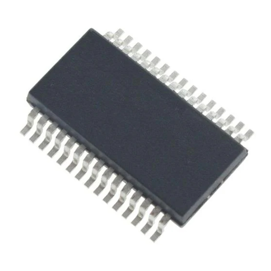
Page 18: Pin Configuration (Top View)
CHAPTER 1 GENERAL 1.4 Pin Configuration (Top View) 52-pin plastic LQFP (10 × 10) 52 51 50 49 48 47 46 45 44 43 42 41 40 RESET P81/S21 P60/TO40 P82/S20 P43/KR03 P83/S19 P42/KR02 P84/S18 P41/KR01 P85/S17 P40/KR00 INT/P61 14 15 16 17 18 19 20 21 22 23 24 25 26 Caution Connect the IC0 (Internally Connected) pin directly to V µ... - Page 19 CHAPTER 1 GENERAL COM0 to COM3: Common output S0 to S23: Segment output IC0: Internally connected SCK10: Serial clock input/output INT: Interrupt from peripherals SI10: Serial data input KR00 to KR03: Key return SO10: Serial data output P00 to P03: Port 0 TO40: Timer output...
-
Page 20: 0S Series Lineup
CHAPTER 1 GENERAL 1.5 78K/0S Series Lineup The products in the 78K/0S Series are listed below. The names enclosed in boxes are subseries names. Products in mass Products under production development Y subseries supports SMB. Small-scale package, general-purpose applications µ µ... - Page 21 CHAPTER 1 GENERAL The major differences between subseries are shown below. Series for General-Purpose and LCD Drive Function Timer 8-Bit 10-Bit Serial Interface Remarks Capacity Subseries 8-Bit 16-Bit Watch WDT MIN.Value (Bytes) µ − − − Small- PD789046 16 K 1 ch 1 ch 1 ch...
- Page 22 CHAPTER 1 GENERAL Series for ASSP Function Timer 8-Bit 10-Bit Serial Interface Remarks Capacity Subseries 8-Bit 16-Bit Watch WDT MIN.Value (Bytes) µ − − − − − PD789800 2 ch 1 ch 2 ch (USB: 1 ch) 4.0 V µ −...
-
Page 23: Block Diagram
CHAPTER 1 GENERAL 1.6 Block Diagram Port 0 P00 to P03 8-bit Cascaded timer 30 16-bit 8-bit timer TO40/P60 timer 40 P10, P11 Port 1 Port 2 P20 to P22 Watch timer 78K/0S (flash P40 to P43 CPU core Port 4 memory) Watchdog timer Port 6... -
Page 24: Overview Of Functions
CHAPTER 1 GENERAL 1.7 Overview of Functions µ µ µ µ µ PD789322 PD789324 PD789326 PD789327 PD78F9328 Part Number Item Internal memory Mask ROM Flash memory 4 KB 8 KB 16 KB 24 KB 32 KB High-speed RAM 256 bytes 512 bytes 24 ×... - Page 25 CHAPTER 1 GENERAL An outline of the timer is shown below. 8-Bit Timer 30 8-Bit Timer 40 Watch Timer Watchdog Timer Note 1 Note 2 Operation Interval timer 1 channel 1 channel 1 channel 1 channel mode External event counter –...
-
Page 26: Chapter 2 Pin Functions
CHAPTER 2 PIN FUNCTIONS 2.1 List of Pin Functions Port pins Pin Name Function After Reset Alternate Function − P00 to P03 Input/ Port 0. Input output This is a 4-bit I/O port. Input/output can be specified in 1-bit units. When used as an input port, on-chip pull-up resistors can be specified in port units using pull-up resistor option register 0 (PU0). - Page 27 CHAPTER 2 PIN FUNCTIONS Non-port pins Pin Name Function After Reset Alternate Function Input External interrupt input for which the valid edge (rising edge, Input falling edge, or both rising and falling edges) can be specified. KR00 to KR03 Input Key return signal detection Input P40 to P43...
-
Page 28: Description Of Pin Functions
CHAPTER 2 PIN FUNCTIONS 2.2 Description of Pin Functions 2.2.1 P00 to P03 (Port 0) These pins constitute a 4-bit I/O port and can be set in the input or output port mode in 1-bit units by port mode register 0 (PM0). When used as an input port, use of an on-chip pull-up resistor can be specified by pull-up resistor option register 0 (PU0) in port units. -
Page 29: P60, P61 (Port 6)
CHAPTER 2 PIN FUNCTIONS 2.2.5 P60, P61 (Port 6) These pins constitute a 2-bit I/O port. In addition, they also function as timer output and external interrupt input. Port 6 can be specified in the following operation mode in 1-bit units. Port mode In this mode, port 6 functions as a 2-bit I/O port. -
Page 30: X1, X2
CHAPTER 2 PIN FUNCTIONS 2.2.11 X1, X2 These pins are used to connect a crystal/ceramic resonator for main system clock oscillation. To supply an external clock, input the clock to X1 and input the inverted signal to X2. 2.2.12 XT1, XT2 These pins are used to connect a crystal resonator for subsystem clock oscillation. -
Page 31: Pin Input/Output Circuits And Recommended Connection Of Unused Pins
CHAPTER 2 PIN FUNCTIONS 2.3 Pin Input/Output Circuits and Recommended Connection of Unused Pins The input/output circuit type of each pin and recommended connection of unused pins are shown in Table 2-1. For the input/output circuit configuration of each type, see Figure 2-1. Table 2-1. - Page 32 CHAPTER 2 PIN FUNCTIONS Figure 2-1. I/O Circuit Type (2/2) Type 5-A Type 8 Pull-up P-ch enable Data P-ch IN/OUT Data P-ch Output N-ch IN/OUT disable Output N-ch disable Input enable Type 8-A Type 17-D P-ch Pull-up P-ch P-ch enable N-ch P-ch Data...
-
Page 33: Chapter 3 Cpu Architecture
CHAPTER 3 CPU ARCHITECTURE 3.1 Memory Space µ PD789327 Subseries can access 64 KB of memory space. Figures 3-1 through 3-5 show the memory maps. µ Figure 3-1. Memory Map ( PD789322) FFFFH Special function registers 256 × 8 bits FF00H FEFFH Internal high-speed RAM... - Page 34 CHAPTER 3 CPU ARCHITECTURE µ Figure 3-2. Memory Map ( PD789324) FFFFH Special function registers 256 × 8 bits FF00H FEFFH Internal high-speed RAM 256 × 8 bits FE00H FDFFH Reserved FA18H FA17H LCD display RAM 24 × 4 bits Data FA00H memory space...
- Page 35 CHAPTER 3 CPU ARCHITECTURE µ Figure 3-3. Memory Map ( PD789326) FFFFH Special function registers 256 × 8 bits FF00H FEFFH Internal high-speed RAM 512 × 8 bits FD00H FCFFH Reserved FA18H FA17H LCD display RAM 24 × 4 bits Data FA00H memory space...
- Page 36 CHAPTER 3 CPU ARCHITECTURE µ Figure 3-4. Memory Map ( PD789327) FFFFH Special function registers 256 × 8 bits FF00H FEFFH Internal high-speed RAM 512 × 8 bits FD00H FCFFH Reserved FA18H FA17H LCD display RAM 24 × 4 bits Data FA00H memory space...
- Page 37 CHAPTER 3 CPU ARCHITECTURE µ Figure 3-5. Memory Map ( PD78F9328) FFFFH Special function registers 256 × 8 bits FF00H FEFFH Internal high-speed RAM 512 × 8 bits FD00H FCFFH Reserved FA18H FA17H LCD display RAM 24 × 4 bits Data FA00H memory space...
-
Page 38: Internal Program Memory Space
CHAPTER 3 CPU ARCHITECTURE 3.1.1 Internal program memory space The internal program memory space stores programs and table data. This space is usually addressed by the program counter (PC). µ PD789327 Subseries provide internal ROM (or flash memory) with the following capacity for each product. Table 3-1. -
Page 39: Internal Data Memory (Internal High-Speed Ram) Space
CHAPTER 3 CPU ARCHITECTURE 3.1.2 Internal data memory (internal high-speed RAM) space µ PD789327 Subseries products incorporate the following RAM. Internal high-speed RAM µ Internal high-speed RAM is incorporated in the area between FE00H and FEFFH in the PD789322 and µ... -
Page 40: Data Memory Addressing
CHAPTER 3 CPU ARCHITECTURE 3.1.4 Data memory addressing µ PD789327 Subseries are provided with a variety of addressing modes to make memory manipulation as efficient as possible. At the addresses corresponding to data memory area especially, specific addressing modes that correspond to the particular function an area, such as the special function registers are available. - Page 41 CHAPTER 3 CPU ARCHITECTURE µ Figure 3-7. Data Memory Addressing ( PD789324) FFFFH Special function registers (SFRs) SFR addressing 256 × 8 bits FF20H FF1FH FF00H FEFFH Short direct Internal high-speed RAM addressing 256 × 8 bits FE20H FE1FH Direct addressing FE00H Register indirect FDFFH...
- Page 42 CHAPTER 3 CPU ARCHITECTURE µ Figure 3-8. Data Memory Addressing ( PD789326) FFFFH Special function registers (SFRs) SFR addressing 256 × 8 bits FF20H FF1FH FF00H FEFFH Short direct Internal high-speed RAM addressing 512 × 8 bits FE20H Direct addressing FE1FH FD00H Register indirect...
- Page 43 CHAPTER 3 CPU ARCHITECTURE µ Figure 3-9. Data Memory Addressing ( PD789327) FFFFH Special function registers (SFRs) SFR addressing 256 × 8 bits FF20H FF1FH FF00H FEFFH Short direct Internal high-speed RAM addressing 512 × 8 bits FE20H Direct addressing FE1FH FD00H Register indirect...
- Page 44 CHAPTER 3 CPU ARCHITECTURE µ Figure 3-10. Data Memory Addressing ( PD78F9328) FFFFH Special function registers (SFRs) SFR addressing 256 × 8 bits FF20H FF1FH FF00H FEFFH Short direct Internal high-speed RAM addressing 512 × 8 bits FE20H Direct addressing FE1FH FD00H Register indirect...
-
Page 45: Processor Registers
CHAPTER 3 CPU ARCHITECTURE 3.2 Processor Registers µ PD789327 Subseries provide the following on-chip processor registers. 3.2.1 Control registers The control registers contain special functions to control the program sequence statuses and stack memory. The program counter, program status word, and stack pointer are control registers. Program counter (PC) The program counter is a 16-bit register that holds the address information of the next program to be executed. - Page 46 CHAPTER 3 CPU ARCHITECTURE Interrupt enable flag (IE) This flag controls interrupt request acknowledgement operations of the CPU. When 0, IE is set to the interrupt disable status (DI), and interrupt requests other than non-maskable interrupt are all disabled. When 1, IE is set to the interrupt enable status (EI). Interrupt request acknowledgement enable is controlled with an interrupt mask flag for various interrupt sources.
- Page 47 CHAPTER 3 CPU ARCHITECTURE Stack pointer (SP) This is a 16-bit register to hold the start address of the memory stack area. Only the internal high-speed RAM area can be set as the stack area. Figure 3-13. Stack Pointer Configuration SP15 SP14 SP13 SP12 SP11 SP10...
-
Page 48: General-Purpose Registers
CHAPTER 3 CPU ARCHITECTURE 3.2.2 General-purpose registers The general-purpose registers consist of eight 8-bit registers (X, A, C, B, E, D, L, and H). Each register can be used as an 8-bit register, or two 8-bit registers in pairs can be used as a 16-bit register (AX, BC, DE, and HL). -
Page 49: Special Function Registers (Sfrs)
CHAPTER 3 CPU ARCHITECTURE 3.2.3 Special function registers (SFRs) Unlike a general-purpose register, each special function register has a special function. The special function registers are allocated in the 256-byte area of FF00H to FFFFH. Special function registers can be manipulated, like general-purpose registers, by operation, transfer, and bit manipulation instructions. - Page 50 CHAPTER 3 CPU ARCHITECTURE Table 3-3. Special Function Registers (1/2) Address Special Function Register (SFR) Name Symbol Bit Unit for Manipulation After Reset 1 Bit 8 Bits 16 Bits √ √ − FF00H Port 0 √ √ − FF01H Port 1 √...
- Page 51 CHAPTER 3 CPU ARCHITECTURE Table 3-3. Special Function Registers (2/2) Address Special Function Register (SFR) Name Symbol Bit Unit for Manipulation After Reset 1 Bit 8 Bits 16 Bits √ √ − FFE0H Interrupt request flag register 0 √ √ −...
-
Page 52: Instruction Address Addressing
CHAPTER 3 CPU ARCHITECTURE 3.3 Instruction Address Addressing An instruction address is determined by the program counter (PC) contents. The PC contents are normally incremented (+1 for each byte) automatically according to the number of bytes of an instruction to be fetched each time another instruction is executed. -
Page 53: Immediate Addressing
CHAPTER 3 CPU ARCHITECTURE 3.3.2 Immediate addressing [Function] Immediate data in the instruction word is transferred to the program counter (PC) and branched. This function is carried out when the CALL !addr16 or BR !addr16 instruction is executed. CALL !addr16 and BR !addr16 instructions can be branched to any location in the memory space. [Illustration] In case of CALL !addr16 and BR !addr16 instructions CALL or BR... -
Page 54: Register Addressing
CHAPTER 3 CPU ARCHITECTURE 3.3.3 Table indirect addressing [Function] Table contents (branch destination address) of the particular location to be addressed by the lower 5-bit immediate data of an instruction code from bit 1 to bit 5 are transferred to the program counter (PC) and branched. -
Page 55: Operand Address Addressing
CHAPTER 3 CPU ARCHITECTURE 3.4 Operand Address Addressing The following various methods are available to specify the register and memory (addressing) which undergo manipulation during instruction execution. 3.4.1 Direct addressing [Function] The memory indicated with immediate data in an instruction word is directly addressed. [Operand format] Identifier Description... -
Page 56: Short Direct Addressing
CHAPTER 3 CPU ARCHITECTURE 3.4.2 Short direct addressing [Function] The memory to be manipulated in the fixed space is directly addressed with 8-bit data in an instruction word. The fixed space is the 256-byte space FE20H to FF1FH where the addressing is applied. Internal high-speed RAM and special function registers (SFRs) are mapped at FE20H to FEFFH and FF00H to FF1FH, respectively. -
Page 57: Special Function Register (Sfr) Addressing
CHAPTER 3 CPU ARCHITECTURE 3.4.3 Special function register (SFR) addressing [Function] The memory-mapped special function registers (SFRs) are addressed with 8-bit immediate data in an instruction word. This addressing is applied to the 256-byte space FF00H to FFFFH. However, the SFRs mapped at FF00H to FF1FH can also be accessed with short direct addressing. -
Page 58: Register Addressing
CHAPTER 3 CPU ARCHITECTURE 3.4.4 Register addressing [Function] In the register addressing mode, general-purpose registers are accessed as operands. The general-purpose register to be accessed is specified by a register specification code or functional name in the instruction code. Register addressing is carried out when an instruction with the following operand format is executed. When an 8-bit register is specified, one of the eight registers is specified with 3 bits in the instruction code. -
Page 59: Register Indirect Addressing
CHAPTER 3 CPU ARCHITECTURE 3.4.5 Register indirect addressing [Function] In the register indirect addressing mode, memory is manipulated according to the contents of a register pair specified as an operand. The register pair to be accessed is specified by the register pair specification code in an instruction code. -
Page 60: Based Addressing
CHAPTER 3 CPU ARCHITECTURE 3.4.6 Based addressing [Function] 8-bit immediate data is added to the contents of the base register, that is, the HL register pair, and the sum is used to address the memory. Addition is performed by expanding the offset data as a positive number to 16 bits. -
Page 61: Chapter 4 Port Functions
CHAPTER 4 PORT FUNCTIONS 4.1 Port Functions µ PD789327 Subseries provide the ports shown in Figure 4-1, enabling various methods of control. Numerous other functions are provided that can be used in addition to the digital I/O port functions. For more information on these additional functions, see CHAPTER 2 PIN FUNCTIONS. -
Page 62: Port Configuration
CHAPTER 4 PORT FUNCTIONS Table 4-1. Port Functions Port Name Pin Name Function Port 0 P00 to P03 This is an I/O port for which input and output can be specified in 1-bit units. When used as an input port, on-chip pull-up resistors can be specified using pull-up resistor option register 0 (PU0). -
Page 63: Port 0
CHAPTER 4 PORT FUNCTIONS 4.2.1 Port 0 Port 0 is a 4-bit I/O port with an output latch. It can be specified in the input or output mode in 1-bit units by using the port mode register 0 (PM0). When the P00 to P03 pins are used as input port pins, on-chip pull-up resistors can be connected in 4-bit units by using pull-up resistor option register 0 (PU0). -
Page 64: Port 1
CHAPTER 4 PORT FUNCTIONS 4.2.2 Port 1 Port 1 is a 2-bit I/O port with an output latch. It can be specified in the input or output mode in 1-bit units by using port mode register 1 (PM1). When using the P10 and P11 pins as input port pins, on-chip pull-up resistors can be connected in 2-bit units by using pull-up resistor option register 0 (PU0). -
Page 65: Port 2
CHAPTER 4 PORT FUNCTIONS 4.2.3 Port 2 Port 2 is a 3-bit I/O port with an output latch. It can be specified in the input or output mode in 1-bit units by using port mode register 2 (PM2). On-chip pull-up resistors can be connected in 1-bit units by using pull-up resistor option register B2 (PUB2) regardless of whether the port is in the input or output mode. - Page 66 CHAPTER 4 PORT FUNCTIONS Figure 4-5. Block Diagram of P21 PUB2 PUB21 P-ch PORT Output latch P21/SO10 (P21) PM21 Alternate function PUB2: Pull-up resistor option register B2 Port mode register Port 2 read signal Port 2 write signal User’s Manual U15043EJ3V1UD...
- Page 67 CHAPTER 4 PORT FUNCTIONS Figure 4-6. Block Diagram of P22 PUB2 PUB22 P-ch Alternate function PORT Output latch P22/SI10 (P22) PM22 PUB2: Pull-up resistor option register B2 Port mode register Port 2 read signal Port 2 write signal User’s Manual U15043EJ3V1UD...
-
Page 68: Port 4
CHAPTER 4 PORT FUNCTIONS 4.2.4 Port 4 Port 4 is a 4-bit I/O port with an output latch. It can be specified in the input or output mode in 1-bit units by using port mode register 4 (PM4). When using the P40 to P43 pins as input port pins, on-chip pull-up resistors can be connected in 4-bit units by using pull-up resistor option register 0 (PU0). -
Page 69: Port 6
CHAPTER 4 PORT FUNCTIONS 4.2.5 Port 6 Port 6 is a 2-bit I/O port with an output latch. It can be specified in the input or output mode in 1-bit units by using port mode register 6 (PM6). This port is also used as a timer output and external interrupt input. RESET input sets port 6 in the input mode. - Page 70 CHAPTER 4 PORT FUNCTIONS Figure 4-9. Block Diagram of P61 Alternate function PORT Output latch P61/INT (P61) PM61 Port mode register Port 6 read signal Port 6 write signal User’s Manual U15043EJ3V1UD...
-
Page 71: Port 8
CHAPTER 4 PORT FUNCTIONS 4.2.6 Port 8 Port 8 is a 6-bit I/O port with an output latch. It can be specified in the input or output mode in 1-bit units by using port mode register 8 (PM8). This port is also used as a segment output, and can be switched to the port function or segment output function in 1-bit units by port function register 8 (PF8). -
Page 72: Registers Controlling Port Function
CHAPTER 4 PORT FUNCTIONS 4.3 Registers Controlling Port Function The ports are controlled by the following three types of registers. • Port mode registers (PM0 to PM2, PM4, PM6, PM8) • Pull-up resistor option registers (PU0, PUB2) • Port function register 8 (PF8) Port mode registers (PM0 to PM2, PM4, PM6, PM8) PM0 to PM2, PM4, PM6 and PM8 are used to set port input/output in 1-bit units. - Page 73 CHAPTER 4 PORT FUNCTIONS Table 4-3. Port Mode Registers and Output Latch Settings When Using Alternate Functions PM×× P×× Pin Name Alternate Function Name × SCK10 Input Output SO10 Output × SI10 Input × P40 to P43 KR00 to KR03 Input TO40 Output...
- Page 74 CHAPTER 4 PORT FUNCTIONS Pull-up resistor option register B2 (PUB2) PUB2 sets whether on-chip pull-up resistors on P20 to P22 are used or not in bit units. A pin for which use of an on-chip pull-up resistor is specified by PUB2 can be connected to the pull-up resistor regardless of whether the pin is in the input or output mode.
- Page 75 CHAPTER 4 PORT FUNCTIONS Figure 4-14. Format of Port Function Register 8 Symbol Address After reset PF85 PF84 PF83 PF82 PF81 PF80 FF58H PF8n P8n port function (n = 0 to 5) Operates as a general-purpose port Operates as an LCD segment signal output Cautions 1.
-
Page 76: Port Function Operation
CHAPTER 4 PORT FUNCTIONS 4.4 Port Function Operation The operation of a port differs depending on whether the port is set in the input or output mode, as described below. 4.4.1 Writing to I/O port In output mode A value can be written to the output latch of a port by using a transfer instruction. The contents of the output latch can be output from the pins of the port. -
Page 77: Chapter 5 Clock Generator
CHAPTER 5 CLOCK GENERATOR 5.1 Clock Generator Functions The clock generator generates the clock to be supplied to the CPU and peripheral hardware. The following two types of system clock oscillators are used. • Main system clock (ceramic/crystal) oscillator This circuit oscillates at 1.0 to 5.0 MHz. Oscillation can be stopped by executing the STOP instruction or setting the processor clock control register (PCC). - Page 78 CHAPTER 5 CLOCK GENERATOR Figure 5-1. Block Diagram of Clock Generator Internal bus Suboscillation mode register FRC SCC (SCKM) Subsystem clock Watch timer oscillator LCD controller/driver Main system Clock to peripheral clock Prescaler hardware oscillator CPU clock Standby Wait controller controller STOP MCC PCC1...
-
Page 79: Registers Controlling Clock Generator
CHAPTER 5 CLOCK GENERATOR 5.3 Registers Controlling Clock Generator The clock generator is controlled by the following three registers. • Processor clock control register (PCC) • Suboscillation mode register (SCKM) • Subclock control register (CSS) Processor clock control register (PCC) PCC sets CPU clock selection and the division ratio. - Page 80 CHAPTER 5 CLOCK GENERATOR Suboscillation mode register (SCKM) SCKM selects a feedback resistor for the subsystem clock, and controls the oscillation of the clock. SCKM is set with a 1-bit or 8-bit memory manipulation instruction. RESET input clears SCKM to 00H. Figure 5-3.
-
Page 81: System Clock Oscillators
CHAPTER 5 CLOCK GENERATOR 5.4 System Clock Oscillators 5.4.1 Main system clock oscillator The main system clock oscillator is oscillated by the crystal or ceramic resonator (5.0 MHz TYP.) connected across the X1 and X2 pins. An external clock can also be input to the circuit. In this case, input the clock signal to the X1 pin, and input the inverted signal to the X2 pin. -
Page 82: Subsystem Clock Oscillator
CHAPTER 5 CLOCK GENERATOR 5.4.2 Subsystem clock oscillator The subsystem clock oscillator is oscillated by the crystal resonator (32.768 kHz TYP.) connected across the XT1 and XT2 pins. An external clock can also be input to the circuit. In this case, input the clock signal to the XT1 pin, and input the inverted signal to the XT2 pin. -
Page 83: Example Of Incorrect Resonator Connection
CHAPTER 5 CLOCK GENERATOR 5.4.3 Example of incorrect resonator connection Figure 5-7 shows examples of incorrect resonator connection. Figure 5-7. Examples of Incorrect Resonator Connection (1/2) (a) Too long wiring (b) Crossed signal line PORTn (n = 0 to 2, 4, 6, 8) (c) Wiring near high fluctuating current (d) Current flowing through ground line of oscillator (potential at points A, B, and C fluctuates) -
Page 84: Divider Circuit
CHAPTER 5 CLOCK GENERATOR Figure 5-7. Examples of Incorrect Resonator Connection (2/2) (e) Signal is fetched (f) Parallel and near signal lines of main system clock and subsystem clock XT2 is wired parallel to X1. Remark When using the subsystem clock, read X1 and X2 as XT1 and XT2, respectively, and connect a resistor to the XT2 in series. -
Page 85: Clock Generator Operation
CHAPTER 5 CLOCK GENERATOR 5.5 Clock Generator Operation The clock generator generates the following clocks and controls the operation modes of the CPU, such as the standby mode. • Main system clock • Subsystem clock • CPU clock • Clock to peripheral hardware The operation and function of the clock generator is determined by the processor clock control register (PCC), suboscillation mode register (SCKM), and subclock control register (CSS), as follows. -
Page 86: Changing Setting Of System Clock And Cpu Clock
CHAPTER 5 CLOCK GENERATOR 5.6 Changing Setting of System Clock and CPU Clock 5.6.1 Time required for switching between system clock and CPU clock The CPU clock can be selected by using bit 1 (PCC1) of the processor clock control register (PCC) and bit 4 (CSS0) of the subclock control register (CSS). -
Page 87: Switching Between System Clock And Cpu Clock
CHAPTER 5 CLOCK GENERATOR 5.6.2 Switching between system clock and CPU clock The following figure illustrates how the CPU clock and system clock switch. Figure 5-8. Example of Switching Between System Clock and CPU Clock RESET Input request signal rewrite rewrite rewrite System clock... -
Page 88: Chapter 6 8-Bit Timers 30 And 40
CHAPTER 6 8-BIT TIMERS 30 AND 40 6.1 8-Bit Timers 30 and 40 Functions µ The 8-bit timer in the PD789327 Subseries has 2 channels (timer 30 and timer 40). The operation modes listed in the following table can be set via mode register settings. Table 6-1. -
Page 89: 8-Bit Timers 30 And 40 Configuration
CHAPTER 6 8-BIT TIMERS 30 AND 40 6.2 8-Bit Timers 30 and 40 Configuration The 8-bit timers 30 and 40 include the following hardware. Table 6-2. Configuration of 8-Bit Timers 30 and 40 Item Configuration 8 bits × 2 (TM30, TM40) Timer counters Compare registers: 8 bits ×... - Page 90 Figure 6-1. Block Diagram of Timer 30 Internal bus 8-bit timer mode control register 30 (TMC30) TCE30 TCL301 TCL300 TMD300 8-bit compare register 30 Decoder (CR30) Selector To Figure 6-2 (G) Match Timer 30 match signal Bit 7 of TM40 (in carrier generator mode) (from Figure 6-2 (A)) 8-bit timer counter 30...
- Page 91 Figure 6-2. Block Diagram of Timer 40 Internal bus Carrier generator output 8-bit timer mode control control register 40 (TCA40) register 40 (TMC40) 8-bit compare 8-bit H width compare RMC40 NRZB40 NRZ40 TCE40 TCL402 TCL401 TCL400 TMD401 TMD400 TOE40 register 40 (CR40) register 40 (CRH40) Decoder From Figure 6-1 (G)
- Page 92 CHAPTER 6 8-BIT TIMERS 30 AND 40 Figure 6-3. Block Diagram of Output Controller (Timer 40) TOE40 RMC40 NRZ40 output latch PM60 TO40/P60 Carrier clock Carrier generator mode (1) 8-bit compare register 30 (CR30) This 8-bit register is used to continually compare the value set to CR30 with the count value in 8-bit timer counter 30 (TM30) and to generate an interrupt request (INTTM30) when a match occurs.
- Page 93 CHAPTER 6 8-BIT TIMERS 30 AND 40 (4) 8-bit timer counters 30 and 40 (TM30 and TM40) These are 8-bit registers that are used to count the count pulse. TM30 and TM40 are read with an 8-bit memory manipulation instruction. RESET input sets TM30 and TM40 to 00H.
-
Page 94: Registers Controlling 8-Bit Timers 30 And 40
CHAPTER 6 8-BIT TIMERS 30 AND 40 6.3 Registers Controlling 8-Bit Timers 30 and 40 8-bit timer 30 and 40 are controlled by the following five registers. • 8-bit timer mode control register 30 (TMC30) • 8-bit timer mode control register 40 (TMC40) •... - Page 95 CHAPTER 6 8-BIT TIMERS 30 AND 40 (1) 8-bit timer mode control register 30 (TMC30) 8-bit timer mode control register 30 (TMC30) is used to control the timer 30 count clock setting and the operation mode setting. TMC30 is set with a 1-bit or 8-bit memory manipulation instruction. RESET input sets TMC30 to 00H.
- Page 96 CHAPTER 6 8-BIT TIMERS 30 AND 40 (2) 8-bit timer mode control register 40 (TMC40) 8-bit timer mode control register 40 (TMC40) is used to control the timer 40 count clock setting and the operation mode setting. TMC40 is set with a 1-bit or 8-bit memory manipulation instruction. RESET input sets TMC40 to 00H.
- Page 97 CHAPTER 6 8-BIT TIMERS 30 AND 40 (3) Carrier generator output control register 40 (TCA40) This register is used to set the timer output data in carrier generator mode. TCA40 is set with an 8-bit memory manipulation instruction. RESET input sets TCA40 to 00H. Figure 6-6.
- Page 98 CHAPTER 6 8-BIT TIMERS 30 AND 40 (4) Port mode register 6 (PM6) This register is used to set the I/O mode of port 6 in 1-bit units. When using the P60/TO40 pin as a timer output, set the PM60 and P60 output latch to 0. PM6 is set with a 1-bit or 8-bit memory manipulation instruction.
-
Page 99: 8-Bit Timers 30 And 40 Operation
CHAPTER 6 8-BIT TIMERS 30 AND 40 6.4 8-Bit Timers 30 and 40 Operation 6.4.1 Operation as 8-bit timer counter Timers 30 and 40 can be independently used as 8-bit timer counters. The following modes can be used for the 8-bit timer counters. •... - Page 100 CHAPTER 6 8-BIT TIMERS 30 AND 40 Table 6-3. Interval Time of Timer 30 (at f = 5.0 MHz Operation) TCL301 TCL300 Minimum Interval Time Maximum Interval Time Resolution µ µ (12.8 (12.8 (3.28 ms) µ µ (51.2 (13.1 ms) (51.2 Input cycle of timer 40 match Input cycle of timer 40 match...
- Page 101 CHAPTER 6 8-BIT TIMERS 30 AND 40 Figure 6-9. Timing of Interval Timer Operation with 8-Bit Resolution (When CRn0 Is Set to 00H) Count clock TMn0 CRn0 TCEn0 Count start INTTMn0 TOn0 Remark n = 3, 4 Figure 6-10. Timing of Interval Timer Operation with 8-Bit Resolution (When CRn0 Is Set to FFH) Count clock TMn0 Clear...
- Page 102 CHAPTER 6 8-BIT TIMERS 30 AND 40 Figure 6-11. Timing of Interval Timer Operation with 8-Bit Resolution (When CRn0 Changes from N to M (N < M)) Count clock TMn0 Clear Clear Clear CRn0 TCEn0 Count start INTTMn0 Interrupt acknowledgment Interrupt acknowledgment TOn0 CRn0 overwritten...
- Page 103 CHAPTER 6 8-BIT TIMERS 30 AND 40 Figure 6-13. Timing of Interval Timer Operation with 8-Bit Resolution (When Timer 40 Match Signal Is Selected for Timer 30 Count Clock) Timer 40 count clock TM40 Clear Clear Clear Clear CR40 TCE40 Count start INTTM40 Input clock to timer 30...
- Page 104 CHAPTER 6 8-BIT TIMERS 30 AND 40 Operation as square-wave output with 8-bit resolution (timer 40 only) Square waves of any frequency can be output at an interval specified by the value preset in 8-bit compare register 40 (CR40). To operate timer 40 for square-wave output, settings must be made in the following sequence. <1>...
- Page 105 CHAPTER 6 8-BIT TIMERS 30 AND 40 Figure 6-14. Timing of Square-Wave Output with 8-Bit Resolution Count clock TM40 Clear Clear Clear CR40 TCE40 Count start INTTM40 Interrupt acknowledgment Interrupt acknowledgment Interrupt acknowldgement Note TO40 Square-wave output cycle Note The initial value of TO40 is low level when output is enabled (TOE40 = 1). Square-wave output cycle = 2 (N + 1) ×...
-
Page 106: Operation As 16-Bit Timer Counter
CHAPTER 6 8-BIT TIMERS 30 AND 40 6.4.2 Operation as 16-bit timer counter Timers 30 and 40 can be used as 16-bit timer counters via a cascade connection. In this case, 8-bit timer counter 30 (TM30) is the higher 8 bits and 8-bit timer counter 40 (TM40) is the lower 8 bits. 8-bit timer 40 controls reset and clear. - Page 107 Figure 6-15. Timing of Interval Timer Operation with 16-Bit Resolution TM40 count clock TM40 count value FFH 00H 7FH 80H FFH 00H 7FH 80H FFH 00H Not cleared because TM30 does not match Cleared because TM30 and TM40 match simultaneously CR40 TCE40 Count start...
- Page 108 CHAPTER 6 8-BIT TIMERS 30 AND 40 Operation as square-wave output with 16-bit resolution Square waves of any frequency can be output at an interval specified by the count value preset in CR30 and CR40. To operate as a square-wave output with 16-bit resolution, settings must be made in the following sequence. <1>...
- Page 109 Figure 6-16. Timing of Square-Wave Output with 16-Bit Resolution TM40 count clock TM40 count clock FFH 00H 7FH 80H FFH 00H 7FH 80H FFH 00H Not cleared because TM30 does not match Cleared because TM30 and TM40 match simultaneously CR40 TCE40 Count start TM30 count clock...
-
Page 110: Operation As Carrier Generator
CHAPTER 6 8-BIT TIMERS 30 AND 40 6.4.3 Operation as carrier generator An arbitrary carrier clock generated by TM40 can be output in the cycle set in TM30. To operate timers 30 and 40 as carrier generators, settings must be made in the following sequence. <1>... - Page 111 CHAPTER 6 8-BIT TIMERS 30 AND 40 Figures 6-17 to 6-19 show the operation timing of the carrier generator. Figure 6-17. Timing of Carrier Generator Operation (When CR40 = N, CRH40 = M (M > N)) TM40 count clock TM40 count value Clear Clear...
- Page 112 CHAPTER 6 8-BIT TIMERS 30 AND 40 Figure 6-18. Timing of Carrier Generator Operation (When CR40 = N, CRH40 = M (M < N)) TM40 count clock TM40 count value Clear Clear Clear Clear CR40 CRH40 TCE40 Count start INTTM40 Carrier clock TM30 count clock TM30...
- Page 113 CHAPTER 6 8-BIT TIMERS 30 AND 40 Figure 6-19. Timing of Carrier Generator Operation (When CR40 = CRH40 = N) TM40 count clock TM40 count value Clear Clear Clear Clear Clear CR40 CRH40 TCE40 Count start INTTM40 Carrier clock TM30 count clock TM30 CR30 TCE30...
-
Page 114: Operation As Pwm Output (Timer 40 Only)
CHAPTER 6 8-BIT TIMERS 30 AND 40 6.4.4 Operation as PWM output (timer 40 only) In the PWM output mode, a pulse of any duty ratio can be output by setting a low-level width using CR40 and a high-level width using CRH40. To operate timer 40 in PWM output mode, settings must be made in the following sequence. - Page 115 CHAPTER 6 8-BIT TIMERS 30 AND 40 Figure 6-20. PWM Output Mode Timing (Basic Operation) TM40 count clock TM40 count value Clear Clear Clear Clear CR40 CRH40 TCE40 Count start INTTM40 Note TO40 Note The initial value of TO40 is low level when output is enabled (TOE40 = 1). Figure 6-21.
-
Page 116: Notes On Using 8-Bit Timers 30 And 40
CHAPTER 6 8-BIT TIMERS 30 AND 40 6.5 Notes on Using 8-Bit Timers 30 and 40 Error on starting timer An error of up to 1.5 clocks is included in the time between when the timer is started and a match signal is generated. -
Page 117: Chapter 7 Watch Timer
CHAPTER 7 WATCH TIMER 7.1 Watch Timer Functions The watch timer has the following functions. • Watch timer • Interval timer The watch and interval timers can be used at the same time. Figure 7-1 shows a block diagram of the watch timer. Figure 7-1. -
Page 118: Watch Timer Configuration
CHAPTER 7 WATCH TIMER Watch timer The 4.19 MHz main system clock or 32.768 kHz subsystem clock is used to generate an interrupt request (INTWT) at 0.5-second intervals. Caution When the main system clock is operating at 5.0 MHz, it cannot be used to generate a 0.5- second interval. -
Page 119: Register Controlling Watch Timer
CHAPTER 7 WATCH TIMER 7.3 Register Controlling Watch Timer The watch timer mode control register (WTM) is used to control the watch timer. • Watch timer mode control register (WTM) WTM selects a count clock for the watch timer and specifies whether to enable clocking of the timer. It also specifies the prescaler interval and how the 5-bit counter is controlled. -
Page 120: Watch Timer Operation
CHAPTER 7 WATCH TIMER 7.4 Watch Timer Operation 7.4.1 Operation as watch timer The main system clock (4.19 MHz) or subsystem clock (32.768 kHz) is used as a watch timer which generates 0.5-second intervals. The watch timer is used to generate an interrupt request at specified intervals. By setting bits 0 and 1 (WTM0 and WTM1) of the watch timer mode control register (WTM) to 1, the watch timer starts counting. - Page 121 CHAPTER 7 WATCH TIMER Figure 7-3. Watch Timer/Interval Timer Operation Timing 5-bit counter Overflow Overflow Start Count clock Watch timer interrupt INTWT Watch timer interrupt time (0.5 s) Watch timer interrupt time (0.5 s) Interval timer interrupt INTWTI Interval timer (T) Caution When operation of the watch timer and 5-bit counter has been enabled by setting the watch timer mode control register (WTM) (setting WTM0 (bit 0 of WTM) to 1), the time until the first interrupt request after this setting will not be exactly the same as the watch timer interrupt time...
-
Page 122: Chapter 8 Watchdog Timer
CHAPTER 8 WATCHDOG TIMER 8.1 Watchdog Timer Functions The watchdog timer has the following functions. • Watchdog timer • Interval timer Caution Select the watchdog timer mode or interval timer mode by using the watchdog timer mode register (WDTM). Watchdog timer The watchdog timer is used to detect inadvertent program loop. -
Page 123: Watchdog Timer Configuration
CHAPTER 8 WATCHDOG TIMER 8.2 Watchdog Timer Configuration The watchdog timer includes the following hardware. Table 8-3. Configuration of Watchdog Timer Item Configuration Control registers Watchdog timer clock selection register (TCL2) Watchdog timer mode register (WDTM) Figure 8-1. Block Diagram of Watchdog Timer Internal bus WDTMK Prescaler... -
Page 124: Registers Controlling Watchdog Timer
CHAPTER 8 WATCHDOG TIMER 8.3 Registers Controlling Watchdog Timer The watchdog timer is controlled by the following two registers. • Watchdog timer clock selection register (TCL2) • Watchdog timer mode register (WDTM) Watchdog timer clock selection register (TCL2) TCL2 sets the watchdog timer count clock. This register is set with an 8-bit memory manipulation instruction. - Page 125 CHAPTER 8 WATCHDOG TIMER Watchdog timer mode register (WDTM) WDTM sets an operation mode of the watchdog timer, and enables/disables counting of the watchdog timer. This register is set with a 1-bit or 8-bit memory manipulation instruction. RESET input clears WDTM to 00H. Figure 8-3.
-
Page 126: Watchdog Timer Operation
CHAPTER 8 WATCHDOG TIMER 8.4 Watchdog Timer Operation 8.4.1 Operation as watchdog timer The watchdog timer detects an inadvertent program loop when bit 4 (WDTM4) of the watchdog timer mode register (WDTM) is set to 1. The count clock (inadvertent program loop detection time interval) of the watchdog timer can be selected by bits 1 and 2 (TCL21 and TCL22) of the watchdog timer clock selection register (TCL2). -
Page 127: Operation As Interval Timer
CHAPTER 8 WATCHDOG TIMER 8.4.2 Operation as interval timer When bit 4 (WDTM4) and bit 3 (WDTM3) of the watchdog timer mode register (WDTM) are set to 0 and 1, respectively, the watchdog timer also operates as an interval timer that repeatedly generates an interrupt at time intervals specified by a preset count value. -
Page 128: Chapter 9 Serial Interface 10
CHAPTER 9 SERIAL INTERFACE 10 9.1 Serial Interface 10 Functions Serial interface 10 has the following two modes. • Operation stop mode • 3-wire serial I/O mode Operation stop mode This mode is used when serial transfer is not carried out. It enables a reduction in power consumption. 3-wire serial I/O mode (MSB/LSB-first switchable) In this mode, 8-bit data transfer is carried out-first with three lines, one for the serial clock (SCK10) and two for serial data (SI10 and SO10). -
Page 129: Serial Interface 10 Configuration
CHAPTER 9 SERIAL INTERFACE 10 9.2 Serial Interface 10 Configuration Serial interface 10 includes the following hardware. Table 9-1. Configuration of Serial Interface 10 Item Configuration Register Transmit/receive shift register 10 (SIO10) Control register Serial operation mode register 10 (CSIM10) Port mode register 2 (PM2) Port 2 (P2) Transmit/receive shift register 10 (SIO10) - Page 130 Figure 9-1. Block Diagram of Serial Interface 10 Internal bus Serial operation mode register 10 (CSIM10) CSIE10 TPS101 TPS100 DIR10 CSCK10 Transmit/receive shift register 10 (SIO10) SI10/P22 SO10/P21 PM21 output latch (P21) Interrupt request Serial clock counter INTCSI10 generator output latch (P20) PM20 Clock controller...
-
Page 131: Registers Controlling Serial Interface 10
CHAPTER 9 SERIAL INTERFACE 10 9.3 Registers Controlling Serial Interface 10 Serial interface 10 is controlled by the following three registers. • Serial operation mode register 10 (CSIM10) • Port mode register 2 (PM2) • Port 2 (P2) Serial operation mode register 10 (CSIM10) CSIM10 is used to control serial interface 10 and set the serial clock and start bit. - Page 132 CHAPTER 9 SERIAL INTERFACE 10 (2) Port mode register 2 (PM2) This register is used to set the I/O mode of port 2 in 1-bit units. PM2 is set with a 1-bit or 8-bit memory manipulation instruction. RESET input sets PM2 to FFH. Figure 9-3.
-
Page 133: Serial Interface 10 Operation
CHAPTER 9 SERIAL INTERFACE 10 9.4 Serial Interface 10 Operation Serial interface 10 provides the following two types of modes. • Operation stop mode • 3-wire serial I/O mode 9.4.1 Operation stop mode In the operation stop mode, serial transfer is not executed, therefore enabling a reduction in the power consumption. -
Page 134: 3-Wire Serial I/O Mode
CHAPTER 9 SERIAL INTERFACE 10 9.4.2 3-wire serial I/O mode The 3-wire serial I/O mode is useful for connection of peripheral I/O and display controllers, etc., which incorporate a conventional clocked serial interface, such as the 75XL Series, 78K Series, 17K Series. Communication is performed using three lines: a serial clock line (SCK10), serial output line (SO10), and serial input line (SI10). - Page 135 CHAPTER 9 SERIAL INTERFACE 10 Communication operation In the 3-wire serial I/O mode, data transmission/reception is performed in 8-bit units. Data is transmitted/received bit by bit in synchronization with the serial clock. Transmit shift register 10 (SIO10) shift operations are performed in synchronization with the fall of the serial clock (SCK10).
-
Page 136: Chapter 10 Lcd Controller/Driver
CHAPTER 10 LCD CONTROLLER/DRIVER 10.1 LCD Controller/Driver Functions µ The functions of the LCD controller/driver of the PD789327 Subseries are as follows. Automatic output of segment and common signals based on automatic display data memory read Two different display modes: •... - Page 137 Figure 10-1. Block Diagram of LCD Controller/Driver Internal bus LCD clock control LCD display mode Display data memory register 0 (LCDC0) register 0 (LCDM0) FA00H FA11H FA16H FA17H LCDC03 LCDC02 LCDC01 LCDC00 LCDON0 VAON0 LCDM02 3 2 1 0 3 2 1 0 3 2 1 0 6 5 4 3 2 1 0...
-
Page 138: Registers Controlling Lcd Controller/Driver
CHAPTER 10 LCD CONTROLLER/DRIVER 10.3 Registers Controlling LCD Controller/Driver • LCD display mode register 0 (LCDM0) • LCD clock control register 0 (LCDC0) • Port function register 8 (PF8) LCD display mode register 0 (LCDM0) LCDM0 specifies whether to enable display operation. It also specifies the operation mode and display mode. This register is set with a 1-bit or 8-bit memory manipulation instruction. - Page 139 CHAPTER 10 LCD CONTROLLER/DRIVER Figure 10-2. Format of LCD Display Mode Register 0 Symbol <7> <6> Address After reset LCDM0 LCDON0 VAON0 LCDM02 FFB0H LCDON0 LCD display enable/disable Display off (all segment outputs are unselected for signal output) Display on Note 1 VAON0 LCD controller/driver operation mode...
- Page 140 CHAPTER 10 LCD CONTROLLER/DRIVER LCD clock control register 0 (LCDC0) LCDC0 specifies the LCD source clock and LCD clock. The frame frequency is determined by the LCD clock and the number of time divisions. This register is set with a 1-bit or 8-bit memory manipulation instruction. RESET input clears LCDC0 to 00H.
- Page 141 CHAPTER 10 LCD CONTROLLER/DRIVER Port function register 8 (PF8) PF8 specifies whether S17/P85 to S22/P80 are used as LCD segment signal outputs or general-purpose ports in 1-bit units. This register is set with a 1-bit or 8-bit memory manipulation instruction. RESET input clears PF8 to 00H.
-
Page 142: Setting Lcd Controller/Driver
CHAPTER 10 LCD CONTROLLER/DRIVER Remark Sm: LCD segment output (m = 22 to 17) P8n: Bit n of Port 8 (n = 0 to 5) PF8n: Bit n of Port function register 8 (n = 0 to 5) Port 8 read signal 10.4 Setting LCD Controller/Driver Set the LCD controller/driver using the following procedure. -
Page 143: Lcd Display Data Memory
CHAPTER 10 LCD CONTROLLER/DRIVER 10.5 LCD Display Data Memory The LCD display data memory is mapped at addresses FA00H to FA17H. Data in the LCD display data memory can be displayed on the LCD panel using the LCD controller/driver. Figure 10-5 shows the relationship between the contents of the LCD display data memory and the segment/common outputs. -
Page 144: Common And Segment Signals
CHAPTER 10 LCD CONTROLLER/DRIVER 10.6 Common and Segment Signals Each pixel of the LCD panel turns on when the potential difference between the corresponding common and segment signals becomes higher than a specific voltage (LCD drive voltage, V ). It turns off when the potential difference becomes lower than V Applying DC voltage to the common and segment signals for an LCD panel would deteriorate it. - Page 145 CHAPTER 10 LCD CONTROLLER/DRIVER Table 10-5. LCD Drive Voltage (a) Static display mode Segment Signal Select Signal Level Deselect Signal Level Common Signal –V 0 V/0 V (b) 1/3 bias method Segment Signal Select Signal Level Deselect Signal Level Common Signal Select signal level –V –...
- Page 146 CHAPTER 10 LCD CONTROLLER/DRIVER Figure 10-7. Voltages and Phases of Common and Segment Signals (a) Static display mode Select Deselect Common signal Segment signal T: One LCD clock period (b) 1/3 bias method Select Deselect Common signal Segment signal T: One LCD clock period User’s Manual U15043EJ3V1UD...
-
Page 147: Display Modes
CHAPTER 10 LCD CONTROLLER/DRIVER 10.7 Display Modes 10.7.1 Static display example Figure 10-9 shows how the three-digit LCD panel having the display pattern shown in Figure 10-8 is connected to µ the segment signals (S0 to S23) and the common signal (COM0) of the PD789327 Subseries chip. - Page 148 CHAPTER 10 LCD CONTROLLER/DRIVER Figure 10-9. Example of Connecting Static LCD Panel COM 3 COM 2 Can be connected together COM 1 COM 0 FA00H S 10 S 11 S 12 S 13 S 14 S 15 S 16 FA10H S 17 S 18 S 19...
- Page 149 CHAPTER 10 LCD CONTROLLER/DRIVER Figure 10-10. Static LCD Drive Waveform Examples COM0 COM0 to S11 –V COM0 to S12 –V User’s Manual U15043EJ3V1UD...
-
Page 150: Four-Time Slot Display Example
CHAPTER 10 LCD CONTROLLER/DRIVER 10.7.2 Four-time slot display example Figure 10-12 shows how the 12-digit LCD panel having the display pattern shown in Figure 10-11 is connected to µ the segment signals (S0 to S23) and the common signals (COM0 to COM3) of the PD789327 Subseries chip. - Page 151 CHAPTER 10 LCD CONTROLLER/DRIVER Figure 10-12. Example of Connecting Four-Time Slot LCD Panel COM 3 COM 2 COM 1 COM 0 FA00H S 10 S 11 S 12 S 13 S 14 S 15 S 16 FA10H S 17 S 18 S 19 S 20 S 21...
- Page 152 CHAPTER 10 LCD CONTROLLER/DRIVER Figure 10-13. Four-Time Slot LCD Drive Waveform Examples COM0 COM1 COM2 COM3 +1/3V COM0-S12 −1/3V −V +1/3V COM1-S12 −1/3V −V Remark The waveforms of COM2-S12 and COM3-S12 are not shown in the above chart. User’s Manual U15043EJ3V1UD...
-
Page 153: Chapter 11 Power-On-Clear Circuits
CHAPTER 11 POWER-ON-CLEAR CIRCUITS µ PD789327 Subseries provides a power-on-clear (POC) circuit. µ In the flash memory version ( PD78F9328), the POC circuit is always operating. However, it can only be used µ when selected by a mask option in mask ROM versions ( PD789322, 789324, 789326, and 789327) (see CHAPTER 16 MASK OPTIONS). -
Page 154: Register Controlling Power-On-Clear Circuit
CHAPTER 11 POWER-ON-CLEAR CIRCUITS 11.3 Register Controlling Power-on-Clear Circuit The power-on-clear circuits are controlled by the following register. • Power-on-clear register 1 (POCF1) Power-on-clear register 1 (POCF1) POCF1 controls POC circuit operation. This register is set with a 1-bit or 8-bit memory manipulation instruction. Figure 11-2. -
Page 155: Chapter 12 Interrupt Functions
CHAPTER 12 INTERRUPT FUNCTIONS 12.1 Interrupt Function Types The following two types of interrupt functions are used. Non-maskable interrupt This interrupt is acknowledged unconditionally. It does not undergo interrupt priority control and is given top priority over all other interrupt requests. A standby release signal is generated. - Page 156 CHAPTER 12 INTERRUPT FUNCTIONS Table 12-1. Interrupt Source List Note 1 Interrupt Type Priority Interrupt Source Internal/ Vector Table Basic External Address Configuration Name Trigger Note 2 Type − Non-maskable INTWDT Watchdog timer overflow (with Internal 0004H watchdog timer mode 1 selected) Maskable INTWDT Watchdog timer overflow (with...
- Page 157 CHAPTER 12 INTERRUPT FUNCTIONS Figure 12-1. Basic Configuration of Interrupt Function (A) Internal non-maskable interrupt Internal bus Vector table Interrupt request address generator Standby release signal (B) Internal maskable interrupt Internal bus Vector table address generator Interrupt request Standby release signal (C) External maskable interrupt Internal bus INTM0, KRM00...
-
Page 158: Registers Controlling Interrupt Function
CHAPTER 12 INTERRUPT FUNCTIONS 12.3 Registers Controlling Interrupt Function The following five types of registers are used to control the interrupt functions. • Interrupt request flag register 0 (IF0) • Interrupt mask flag register 0 (MK0) • External interrupt mode register 0 (INTM0) •... - Page 159 CHAPTER 12 INTERRUPT FUNCTIONS Interrupt request flag register 0 (IF0) An interrupt request flag is set (1) when the corresponding interrupt request is generated, or when an instruction is executed. It is cleared (0) when the interrupt request is acknowledged, when the RESET signal is input, or when an instruction is executed.
- Page 160 CHAPTER 12 INTERRUPT FUNCTIONS flag will be inadvertently set. Therefore, be sure to preset the interrupt mask flag (PMK0) to 1 before using the port in output mode. External interrupt mode register 0 (INTM0) INTM0 is used to specify the valid edge for INTP0. This register is set with a 1-bit or 8-bit memory manipulation instruction.
- Page 161 CHAPTER 12 INTERRUPT FUNCTIONS Key return mode register 00 (KRM00) This register is used to specify whether the key return signal (falling edge of port 4) is to be detected. This register is set with a 1-bit or 8-bit memory manipulation instruction. RESET input clears KRM00 to 00H.
-
Page 162: Interrupt Servicing Operation
CHAPTER 12 INTERRUPT FUNCTIONS 12.4 Interrupt Servicing Operation 12.4.1 Non-maskable interrupt request acknowledgment operation The non-maskable interrupt request is unconditionally acknowledged even when interrupts are disabled. It is not subject to interrupt priority control and takes precedence over all other interrupts. When the non-maskable interrupt request is acknowledged, PSW and PC are saved to the stack in that order, the IE flag is reset to 0, the contents of the vector table are loaded to the PC, and then program execution branches. - Page 163 CHAPTER 12 INTERRUPT FUNCTIONS Figure 12-8. Flow from Generation of Non-Maskable Interrupt Request to Acknowledgment Start WDTM4 = 1 (watchdog timer mode is selected) Interval timer overflows WDTM3 = 0 (non-maskable interrupt is selected) Reset processing Interrupt request is generated Interrupt servicing starts WDTM: Watchdog timer mode register WDT:...
-
Page 164: Maskable Interrupt Request Acknowledgment Operation
CHAPTER 12 INTERRUPT FUNCTIONS 12.4.2 Maskable interrupt request acknowledgment operation A maskable interrupt request can be acknowledged when the interrupt request flag is set to 1 and the corresponding interrupt mask flag is cleared to 0. A vectored interrupt request is acknowledged in the interrupt enabled status (when the IE flag is set to 1). -
Page 165: Multiple Interrupt Servicing
CHAPTER 12 INTERRUPT FUNCTIONS Figure 12-12. Interrupt Request Acknowledgment Timing (Example: MOV A, r) 8 clocks Clock Saving PSW and PC, and MOV A, r Interrupt servicing program jump to interrupt servicing Interrupt If the interrupt request has generated an interrupt request flag (xxIF) by the time the instruction clocks under execution, n clocks (n = 4 to 10), are n −... - Page 166 CHAPTER 12 INTERRUPT FUNCTIONS Figure 12-14. Example of Multiple Interrupts Example 1. Acknowledging multiple interrupts Main servicing INTxx servicing INTyy servicing IE = 0 IE = 0 INTxx INTyy RETI RETI The interrupt request INTyy is acknowledged during the servicing of interrupt INTxx and multiple interrupts are performed.
-
Page 167: Putting Interrupt Requests On Hold
CHAPTER 12 INTERRUPT FUNCTIONS 12.4.4 Putting interrupt requests on hold If an interrupt request (such as a maskable, non-maskable, or external interrupt) is generated when a certain type of instruction is being executed, the interrupt request will not be acknowledged until the instruction is completed. Such instructions (interrupt request pending instructions) are as follows. -
Page 168: Chapter 13 Standby Function
CHAPTER 13 STANDBY FUNCTION 13.1 Standby Function and Configuration The standby function is to reduce the power consumption of the system and can be effected in the following two modes: HALT mode This mode is set when the HALT instruction is executed. The HALT mode stops the operation clock of the CPU. -
Page 169: Register Controlling Standby Function
CHAPTER 13 STANDBY FUNCTION 13.2 Register Controlling Standby Function The wait time after the STOP mode is released upon interrupt request until oscillation stabilizes is controlled with the oscillation stabilization time selection register (OSTS). OSTS is set with a 1-bit or 8-bit memory manipulation instruction. RESET input sets OSTS to 04H. -
Page 170: Standby Function Operation
CHAPTER 13 STANDBY FUNCTION 13.3 Standby Function Operation 13.3.1 HALT mode HALT mode The HALT mode is set by executing the HALT instruction. The operation status in the HALT mode is shown in the following table. Table 13-2. Operation Statuses in HALT Mode Item HALT Mode Operation Status During Main HALT Mode Operation Status During Subsystem... - Page 171 CHAPTER 13 STANDBY FUNCTION Releasing HALT mode The HALT mode can be released by the following three types of sources: Releasing by unmasked interrupt request The HALT mode is released by an unmasked interrupt request. In this case, if the interrupt is enabled to be acknowledged, vectored interrupt processing is performed.
- Page 172 CHAPTER 13 STANDBY FUNCTION Releasing by RESET input When the HALT mode is released by the RESET signal, execution branches to the reset vector address in the same manner as the ordinary reset operation, and program execution is started. Figure 13-3. Releasing HALT Mode by RESET Input HALT Note Wait...
-
Page 173: Stop Mode
CHAPTER 13 STANDBY FUNCTION 13.3.2 STOP mode Setting and operation status of STOP mode The STOP mode is set by executing the STOP instruction. Caution Because the standby mode can be released by an interrupt request signal, the standby mode is released as soon as it is set if there is an interrupt source whose interrupt request flag is set and interrupt mask flag is reset. - Page 174 CHAPTER 13 STANDBY FUNCTION Releasing STOP mode The STOP mode can be released by the following two types of sources: Releasing by unmasked interrupt request The STOP mode can be released by an unmasked interrupt request. In this case, if the interrupt is enabled to be acknowledged, vectored interrupt processing is performed, after the oscillation stabilization time has elapsed.
- Page 175 CHAPTER 13 STANDBY FUNCTION Releasing by RESET input When the STOP mode is released by the RESET signal, the reset operation is performed after the oscillation stabilization time has elapsed. Figure 13-5. Releasing STOP Mode by RESET Input STOP Note Wait instruction RESET...
-
Page 176: Chapter 14 Reset Function
CHAPTER 14 RESET FUNCTION The following three operations are available to generate reset signals. (1) External reset signal input via RESET pin (2) Internal reset by detection of watchdog timer inadvertent program loop time Note (3) Internal reset using power-on-clear circuit (POC The external and internal reset signals are functionally equivalent. - Page 177 CHAPTER 14 RESET FUNCTION Figure 14-2. Reset Timing by RESET Input Oscillation During normal Reset period Normal operation stabilization operation (oscillation stops) (reset processing) time wait RESET Internal reset signal Delay Delay Hi-Z Port pin Figure 14-3. Reset Timing by Overflow in Watchdog Timer Oscillation Reset period During normal...
- Page 178 CHAPTER 14 RESET FUNCTION Figure 14-5. Reset Timing by Power-on Clear At power application Normal operation Reset period Oscillation stabilization time wait (reset processing) (oscillation stops) Power-on-clear voltage (V Internal reset signal Hi-Z Port pin In STOP mode STOP instruction execution Normal operation Oscillation stabilization Stop status...
- Page 179 CHAPTER 14 RESET FUNCTION Table 14-1. Hardware Status After Reset Hardware Status After Reset Note 1 Program counter (PC) Contents of reset vector table (0000H, 0001H) set Stack pointer (SP) Undefined Program status word (PSW) Note 2 Data memory Undefined Note 2 General-purpose registers Undefined...
-
Page 180: Chapter 15 Pd78F9328
µ CHAPTER 15 PD78F9328 µ µ PD78F9328 is available as the flash memory version of the PD789327 Subseries. µ µ PD78F9328 is a version with the internal ROM of the PD789322, 789324, 789326, 789327 replaced with µ flash memory. The differences between the PD78F9328 and the mask ROM versions are shown in Table 15-1. -
Page 181: Flash Memory Characteristics
µ CHAPTER 15 PD78F9328 15.1 Flash Memory Characteristics Flash memory programming is performed by connecting a dedicated flash programmer (Flashpro III (part no. FL- PR3, PG-FP3)/Flashpro IV (part no. FL-PR4, PG-FP4)) to the target system with the flash memory mounted on the target system (on-board). -
Page 182: Communication Mode
µ CHAPTER 15 PD78F9328 15.1.2 Communication mode Use the communication mode shown in Table 15-2 to perform communication between the dedicated flash µ programmer and PD78F9328. Table 15-2. Communication Mode List Note 1 Communication TYPE Setting Pins used Number of Mode pulses COMM PORT... - Page 183 µ CHAPTER 15 PD78F9328 Figure 15-3. Example of Connection with Dedicated Flash Programmer Dedicated flash programmer µ PD78F9328 VPP1 RESET RESET SCK10 SI10 SO10 Note Note Connect this pin when the system clock is supplied by dedicated flash programmer. If an oscillator is already connected to the X1 pin, do not connect to the CLK pin.
-
Page 184: On-Board Pin Processing
µ CHAPTER 15 PD78F9328 15.1.3 On-board pin processing When performing programming on the target system, provide a connector on the target system to connect the dedicated flash programmer. An on-board function that allows switching between normal operation mode and flash memory programming mode may be required in some cases. - Page 185 µ CHAPTER 15 PD78F9328 Signal conflict If the dedicated flash programmer (output) is connected to a serial interface pin (input) that is connected to another device (output), a signal conflict occurs. To prevent this, isolate the connection with the other device or set the other device to the output high impedance status.
- Page 186 µ CHAPTER 15 PD78F9328 <RESET pin> If the reset signal of the dedicated flash programmer is connected to the RESET pin connected to the reset signal generator on-board, a signal conflict occurs. To prevent this, isolate the connection with the reset signal generator.
-
Page 187: Connection On Flash Memory Writing Adapter
µ CHAPTER 15 PD78F9328 15.1.4 Connection on flash memory writing adapter The following shows an example of the recommended connection when using the flash memory writing adapter. Figure 15-8. Wiring Example of Flash Memory Writing Adapter Using 3-Wire Serial I/O Mode (2.7 to 5.5 V) 52 51 50 49 48 47 46 45 44 43 42 41 40... -
Page 188: Chapter 16 Mask Options
CHAPTER 16 MASK OPTIONS µ The mask ROM versions ( PD789322, 789324, 789326, and 789327) have the following mask option. • Oscillation stabilization wait time The oscillation stabilization wait time after the release of STOP mode by RESET or POC can be selected. <1>... -
Page 189: Chapter 17 Instruction Set
CHAPTER 17 INSTRUCTION SET µ This chapter lists the instruction set of the PD789327 Subseries. For the details of the operation and machine language (instruction code) of each instruction, refer to 78K/0S Series Instructions User’s Manual (U11047E). 17.1 Operation 17.1.1 Operand identifiers and description methods Operands are described in “Operands”... -
Page 190: Description Of "Operation" Column
CHAPTER 17 INSTRUCTION SET 17.1.2 Description of “Operation” column A register; 8-bit accumulator X register B register C register D register E register H register L register AX register pair; 16-bit accumulator BC register pair DE register pair HL register pair Program counter Stack pointer PSW:... -
Page 191: Operation List
CHAPTER 17 INSTRUCTION SET 17.2 Operation List Mnemonic Operands Byte Clock Operation Flag Z AC CY r ← byte r, #byte (saddr) ← byte saddr, #byte sfr ← byte sfr, #byte A ← r Note 1 A, r r ← A Note 1 r, A A ←... - Page 192 CHAPTER 17 INSTRUCTION SET Mnemonic Operands Byte Clock Operation Flag Z AC CY rp ← word MOVW rp, #word AX ← (saddrp) AX, saddrp (saddrp) ← AX saddrp, AX AX ← rp Note AX, rp rp ← AX Note rp, AX AX ↔...
- Page 193 CHAPTER 17 INSTRUCTION SET Mnemonic Operands Byte Clock Operation Flag Z AC CY A, CY ← A − byte − CY SUBC A, #byte (saddr), CY ← (saddr) − byte − CY saddr, #byte A, CY ← A − r − CY A, r A, CY ←...
- Page 194 CHAPTER 17 INSTRUCTION SET Mnemonic Operands Byte Clock Operation Flag Z AC CY A − byte A, #byte (saddr) − byte saddr, #byte A − r A, r A − (saddr) A, saddr A − (addr16) A, !addr16 A − (HL) A, [HL] A −...
- Page 195 CHAPTER 17 INSTRUCTION SET Mnemonic Operands Byte Clock Operation Flag Z AC CY (SP − 1) ← (PC + 3) , (SP − 2) ← (PC + 3) CALL !addr16 PC ← addr16, SP ← SP − 2 (SP − 1) ← (PC + 1) , (SP −...
-
Page 196: Instructions Listed By Addressing Type
CHAPTER 17 INSTRUCTION SET 17.3 Instructions Listed by Addressing Type 8-bit instructions MOV, XCH, ADD, ADDC, SUB, SUBC, AND, OR, XOR, CMP, INC, DEC, ROR, ROL, RORC, ROLC, PUSH, POP, DBNZ 2nd Operand #byte saddr !addr16 [DE] [HL] [HL+byte] $addr1 None 1st Operand Note... - Page 197 CHAPTER 17 INSTRUCTION SET 16-bit instructions MOVW, XCHW, ADDW, SUBW, CMPW, PUSH, POP, INCW, DECW Note 2nd Operand #word saddrp None 1st Operand ADDW MOVW MOVW MOVW SUBW XCHW CMPW Note MOVW MOVW INCW DECW PUSH saddrp MOVW MOVW Note Only when rp = BC, DE, or HL. Bit manipulation instructions SET1, CLR1, NOT1, BT, BF 2nd Operand...
- Page 198 CHAPTER 17 INSTRUCTION SET Call instructions/branch instructions CALL, CALLT, BR, BC, BNC, BZ, BNZ, DBNZ 2nd Operand !addr16 [addr5] $addr16 1st Operand Basic Instructions CALL CALLT Compound Instructions DBNZ Other instructions RET, RETI, NOP, EI, DI, HALT, STOP User’s Manual U15043EJ3V1UD...
-
Page 199: Chapter 18 Electrical Specifications
CHAPTER 18 ELECTRICAL SPECIFICATIONS Absolute Maximum Ratings (T = 25°C) Parameter Symbol Conditions Ratings Unit −0.3 to +6.5 Supply voltage −0.3 to +6.5 Note 1 µ −0.3 to +10.5 PD78F9328 only Note 2 −0.3 to V + 0.3 Input voltage Note 2 −0.3 to V + 0.3... - Page 200 CHAPTER 18 ELECTRICAL SPECIFICATIONS Remark Unless specified otherwise, the characteristics of alternate-function pins are the same as those of port pins. = −40 to +85°C, V Main System Clock Oscillator Characteristics = 1.8 to 5.5 V) Resonator Recommended Circuit Parameter Conditions MIN.
- Page 201 CHAPTER 18 ELECTRICAL SPECIFICATIONS Recommended Oscillation Circuit Constants = −40 to +85°C) (mask ROM version) Ceramic oscillator (T Manufacturer Part Number Frequency Recommended Circuit Oscillation Voltage Remark (MHz) Constant (pF) Range (V MIN. MAX. Note Rd = 1.5 kΩ Murata Mfg. CSBLA1M00J58-B0 (standard Note...
- Page 202 CHAPTER 18 ELECTRICAL SPECIFICATIONS = −40 to +85°C) (flash memory version) Ceramic oscillator (T Manufacturer Part Number Frequency Recommended Circuit Oscillation Voltage Remark (MHz) Constant (pF) Range (V MIN. MAX. Note Rd = 3.3 kΩ Murata Mfg. CSBLA1M00J58-B0 (standard − −...
- Page 203 CHAPTER 18 ELECTRICAL SPECIFICATIONS = −40 to +85°C, V Subsystem Clock Oscillator Characteristics (T = 1.8 to 5.5 V) Resonator Recommended Circuit Parameter Conditions MIN. TYP. MAX. Unit Crystal Oscillation frequency 32.768 Note 1 resonator 4.5 ≤ V ≤ 5.5 V Oscillation Note 2 stabilization time...
- Page 204 CHAPTER 18 ELECTRICAL SPECIFICATIONS = −40 to +85°C, V DC Characteristics (T = 1.8 to 5.5 V) (1/2) Parameter Symbol Conditions MIN. TYP. MAX. Unit Output current, low Per pin Total for all pins −1 Output current, high Per pin (except P60/TO40) −7 −15 −24...
- Page 205 CHAPTER 18 ELECTRICAL SPECIFICATIONS DC Characteristics (T = –40 to +85°C, V = 1.8 to 5.5 V) (2/2) Parameter Symbol Conditions MIN. TYP. MAX. Unit µ Input leakage current, P00 to P03, P10, LIH1 high P11, P20 to P22, P40 to P43, P60, P61, RESET, P80 to P85 µ...
- Page 206 CHAPTER 18 ELECTRICAL SPECIFICATIONS AC Characteristics = −40 to +85°C, V (1) Basic operation (T = 1.8 to 5.5 V) Parameter Symbol Conditions MIN. TYP. MAX. Unit µ 2.7 ≤ V ≤ 5.5 V Cycle time (Min. instruction execution time) µ...
- Page 207 CHAPTER 18 ELECTRICAL SPECIFICATIONS = −40 to +85°C, V Serial Interface 10 (T = 1.8 to 5.5 V) (a) 3-wire serial I/O mode (internal clock output) Parameter Symbol Conditions MIN. TYP. MAX. Unit SCK10 cycle time = 2.7 to 5.5 V KCY1 = 1.8 to 5.5 V 3200...
- Page 208 CHAPTER 18 ELECTRICAL SPECIFICATIONS AC Timing Measurement Points (Excluding X1, XT1 Input) 0.8V 0.8V Point of measurement 0.2V 0.2V Clock Timing (MIN.) X1 input (MAX.) (MIN.) XT1 input (MAX.) Interrupt Input Timing INTL INTH Key Return Input Timing KRIL KR00 to KR03 RESET Input Timing RESET User’s Manual U15043EJ3V1UD...
- Page 209 CHAPTER 18 ELECTRICAL SPECIFICATIONS Serial Transfer Timing 3-wire serial I/O mode: KCYn SCK10 SIKn KSIn SI10 Input data KSOn SO10 Output data Remark n = 1, 2 User’s Manual U15043EJ3V1UD...
- Page 210 CHAPTER 18 ELECTRICAL SPECIFICATIONS = −40 to +85°C, V LCD Characteristics (T = 1.8 to 5.5 V, V = 1.8 to 5.5 V) Parameter Symbol Conditions MIN. TYP. MAX. Unit Note 1 LCD drive voltage VAON0 Note 1 VAON0 kΩ LCD division resistor µ...
- Page 211 CHAPTER 18 ELECTRICAL SPECIFICATIONS Data Retention Timing Internal reset operation HALT mode STOP mode Operating mode Data retention mode DDDR SREL STOP instruction execution RESET WAIT HALT mode STOP mode Operating mode Data retention mode DDDR SREL STOP instruction execution Standby release signal (interrupt request) WAIT...
-
Page 212: Chapter 19 Package Drawing
CHAPTER 19 PACKAGE DRAWING 52-PIN PLASTIC LQFP (10x10) detail of lead end ITEM MILLIMETERS 12.0±0.2 10.0±0.2 10.0±0.2 12.0±0.2 0.32±0.06 0.13 0.65 (T.P.) 1.0±0.2 0.17 +0.03 −0.05 0.10 0.1±0.05 3° +4° −3° 1.5±0.1 0.25 0.6±0.15 S52GB-65-8ET-2 User’s Manual U15043EJ3V1UD... -
Page 213: Chapter 20 Recommended Soldering Conditions
CHAPTER 20 RECOMMENDED SOLDERING CONDITIONS µ PD789322, 789324, 789326, 789327, and 78F9328 should be soldered and mounted under the following recommended conditions. For soldering methods and conditions other than those recommended below, please contact an NEC Electronics sales representative. For technical information, see the following website. Semiconductor Device Mount Manual (http://www.necel.com/pkg/en/mount/index.html) Table 20-1. - Page 214 CHAPTER 20 RECOMMENDED SOLDERING CONDITIONS Table 20-1. Surface Mounting Type Soldering Conditions (2/2) µ PD78F9328GB-8ET: 52-pin plastic LQFP (10 × 10) Soldering Method Soldering Conditions Recommended Condition Symbol Infrared reflow Package peak temperature: 235°C, Time: 30 seconds max. (at 210°C or IR35-107-2 Note higher), Count: Twice or less, Exposure limit: 7 days...
-
Page 215: Appendix A Development Tools
APPENDIX A DEVELOPMENT TOOLS µ The following development tools are available for development of systems using the PD789327 Subseries. Figure A-1 shows development tools. • Support of PC98-NX series Unless specified otherwise, the products supported by IBM PC/AT™ compatibles can be used in the PC98-NX series. - Page 216 APPENDIX A DEVELOPMENT TOOLS Figure A-1. Development Tools Software package • Software package Language processing software Software for debugging • Assembler package • Integrated debugger • C compiler package • System simulator • Device file Note 1 • C library source file Control software •...
-
Page 217: Software Package
APPENDIX A DEVELOPMENT TOOLS A.1 Software Package SP78K0S Software package Various software tools for 78K/0S Series development are integrated into one package. The following tools are included. RA78K0S, CC78K0S, ID78K0S-NS, SM78K0S, various device files µ Part number: S××××SP78K0S ×××× in the part number differs depending on the operating system to be used. Remark µ... -
Page 218: Control Software
APPENDIX A DEVELOPMENT TOOLS ×××× in the part number differs depending on the host machine and operating system to be used. Remark µ S××××RA78K0S µ S××××CC78K0S ×××× Host Machine Supply Medium AB13 PC-9800 series, IBM PC/AT Japanese Windows 3.5” 2HD FD compatibles BB13 English Windows... -
Page 219: Flash Memory Writing Tools
APPENDIX A DEVELOPMENT TOOLS A.4 Flash Memory Writing Tools Flashpro III Dedicated flash programmer for microcontrollers incorporating flash memory (Part No. FL-PR3, PG-FP3) Flashpro IV (Part No. FL-PR4, PG-FP4) Flash programmer FA-52GB-8ET Adapter for writing to flash memory and connected to Flashpro III or Flashpro IV. Flash memory writing adapter FA-52GB-8ET: for 52-pin plastic LQFP (GB-8ET type) Remark... -
Page 220: Debugging Tools (Software)
APPENDIX A DEVELOPMENT TOOLS A.6 Debugging Tools (Software) ID78K0S-NS A debugger supporting in-circuit emulators for the 78K/0S Series: IE-78K0S-NS and IE- Integrated debugger 78K0S-NS-A. The ID78K0S-NS is Windows-based software. This program enhances the debugging functions for C language. Therefore, it can display the trace results corresponding to the source program by using the window integration function that links the source program, disassembled display, and memory display with the trace results. -
Page 221: Cautions When Designing Target System
APPENDIX A DEVELOPMENT TOOLS A.7 Cautions when designing target system The following shows the conditions when connecting the emulation probe to the conversion adapter. Design the system considering shapes and other conditions of the components to be mounted on the target system and be sure to follow the configuration below. -
Page 222: Appendix B Register Index
APPENDIX B REGISTER INDEX B.1 Register Index (Alphabetic Order of Register Name) Carrier generator output control register 40 (TCA40) .....................95 8-bit compare register 30 (CR30) ...........................90 8-bit compare register 40 (CR40) ...........................90 8-bit H width compare register 40 (CRH40)......................90 8-bit timer counter 30 (TM30) ..........................91 8-bit timer counter 40 (TM40) ..........................91 8-bit timer mode control register 30 (TMC30) ......................93 8-bit timer mode control register 40 (TMC40) ......................94... - Page 223 APPENDIX B REGISTER INDEX Processor clock control register (PCC) ........................77 Pull-up resistor option register 0 (PU0) ........................71 Pull-up resistor option register B2 (PUB2)......................72 Serial operation mode register 10 (CSIM10) ......................129 Subclock control register (CSS) ..........................78 Suboscillation mode register (SCKM)........................
-
Page 224: Register Index (Alphabetic Order Of Register Symbol)
APPENDIX B REGISTER INDEX B.2 Register Index (Alphabetic Order of Register Symbol) CR30: 8-bit compare register 30........................90 CR40: 8-bit compare register 40........................90 CRH40: 8-bit H width compare register 40 ......................90 CSIM10: Serial operation mode register 10......................129 CSS: Subclock control register ........................78 [ I ] IF0: Interrupt request flag register 0......................157... - Page 225 APPENDIX B REGISTER INDEX TCA40: Carrier generator output control register 40................... 95 TCL2: Watchdog timer clock selection register ....................122 TM30: 8-bit timer counter 30..........................91 TM40: 8-bit timer counter 40..........................91 TMC30: 8-bit timer mode control register 30 ....................... 93 TMC40: 8-bit timer mode control register 40 .......................
-
Page 226: Appendix C Revision History
APPENDIX C REVISION HISTORY C.1 Major Revisions in This Edition Page Description U15043EJ2V0UD00 → U15043EJ3V0UD00 p.18 Change of 1.5 78K/0S Series Lineup µ Modification of description in 2.2.15 V PD78F9328 only) p.28 p.73 Addition of Caution 2 in Figure 4-14 Format of Port Function Register 8 Change of figures p.88 Figure 6-1 Block Diagram of Timer 30... -
Page 227: Revision History Of Previous Editions
APPENDIX C REVISION HISTORY C.2 Revision History of Previous Editions The revision history of this edition is listed in the table below. “Chapter” indicates the chapter of the previous edition where the revision was made. (1/2) Edition Revisions Chapter Use of POC circuit of mask ROM product can be selected by mask option. Throughout Deletion of description “input mode only”... - Page 228 APPENDIX C REVISION HISTORY (2/2) Edition Revisions Chapter Addition of Figure 14-5 Reset Timing by Power-on Clear CHAPTER 14 RESET FUNCTION Modification of value of port mode register 8 (PM8) in Table 14-1 Hardware Status After Reset µ CHAPTER 15 PD78F9328 Addition of description on power-on clear circuit and oscillation stabilization wait µ...
Need help?
Do you have a question about the UPD789327 Series and is the answer not in the manual?
Questions and answers