
Related Manuals for Aaeon COM-TGUC6


Summary of Contents for Aaeon COM-TGUC6
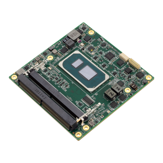
- Page 1 COM-TGUC6 COM Express Module User ’s Manual 1 Last Updated: October 25, 2021...
- Page 2 AAEON assumes no liabilities resulting from errors or omissions in this document, or from the use of the information contained herein. AAEON reserves the right to make changes in the product design without notice to its users.
- Page 3 Acknowledgements All other products’ name or trademarks are properties of their respective owners. Microsoft Windows is a registered trademark of Microsoft Corp. ⚫ Intel® and Celeron® are registered trademarks of Intel Corporation ⚫ Intel Core™ is a trademark of Intel Corporation ⚫...
- Page 4 Packing List Before setting up your product, please make sure the following items have been shipped: I t em Quantity COM-TGUC6 ⚫ If any of these items are missing or damaged, please contact your distributor or sales representative immediately. Preface...
- Page 5 (if any), its specifications, dimensions, jumper/connector settings/definitions, and driver installation instructions (if any), to facilitate users in setting up their product. Users may refer to the product page at AAEON.com for the latest version of this document. Preface...
- Page 6 Saf e ty Precautions Please read the following safety instructions carefully. It is advised that you keep this manual for future references All cautions and warnings on the device should be noted. Make sure the power source matches the power rating of the device. Position the power cord so that people cannot step on it.
- Page 7 If any of the following situations arises, please the contact our service personnel: Damaged power cord or plug Liquid intrusion to the device iii. Exposure to moisture Device is not working as expected or in a manner as described in this manual The device is dropped or damaged Any obvious signs of damage displayed on the device...
- Page 8 FCC Statement This device complies with Part 15 FCC Rules. Operation is subject to the following two conditions: (1) this device may not cause harmful interference, and (2) this device must accept any interference received including interference that may cause undesired operation.
- Page 9 Chi na RoHS Requirements ( CN) 产品中有毒有害物质或元素名称及含量 AAEON Main Board/ Daughter Board/ Backplane 有毒有害物质或元素 部件名称 铅 汞 镉 六价铬 多溴联苯 多溴二苯醚 (Pb) (Hg) (C d) (C r(VI)) (PBB) (PBDE) 印刷电路板 ○ ○ ○ ○ ○ ○ 及其电子组件 外部信号 ○ ○...
- Page 10 Chi na RoHS Requirement (EN) Poisonous or Hazardous Substances or Elements in Products AAEON Main Board/ Daughter Board/ Backplane Poisonous or Hazardous Substances or Elements He xavalent Polybrominated Polybrominated C omponent Le ad Me rcury C admium C hromium Biphenyls...
-
Page 11: Table Of Contents
On-Module H/W Monitor ..............30 3.4.4.1 Smart Fan Mode Configuration ..........31 3.4.5 PCH-FW Configuration..............34 3.4.6.1 Firmware Update Configuration ..........35 3.4.6 On-Module Co nfig uration ..............36 3.4.7 Power Management ................37 3.4.8 AAEON BIOS Robot................38 Setup Submenu: System I/O................ 40 Preface... - Page 12 3.5.1 PCI Express Configuration ..............41 3.5.2 Storage Configuration ............... 44 3.5.3 HD Audio Configuration..............46 3.5.4 Digital IO Port Config uration ............47 3.5.5 Legacy Logical Devices Config uration..........48 3.5.5.1 Serial Port 1 Configuration............49 3.5.5.2 Serial Port 2 Configuration ............50 3.5.6 Serial Port Console Redirection............51 Setup Submenu: Security ................
- Page 13 Preface XIII...
-
Page 14: Chapter 1 - Product Specifications
Chapter 1 Chapter 1 - Product Specifications... -
Page 15: Specifications
1 .1 Spe cifications System F o rm Factor COM Express Compact size, Type 6 CP U 11th Gen Intel® Core™ Series Processor CP U Frequency Up to 1.8 GHz, i7-1185GRE Chip set 11th Gen Intel® Core™ Series Processor Memory Type DDR4 3200 SODIMM x 2 Max. - Page 16 Di splay VGA /LCD Controller Intel® Iris® Xe Graphics/ UHD Graphics Vid eo Output 4 Simultaneous Displays: 18/24-bit 2 Channel LVDS/eDP x 1 (Default: LVDS) DDI x 3 VGA x 1 Et hernet Intel® i225LM, up to 2.5 Gbps Ethernet x 1 A ud io High Definition Audio Interface U SB Port...
-
Page 17: Chapter 2 - Hardware Information
Chapter 2 Chapter 2 – Hardware Information... -
Page 18: Dimensions
Di mensions 8 1 . 5 5 2 . 5 4 0 . 9 6 2 7 . 5 Chapter 2 – Hardware Information... - Page 19 5 . 4 3 2 . 0 0 Wit h COM- TGUC6 - HSP0 1 & COM- FAN0 2 W it h Heat Spreader and Active Cooling (Part No: COM-TGUC6-HSP01 and COM-FAN02) ( 3 7 . 2 ) 1 1 . 0 0 0 .
-
Page 20: Jumpers And Connectors
2.2 Jum pers and Connectors To p Side DDR2 DDR1 B o ttom Side JSP1 1 J RTC1 COMCD1 COMAB1 Chapter 2 – Hardware Information... -
Page 21: List Of Connectors
2.3 Li st of Connectors Please refer to the table below for all of the board’s connectors that you can configure for your application Lab el F unction COMAB1 Express ROW A/B Connector COMCD1 Express ROW C/D Connector DDR 1 DDR4 SO-DIMMCOM Connector DDR 2 DDR4 SO-DIMMCOM Connector... - Page 22 R o w A R o w B P in Sig nal P in Sig nal A 14 B 14 SMB_DAT A 15 SUS_S3# B 15 SMB_ALERT# A 16 SATA0_TX+ B 16 SATA1_TX+ A 17 SATA0_TX- B 17 SATA1_TX- A 18 SUS_S4# B 18 SUS_STAT#...
- Page 23 R o w A R o w B P in Sig nal P in Sig nal A 39 USB4- B 39 USB5- A 40 USB4+ B 40 USB5+ A 41 GND (FIXED) B 41 GND (FIXED) A 42 USB2- B 42 USB3- A 43 USB2+...
- Page 24 R o w A R o w B P in Sig nal P in Sig nal A 64 PCIE_TX1+ B 64 PCIE_RX1+ A 65 PCIE_TX1- B 65 PCIE_RX1- A 66 B 66 WAKE0# A 67 GPI2 B 67 WAKE1# A 68 PCIE_TX0+ B 68 PCIE_RX0+...
- Page 25 R o w A R o w B P in Sig nal P in Sig nal A 89 PCIE_CLK_REF- B 89 VGA_RED A 90 GND (FIXED) B 90 GND (FIXED) A 91 SPI_POWER B 91 VGA_GRN A 92 SPI_MISO B 92 VGA_BLU A 93 GPO0...
-
Page 26: Com Express Row C/D Co Nnector (Cn3)
2.4.2 COM E xpress ROW C/D Connector ( CN3) R o w C R o w D P in Sig nal P in Sig nal GND (FIXED) GND (FIXED) USB_SSRX0- USB_SSTX0- USB_SSRX0+ USB_SSTX0+ USB_SSRX1- USB_SSTX1- USB_SSRX1+ USB_SSTX1+ USB_SSRX2- USB_SSTX2- USB_SSRX2+ USB_SSTX2+ GND (FIXED) GND (FIXED) - Page 27 R o w C R o w D P in Sig nal P in Sig nal DDI1_HPD DDI1_PAIR0+ DDI1_PAIR0- DDI1_PAIR1+ DDI1_PAIR1- GND (FIXED) DDI2_CTRLCLK_AUX+ DDI1_PAIR2+ DDI2_CTRLDATA_AUX- DDI1_PAIR2- DDI2_DDC_AUX_SEL DDI1_DDC_AUX_SEL DDI3_CTRLCLK_AUX+ DDI1_PAIR3+ DDI3_CTRLDATA_AUX- DDI1_PAIR3- DDI3_DDC_AUX_SEL DDI3_PAIR0+ DDI2_PAIR0+ DDI3_PAIR0- DDI2_PAIR0- GND(FIXED) GND (FIXED) DDI3_PAIR1+ DDI2_PAIR1+ DDI3_PAIR1-...
- Page 28 R o w C R o w D P in Sig nal P in Sig nal DDI3_PAIR3+ DDI2_PAIR3+ DDI3_PAIR3- DDI2_PAIR3- GND(FIXED) GND (FIXED) PEG_RX0+ PEG_TX0+ PEG_RX0- PEG_TX0- PEG_LANE_RV# PEG_RX1+ PEG_TX1+ PEG_RX1- PEG_TX1- TYPE2# PEG_RX2+ PEG_TX2+ PEG_RX2- PEG_TX2- GND(FIXED) GND(FIXED) PEG_RX3+ PEG_TX3+ PEG_RX3- PEG_TX3-...
- Page 29 R o w C R o w D P in Sig nal P in Sig nal GND (FIXED) GND (FIXED) GND (FIXED) GND (FIXED) Chapter 2 – Hardware Information...
- Page 30 R o w C R o w D P in Sig nal P in Sig nal C100 GND (FIXED) D100 GND (FIXED) C101 D101 C102 D102 C103 D103 C104 VCC_12V D104 VCC_12V C105 VCC_12V D105 VCC_12V C106 VCC_12V D106 VCC_12V C107 VCC_12V D107...
-
Page 31: Function Block Diagram
2.5 Function Block Diagram Chapter 2 – Hardware Information... -
Page 32: Chapter 3 - Ami Bios Setup
Chapter 3 Chapter 3 - AMI BIOS Setup... -
Page 33: System Test And Initialization
The CMOS memory has lost power and the configuration information has been ⚫ erased. The COM-TGUC6 CMOS memory uses a backup battery for data retention. The battery must be replaced if it runs out of power. Chapter 3 – AMI BIOS Setup... -
Page 34: Ami Bios Setup
3.2 AMI BIOS Setup The AMI BIOS ROM has a built-in Setup program that allows users to modify the basic system configuration. This information is stored in the battery-backed CMOS RAM and BIOS NVRAM so it retains the Setup information when the power is turned off. To enter Setup, power on the computer and press <Del>... -
Page 35: Setup Submenu: Main
3.3 Se tup Submenu: Main Chapter 3 – AMI BIOS Setup... -
Page 36: Setup Submenu: Advanced
3.4 Se tup Submenu: Advanced Chapter 3 – AMI BIOS Setup... -
Page 37: Graphics Configuration
3.4.1 G raphics Configuration Op tions Summary VB T Select LVDS On eDP On eDP/LVDS Off Optimal Default, Failsafe Default Select VBT for GOP Driver Chapter 3 – AMI BIOS Setup... -
Page 38: Lvds Panel Configuration
3.4.1.1 LVDS Panel Configuration Op tions Summary Panel Type 640x480@60Hz 800x480@60Hz 800x600@60Hz 1024x600@60Hz 1024x768@60Hz Optimal Default, Failsafe Default 1280x768@60Hz 1280x800@60Hz 1280x1024@60Hz 1366x768@60Hz 1440x900@60Hz 1600x1200@60Hz 1920x1080@60Hz 1920x1200@60Hz Select panel type Table Continues on Next Page… Chapter 3 – AMI BIOS Setup... - Page 39 Op tions Summary Co lor Depth 18-Bit Optimal Default, Failsafe Default 24-Bit 36-Bit 48-Bit Select panel type B acklight Mode BIOS & Application Windows Slider Optimal Default, Failsafe Default Select backlight control signal type Chapter 3 – AMI BIOS Setup...
-
Page 40: Cpu Configuration
3.4.2 CPU Configuration Op tions Summary A ctive Processor Cores Optimal Default, Failsafe Default Number of cores to enable in each processor package. Turbo Mode Disabled Enabled Optimal Default, Failsafe Default Enable/Disable processor Turbo Mode (requires EMTTM enabled too). AUTO means enabled Hyper-Threading Disabled... - Page 41 Op tions Summary I nt el (VMX) Virtualization Disabled Technology Enabled Optimal Default, Failsafe Default When enabled, a VMM can utilize the additional hardware capabilities provided by Vanderpool Technology. Chapter 3 – AMI BIOS Setup...
-
Page 42: Memory Config Uration
3.4.3 Me mor y Configuration Op tions Summary I n-Band ECC Support Disabled Enabled Optimal Default, Failsafe Default Enable/Disable In-Band ECC. Either the IBECC or the TME can be enabled. I n-Band ECC Error Disabled Optimal Default, Failsafe Default I njection Enabled By enabling this Error Injection feature, the user acknowledges the security risks. -
Page 43: On-Module H/W Monitor
3.4.4 On-Module H/W Monitor Chapter 3 – AMI BIOS Setup... -
Page 44: Smart Fan Mode Configuration
3.4.4.1 Sm ar t Fan Mode Configuration FAN 1: Full Mode Op tions Summary FAN 1 Full Mode Optimal Default, Failsafe Default Manual Mode by PWM Auto Mode by PWM Smart Fan Mode Select P W M signal Non-inverting Optimal Default, Failsafe Default Inverting Select output PWM of inverting or non-inverting signal. - Page 45 FAN 1: Manual Mode by PWM Op tions Summary Manual Setting Optimal Default, Failsafe Default Set Fan at fixed Duty-Cycle Min=0 Max=100 Please input Dec number: Chapter 3 – AMI BIOS Setup...
- Page 46 FAN 1: Auto Mode by PWM Op tions Summary Mo nitor Thermal CPU Temperature (PECI) Optimal Default, Failsafe Default Thermal Source 1(T1) Thermal Source 2(T2) Select monitor thermal source Temperature Of Start Optimal Default, Failsafe Default Temperature Of Start Temperature of Off Optimal Default, Failsafe Default Temperature of Off St art PWM...
-
Page 47: Pch-Fw Configuration
3.4.5 PCH-FW Configuration Chapter 3 – AMI BIOS Setup... -
Page 48: Firmware Update Configuration
3.4.6.1 Fi rmware Update Configuration Op tions Summary Me F W Image Disabled Optimal Default, Failsafe Default R e-Flash Enabled Enable/ Disable Me FW Image Re-Flash Function. F W Update Disabled Enabled Optimal Default, Failsafe Default Enable/Disable ME FW Update Function Chapter 3 –... -
Page 49: On-Module Configuration
3.4.6 On-Module Configuration Op tions Summary B attery Management Disabled Optimal Default, Failsafe Default One Battery Enable to support battery in ACPI OS by I2C_CK, I2C_DAT (B33, B34) EC- SMB-HC Support Disabled Optimal Default, Failsafe Default Enabled SMBus Host Controller Interface via Embedded Controller. Chapter 3 –... -
Page 50: Power Management
3.4.7 Powe r Management Op tions Summary Po wer Mode ATX Type Optimal Default, Failsafe Default AT Type Select system power mode. R estore AC Power Loss Last State Always On Always Off Optimal Default, Failsafe Default SIO Restore AC Power Loss: To decide the behavior after system power cut then resupply. -
Page 51: Aaeon Bios Robot
3.4.8 AAE ON BIOS Robot Op tions Summary Sends watch dog before Disabled Optimal Default, Failsafe Default B I OS POST Enabled Enabled - Robot set Watch Dog Timer (WDT) right after power on, before BIOS start POST process. And then Robot will clear WDT on completion of POST. WDT will reset system automatically if it is not cleared before its timer counts down to zero. - Page 52 Op tions Summary Delayed POST Disabled Optimal Default, Failsafe Default (DX E phase) Enabled Enabled - Robot holds BIOS before POST completion. This allows BIOS POST to start with stable power or start after system is physically warmed-up. N o te: Robot does this after 'Send watch dog before BIOS POST'. R eset system once Disabled Optimal Default, Failsafe Default...
-
Page 53: Setup Submenu: System I/O
3.5 Se tup Submenu: System I/O Chapter 3 – AMI BIOS Setup... -
Page 54: Pci Express Configuration
3.5.1 PCI E xpress Configuration Op tions Summary P CI Express Root Port Disabled Enabled Optimal Default, Failsafe Default Control the PCI Express Root Port. P CI e Speed Auto Optimal Default, Failsafe Default Gen1 Gen2 Gen3 Gen4 Configure PCIe Speed Ho t Plug Disabled Optimal Default, Failsafe Default... - Page 55 Op tions Summary P CI e 0_3 Select PCIE Controller are four ×1 Optimal Default, Failsafe Default PCIE Controller are one ×2 and two ×1 PCIE Controller are two ×2 PCIE Controller is one ×4 PCIE Controller Selection P CI Express 0 Disable Enable Optimal Default, Failsafe Default...
- Page 56 Op tions Summary P CI Express 3 Disable Enable Optimal Default, Failsafe Default Control the PCI Express Root Port. P CI e Speed Auto Optimal Default, Failsafe Default Gen1 Gen2 Gen3 Configure PCIe Speed Ho t Plug Disabled Optimal Default, Failsafe Default Enabled PCI Express Hot Plug Enable/Disable P CI Express 4...
-
Page 57: Storage Configuration
3.5.2 Storage Configuration Op tions Summary SATA Controller(s) Enabled Optimal Default, Failsafe Default Disabled Enable/Disable SATA Device. Po rt 0 Disabled Enabled Optimal Default, Failsafe Default Enable or Disable SATA Port Ho t Plug Disabled Optimal Default, Failsafe Default Enabled Designates this port as Hot Pluggable SATA Device Type Hard Disk Drive... - Page 58 Op tions Summary Ho t Plug Disabled Optimal Default, Failsafe Default Enabled Designates this port as Hot Pluggable SATA Device Type Hard Disk Drive Optimal Default, Failsafe Default Solid State Drive Identify the SATA port is connected to Solid State Drive or Hard Disk Drive Chapter 3 –...
-
Page 59: Hd Audio Configuration
3.5.3 HD Audio Configuration Op tions Summary HD A udio Disabled Enabled Optimal Default, Failsafe Default Control Detection of the HD-Audio device. Disabled = HDA will be unconditionally disabled Enabled = HDA will be unconditionally enabled. Chapter 3 – AMI BIOS Setup... -
Page 60: Digital Io Port Config Uration
3.5.4 Di gital IO Port Configuration Op tions Summary GP I* Input Optimal Default, Failsafe Default Output Set DIO as Input or Output GP O* Input Output Optimal Default, Failsafe Default Set DIO as Input or Output Out put Level High Optimal Default, Failsafe Default Set output level when DIO pin is output... -
Page 61: Legacy Logical Devices Config Uration
3.5.5 Le gacy Logical Devices Configuration Chapter 3 – AMI BIOS Setup... -
Page 62: Serial Port 1 Configuration
3.5.5.1 Se ri al Port 1 Configuration Op tions Summary U s e This Device Disabled Enabled Optimal Default, Failsafe Default Enable or Disable this Logical Device. Po ssible: Use Automatic Settings Optimal Default, Failsafe Default IO=3F8h; IRQ=4; DMA ; IO=2C8h;... -
Page 63: Serial Port 2 Configuration
3.5.5.2 Se ri al Port 2 Configuration Op tions Summary U s e This Device Disabled Enabled Optimal Default, Failsafe Default Enable or Disable this Logical Device. Po ssible: Use Automatic Settings Optimal Default, Failsafe Default IO=2F8h; IRQ=3 DMA ; IO=2D8h;... -
Page 64: Serial Port Console Redirection
3.5.6 Se ri al Port Console Redirection Op tions Summary Co nsole Redirection Disabled Optimal Default, Failsafe Default Enabled Console Redirection Enable or Disable. Chapter 3 – AMI BIOS Setup... -
Page 65: Setup Submenu: Security
3.6 Se tup Submenu: Security Change Administrator/User Password Y ou can set an Administrator password. If you set an Administrator password , you can then set a User password. User passwords do not have access to many of the features in the Setup utility. -
Page 66: Trusted Computing
3.6.1 Trusted Computing Op tions Summary Security Device Disable Optimal Default, Failsafe Default Sup port Enable Enables or Disables BIOS support for security device. O.S. will not show Security Device. TGU EFI protocol and INT1A interface will not be available. SHA-1 PCR Bank Disabled Optimal Default, Failsafe Default... - Page 67 Op tions Summary Pending operation None Optimal Default, Failsafe Default TPM Clear Schedule an Operation for the Security Device. Note: Y our Computer will reboot during restart in order to change State of Security Device. P latform Hierarchy Disabled Enabled Optimal Default, Failsafe Default Enable or Disable Platform Hierarchy St orage Hierarchy...
-
Page 68: Secure Boot
3.6.2 Se cure Boot Op tions Summary Secure Boot Disabled Optimal Default, Failsafe Default Enabled Secure Boot feature is Active if Secure Boot is Enabled, Platform Key (PK) is enrolled and the System is in User mode. The mode change requires platform reset Secure Boot Mode Standard Custom... -
Page 69: Key Management
3.6.1.1 Ke y Management Op tions Summary Factory Key Provision Disabled Optimal Default, Failsafe Default Enabled Install factory default Secure Boot keys after the platform reset and while the System is in Setup mode Chapter 3 – AMI BIOS Setup... -
Page 70: Setup Submenu: Boot
3.7 Se tup Submenu: Boot Op tions Summary Quiet Boot Disabled Enabled Optimal Default, Failsafe Default Enables or Disables Quite Boot option N etwork Stack Disabled Optimal Default, Failsafe Default UEFI Enable/Disable UEFI Network Stack Chapter 3 – AMI BIOS Setup... -
Page 71: Setup Submenu: Save & Exit
3.8 Se tup submenu: Save & Exit Chapter 3 – AMI BIOS Setup... -
Page 72: Chapter 4 - Drivers Installation
Chapter 4 Chapter 4 – Drivers Installation... -
Page 73: Drivers Download And Installation
Dri vers Download and Installation Drivers for the COM-TGUC6 can be downloaded from the product page on the AAEON website by following this link: https://www.aaeon.com/en/p/com-express-cpu-modules-com-tguc6 Download the driver(s) you need and follow the steps below to install them . A ud io Driver (Windows 10) Open the folder where you unzipped the A ud io Drivers Run the Set up.exe in the folder... - Page 74 L A N Drivers (Windows 10) Open the folder where you unzipped the LA N Drivers Read the ReadMe.txt file before proceeding. Caut ion: Be sure to install the driver package before installing the Intel® PROSet package. Open the W ired_driver_26.3_x64 folder Run the W ired_driver_26.3_x64.exe file in the folder Follow the instructions, drivers will be installed automatically.
- Page 75 Peripheral Driver (Linux) Open the folder where you unzipped the P eripheral Drivers Follow the instructions contained within the user guides to install the related drivers. Chapter 4 – Driver Installation...
-
Page 76: Appendix A - Watchdog Timer
Appendix A Appendix A - Watchdog Timer... -
Page 77: Watchdog Timer Initial Program
Watchdog T imer Initial Program Tab le 1: Embedded BRAM relative register table Default Value N o te I nd ex 0x284(Note1) BRAM Index Register Dat a 0x285(Note2) BRAM Data Register Lo g ical Device Number 0xA 8(Note3) Watch dog Logical Device Number F unction and Device Number 0x00(Note4) Watch dog Function/Device Number... - Page 78 ************************************************************************************ // Embedded BRAM relative definition (Please reference to Table 1) #define byte EcBRAMIndex //This parameter is represented from Note1 #define byte EcBRAMData //This parameter is represented from Note2 #define byte BRAMLDNReg //This parameter is represented from Note3 #define byte BRAMFnDataReg //This parameter is represented from Note4 #define void EcBRAMWriteByte(byte Offset, byte Value);...
- Page 79 ************************************************************************************ Main VOID // Procedure : AaeonWDTConfig // (byte)Timer : Time of WDT timer.(0x00~0xFF) // (boolean)Unit : Select time unit(0: second, 1: minute). AaeonWDTConfig(); // Procedure : AaeonWDTEnable // This procudure will enable the WDT counting. AaeonWDTEnable(); ************************************************************************************ Appendix A – Watchdog Timer Programming...
- Page 80 ************************************************************************************ // Procedure : AaeonWDTEnable AaeonWDTEnable () VOID WDTEnableDisable( // Procedure : AaeonWDTConfig AaeonWDTConfig () VOID // Disable WDT counting WDTEnableDisable( // WDT relative parameter setting WDTParameterSetting(); WDTEnableDisable(byte Value) VOID ECBRAMWriteByte(TimerReg , Value); WDTParameterSetting() VOID Byte TempByte; // Watchdog Timer counter setting ECBRAMWriteByte(TimerReg , TimerVal);...
- Page 81 ************************************************************************************ ECBRAMWriteByte(byte OPReg, byte OPBit, byte Value) VOID IOWriteByte(EcBRAMIndex, 0x10); IOWriteByte(EcBRAMData, BRAMLDNReg); IOWriteByte(EcBRAMIndex, 0x11); IOWriteByte(EcBRAMData, BRAMFnDataReg); IOWriteByte(EcBRAMIndex, 0x13 + OPReg); IOWriteByte(EcBRAMData, Value); IOWriteByte(EcBRAMIndex, 0x12); IOWriteByte(EcBRAMData, 0x30); //Write start ECBRAMReadByte(byte OPReg) Byte IOWriteByte(EcBRAMIndex, 0x10); IOWriteByte(EcBRAMData, BRAMLDNReg); IOWriteByte(EcBRAMIndex, 0x11); IOWriteByte(EcBRAMData, BRAMFnDataReg); IOWriteByte(EcBRAMIndex, 0x12); IOWriteByte(EcBRAMData, 0x10);...
-
Page 82: Appendix B - I/O Information
Appendix B Appendix B - I/O Information... -
Page 83: I/O Address Map
I/O Address Map Appendix B – I/O Informati o n... - Page 84 Appendix B – I/O Informati o n...
-
Page 85: Memory Address Map
B.2 Me m or y Address Map Appendix B – I/O Informati o n... -
Page 86: Large Memory Address Map
B.3 Large Memory Address Map Appendix B – I/O Informati o n... -
Page 87: Irq Mapping Chart
B.4 IRQ Mapping Chart Appendix B – I/O Informati o n... - Page 88 Appendix B – I/O Informati o n...
- Page 89 Appendix B – I/O Informati o n...
- Page 90 Appendix B – I/O Informati o n...
- Page 91 Appendix B – I/O Informati o n...
- Page 92 Appendix B – I/O Informati o n...
- Page 93 Appendix B – I/O Informati o n...
- Page 94 Appendix B – I/O Informati o n...
- Page 95 Appendix B – I/O Informati o n...
- Page 96 Appendix B – I/O Informati o n...
- Page 97 Appendix B – I/O Informati o n...
-
Page 98: Appendix C - Programming Digital I/O
Appendix C Appendix C – Programming Digital I/O... -
Page 99: Digital I/O Programming
Di gital I/O Programming The COM-TGUC6 utilizes an AAEON chipset as its Digital I/O controller. Below are the procedures to complete its configuration, which you can use to develop a customized program to fit your application. C.2 Di gital I/O Register... -
Page 100: Digital I/O Sample Program
C.3 Di gital I/O Sample Program ************************************************************************************ // Embedded BRAM relative definition (Please reference to Table 1) #define byte EcBRAMIndex //This parameter is represented from Note1 #define byte EcBRAMData //This parameter is represented from Note2 #define byte BRAMLDNReg //This parameter is represented from Note3 #define byte BRAMFnData0Reg //This parameter is represented from Note4 #define byte BRAMFnData1Reg //This parameter is represented from Note5 #define void EcBRAMWriteByte(byte Offset, byte Value);... - Page 101 ************************************************************************************ Main VOID Boolean PinStatus ; // Procedure : AaeonReadPinStatus // Input : Example, Read Digital I/O Pin 3 status // Output : InputStatus : 0: Digital I/O Pin level is low 1: Digital I/O Pin level is High PinStatus = AaeonReadPinStatus(DIO0ToDIO7Reg, DIO3Bit); // Procedure : AaeonSetOutputLevel // Input : Example, Set Digital I/O Pin 6 level...
- Page 102 ************************************************************************************ AaeonReadPinStatus(byte OptionReg, byte BitNum) Boolean Byte TempByte; TempByte = ECBRAMReadByte(BRAMFnData1Reg, OptionReg); If (TempByte & BitNum == 0) Return 0; Return 1; AaeonSetOutputLevel(byte OptionReg, byte BitNum, byte Value) VOID Byte TempByte; TempByte = ECBRAMReadByte(BRAMFnData1Reg, OptionReg); TempByte |= (Value << BitNum); ECBRAMWriteByte(OptionReg, BitNum, Value);...
- Page 103 ************************************************************************************ ECBRAMWriteByte(byte OPReg, byte OPBit, byte Value) VOID IOWriteByte(EcBRAMIndex, 0x10); IOWriteByte(EcBRAMData, BRAMLDNReg); IOWriteByte(EcBRAMIndex, 0x11); IOWriteByte(EcBRAMData, BRAMFnDataReg); IOWriteByte(EcBRAMIndex, 0x13 + OPReg); IOWriteByte(EcBRAMData, Value); IOWriteByte(EcBRAMIndex, 0x12); IOWriteByte(EcBRAMData, 0x30); //Write start ECBRAMReadByte(byte FnDataReg, byte OPReg) Byte IOWriteByte(EcBRAMIndex, 0x10); IOWriteByte(EcBRAMData, BRAMLDNReg); IOWriteByte(EcBRAMIndex, 0x11); IOWriteByte(EcBRAMData, FnDataReg); IOWriteByte(EcBRAMIndex, 0x12);...
Need help?
Do you have a question about the COM-TGUC6 and is the answer not in the manual?
Questions and answers