
Subscribe to Our Youtube Channel
Related Manuals for Aaeon NanoCOM-KBU-A20


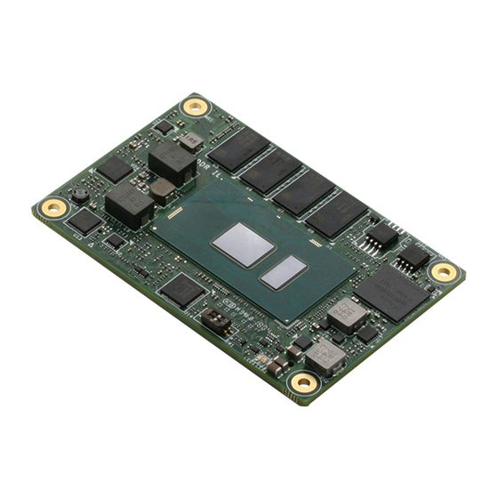
Summary of Contents for Aaeon NanoCOM-KBU-A20
- Page 1 NanoCOM-KBU-A20 COM Express Module User’s Manual 1 Last Updated: March 13, 2019...
- Page 2 The material in this document is for product information only and is subject to change without notice. While reasonable efforts have been made in the preparation of this document to assure its accuracy, AAEON assumes no liabilities resulting from errors or omissions in this document, or from the use of the information contained herein.
- Page 3 Acknowledgement All other products’ name or trademarks are properties of their respective owners. Microsoft Windows is a registered trademark of Microsoft Corp. Intel, Pentium, Celeron, and Xeon are registered trademarks of Intel Corporation Core, Atom are trademarks of Intel Corporation ...
- Page 4 Packing List Before setting up your product, please make sure the following items have been shipped: Item Quantity NanoCOM-KBU-A20 If any of these items are missing or damaged, please contact your distributor or sales representative immediately. Preface...
- Page 5 (if any), its specifications, dimensions, jumper/connector settings/definitions, and driver installation instructions (if any), to facilitate users in setting up their product. Users may refer to the AAEON.com for the latest version of this document. Preface...
- Page 6 Safety Precautions Please read the following safety instructions carefully. It is advised that you keep this manual for future references All cautions and warnings on the device should be noted. Make sure the power source matches the power rating of the device. Position the power cord so that people cannot step on it.
- Page 7 If any of the following situations arises, please the contact our service personnel: Damaged power cord or plug Liquid intrusion to the device iii. Exposure to moisture Device is not working as expected or in a manner as described in this manual The device is dropped or damaged Any obvious signs of damage displayed on the device...
- Page 8 FCC Statement This device complies with Part 15 FCC Rules. Operation is subject to the following two conditions: (1) this device may not cause harmful interference, and (2) this device must accept any interference received including interference that may cause undesired operation.
- Page 9 China RoHS Requirements (CN) 产品中有毒有害物质或元素名称及含量 AAEON Main Board/ Daughter Board/ Backplane 有毒有害物质或元素 部件名称 铅 汞 镉 六价铬 多溴联苯 多溴二苯醚 (Pb) (Hg) (Cd) (Cr(VI)) (PBB) (PBDE) 印刷电路板 × ○ ○ ○ ○ ○ 及其电子组件 外部信号 × ○ ○ ○ ○ ○...
- Page 10 China RoHS Requirement (EN) Poisonous or Hazardous Substances or Elements in Products AAEON Main Board/ Daughter Board/ Backplane Poisonous or Hazardous Substances or Elements Hexavalent Polybrominated Polybrominated Component Lead Mercury Cadmium Chromium Biphenyls Diphenyl Ethers (Pb) (Hg) (Cd) (Cr(VI)) (PBB) (PBDE) PCB &...
-
Page 11: Table Of Contents
Table of Contents Chapter 1 - Product Specifications ..................1 Specifications ........................2 Chapter 2 – Hardware Information ..................5 Dimensions, Jumpers and Connectors ..............6 List of Switches and Connectors ................8 2.2.1 AT/ATX Switch (SW1) ..................9 2.2.2 ROW A/B Connector (CN1) ................9 Chapter 3 - AMI BIOS Setup .................... - Page 12 3.4.9 Trusted Computing ..................36 3.4.10 Firmware Update Configuration ............... 38 3.4.11 SCS Configuration..................39 Chipset ..........................40 3.5.1 System Agent (SA) Configuration ............41 3.5.1.1 Graphics Configuration ............... 42 3.5.1.2 LVDS Panel Configuration ............44 3.5.2 PCH-IO Configuration ................. 46 Security ..........................
- Page 13 Notes for Users – Display Mode ................80 Notes for Users – CPU Support Matrix ..............81 Preface XIII...
-
Page 14: Chapter 1 - Product Specifications
Chapter 1 Chapter 1 - Product Specifications... -
Page 15: Specifications
Specifications System Form Factor COM Express Mini size, Type 10 7th generation Intel® Core™ ULT Series Processor CPU Frequency Up to i7-7600U, 2c/4t, 2.8GHz Chipset Intel® Core™/Celeron® Processor SoC Memory Type Non-ECC DDR4-2133 memory down Max. - Page 16 System Operating Temperature 32°F ~ 140°F (0°C ~ 60°C) -40°F ~ 185°F (-40°C ~ 85°C) Option for NANOCOM-SKU series Storage Temperature -40°F ~ 176°F (-40°C ~ 80°C) Operating Humidity 0% ~ 90% relative humidity, non-condensing MTBF (Hours) 80,000 ...
- Page 17 GPIO 8-bit fTPM Supported Display Display Controller Onboard 7th Gen. intel® Core™ U-Series Processor, GT2-520/510 Video Output LVDS LCD/eDP, DDI x 1 LVDS Interface Supports 18bit and 24bit Single channel eDP Interface Support up to 4-lane eDP ...
-
Page 18: Chapter 2 - Hardware Information
Chapter 2 Chapter 2 – Hardware Information... -
Page 19: Dimensions, Jumpers And Connectors
Dimensions, Jumpers and Connectors Component Side Solder Side Chapter 2 – Hardware Information... - Page 20 With Fan and Heat Spreader With Fan Only (no Heat Spreader) Chapter 2 – Hardware Information...
-
Page 21: List Of Switches And Connectors
List of Switches and Connectors Please refer to the table below for all of the board’s jumpers that you can configure for your application Label Function AT/ ATX switch ROW A/B connector Chapter 2 – Hardware Information... -
Page 22: At/Atx Switch (Sw1)
2.2.1 AT/ATX Switch (SW1) Function 1 (On) AT Mode 1 (Off) ATX Mode (Default) 2 (On) RTC reset 2 (Off) RTC Normal (Default) 2.2.2 ROW A/B Connector (CN1) Row A Row B GND (FIXED) GND (FIXED) GBE0_MDI3- GBE0_ACT# GBE0_MDI3+ LPC_FRAME# GBE0_LINK100# LPC_AD0 GBE0_LINK1000#... - Page 23 Row A Row B SUS_S4# SUS_STAT# SATA0_RX+ SATA1_RX+ SATA0_RX- SATA1_RX- GND (FIXED) GND (FIXED) USB3_RXN0 USB3_TXN0 USB3_RXP0 USB3_TXP0 SUS_S5# PWR_OK USB3_RXN1 USB3_TXN1 USB3_RXP1 USB3_TXP1 BATLOW# ATA_ACT# AC_SYNC AC_SDIN1 AC_RST# AC_SDIN0 GND (FIXED) GND (FIXED) AC_BITCLK SPKR AC_SDOUT I2C_CK BIOS_DIS0# I2C_DAT THRMTRIP# THRM# USB6-...
- Page 24 Row A Row B USB0- USB1- USB0+ USB1+ VCC_RTC EXCD1_PERST# EXCD0_PERST# EXCD1_CPPE# EXCD0_CPPE# SYS_RESET# LPC_SERIRQ CB_RESET# GND (FIXED) GND (FIXED) GPI0 GPO1 GPO2 PCIE_TX3+ PCIE_RX3+ PCIE_TX3- PCIE_RX3- GND (FIXED) GND (FIXED) PCIE_TX2+ PCIE_RX2+ PCIE_TX2- PCIE_RX2- GPI1 GPO3 PCIE_TX1+ PCIE_RX1+ PCIE_TX1- PCIE_RX1- WAKE0# GPI2...
- Page 25 Row A Row B LVDS_A0- DDI0_PAIR0- LVDS_A1+ DDI0_PAIR1+ LVDS_A1- DDI0_PAIR1- LVDS_A2+ DDI0_PAIR2+ LVDS_A2- DDI0_PAIR2- LVDS_VDD_EN LVDS_A3+ LVDS_A3- LVDS_BKLD_EN GND (FIXED) GND (FIXED) LVDS_A_CK+ DDI0_PAIR3+ LVDS_A_CK- DDI0_PAIR3- LVDS_I2C_CK LVDS_BKLT_CTRL LVDS_I2C_DAT VCC_5V_SBY GPI3 VCC_5V_SBY VCC_5V_SBY VCC_5V_SBY PCIE0_CK_REF+ BISO_DIS1# PCIE0_CK_REF- DDI0_HPD GND (FIXED) GND (FIXED) SPI_POWER SPI_MISO...
- Page 26 Row A Row B RS1_RX DDI0_CTRL_DATA A100 GND (FIXED) B100 GND (FIXED) A101 RS2_TX B101 FAN_PWMOUT A102 RS2_RX B102 FAN_TACHIN A103 LID# B103 SLEEP# A104 VCC_12V B104 VCC_12V A105 VCC_12V B105 VCC_12V A106 VCC_12V B106 VCC_12V A107 VCC_12V B107 VCC_12V A108 VCC_12V B108...
-
Page 27: Chapter 3 - Ami Bios Setup
Chapter 3 Chapter 3 - AMI BIOS Setup... -
Page 28: System Test And Initialization
4. The CMOS memory has lost power and the configuration information has been erased. The NanoCOM-KBU-A20 CMOS memory has an integral lithium battery backup for data retention. However, you will need to replace the complete unit when it finally runs down. -
Page 29: Ami Bios Setup
AMI BIOS Setup AMI BIOS ROM has a built-in Setup program that allows users to modify the basic system configuration. This type of information is stored in battery-backed CMOS RAM and BIOS NVRAM so that it retains the Setup information when the power is turned off. 3.2.1 Entering Setup Power on the computer and press <Del>or <ESC>... -
Page 30: Main
Main Chapter 3 – AMI BIOS Setup... -
Page 31: Advanced
Advanced Chapter 3 – AMI BIOS Setup... -
Page 32: Cpu Configuration
3.4.1 CPU Configuration Options Summary Hyper-Threading Disabled Enabled Optimal Default, Failsafe Default Enabled for Windows XP and Linux (OS optimized for Hyper-Threading Technology) and Disabled for other OS (OS not optimized for Hyper-Threading Technology). Intel (VMX) Disabled Virtualization Enabled Optimal Default, Failsafe Default Technology When enabled, a VMM can utilize the additional hardware capabilities provided by Vanderpool Technology. -
Page 33: Sata Configuration
3.4.2 SATA Configuration Options Summary SATA Controller(s) Enabled Optimal Default, Failsafe Default Disabled Enable/Disable SATA Device. SATA Controller Disabled Optimal Default, Failsafe Default Speed Gen1 Gen2 Gen3 Indicates the maximum speed the SATA controller can support. Port 0 Disabled Enabled Optimal Default, Failsafe Default Enable or Disable SATA Port. - Page 34 Hot Plug Disabled Optimal Default, Failsafe Default Enabled Designates this port as Hot Pluggable. Port 1 Disabled Enabled Optimal Default, Failsafe Default Enable or Disable SATA Port. Hot Plug Disabled Optimal Default, Failsafe Default Enabled Designates this port as Hot Pluggable. Chapter 3 –...
-
Page 35: Usb Configuration
3.4.3 USB Configuration Options Summary Legacy USB Support Enabled Optimal Default, Failsafe Default Disabled Auto Enables Legacy USB Support. AUTO option disables legacy support if no USB devices are connected. DISABLE option will keep USB device available only for EFI applications. Chapter 3 –... -
Page 36: On-Module Features
3.4.4 On-Module FEATURES Options Summary Battery Disabled Optimal Default, Failsafe Default Managerment One Battery Enable to support battery in ACPI OS by I2C_CK,I2C_DAT(B33,B34) Chapter 3 – AMI BIOS Setup... -
Page 37: Sio Configuration
3.4.5 SIO Configuration Chapter 3 – AMI BIOS Setup... -
Page 38: Sio Configuration: Serial Port 9 Configuration
3.4.5.1 SIO Configuration: Serial Port 9 Configuration Options Summary Use This Device Disabled Enabled Optimal Default, Failsafe Default Enable or Disable this Logical Device. Possible: Use Automatic Settings Optimal Default, Failsafe Default IO=2D8; IRQ=11; DMA; IO=2C8; IRQ=11; DMA; Allows the user to change the device resource settings. New settings will be reflected on this setup page after system restarts. -
Page 39: Sio Configuration: Serial Port 10 Configuration
3.4.5.2 SIO Configuration: Serial Port 10 Configuration Options Summary Use This Device Disabled Enabled Optimal Default, Failsafe Default Enable or Disable this Logical Device. Possible: Use Automatic Settings Optimal Default, Failsafe Default IO=2C8; IRQ=10; DMA; IO=2D8; IRQ=10; DMA; Allows the user to change the device resource settings. New settings will be reflected on this setup page after system restarts. -
Page 40: Power Management
3.4.6 Power Management Options Summary Power Mode ATX Type Optimal Default, Failsafe Default AT Type Select system power mode. Restore AC Power Last State Loss Always On Always Off Optimal Default, Failsafe Default Wake on LAN Enabled Enable Disabled Optimal Default, Failsafe Default Enabled/ Disabled integrated LAN to wake the system. - Page 41 Fixed Time: System will wake on the hr::min::sec specified. Dynameic time: System will wake on the current time + Increase minute(s) Chapter 3 – AMI BIOS Setup...
-
Page 42: Digital Io Port Configuration
3.4.7 Digital IO Port Configuration Options Summary GPI * Input Optimal Default, Failsafe Default Output Set DIO as Input or Output Interrupt Disabled Optimal Default, Failsafe Default Enabled Enabled interrupt function with low pulse mode. This triggered pulse needs more then the 10ms. - Page 43 Set output level when DIO pin is output Chapter 3 – AMI BIOS Setup...
-
Page 44: On Module Hardware Monitor
3.4.8 On Module Hardware Monitor Chapter 3 – AMI BIOS Setup... -
Page 45: Fan 1 Mode Configuration
3.4.8.1 Fan 1 Mode Configuration Options Summary CPU Smart Fan Full Mode Optimal Default, Failsafe Default Mode Manual Mode by PWM Auto Mode by PWM Smart Fan Mode Select PWM signal Non-inverting Optimal Default, Failsafe Default Inverting Select output PWM of inverting or non-uninverting signal Chapter 3 –... -
Page 46: Cpu Smart Fan Mode: Manual Mode By Pwm
3.4.8.2 CPU Smart Fan Mode: Manual Mode by PWM Options Summary Manual Setting Optimal Default, Failsafe Default Set Fan at fixed Duty-Cycle Min=. Max=100 Please input Dec number: Chapter 3 – AMI BIOS Setup... -
Page 47: Cpu Smart Fan Mode : Auto Mode By Pwm
3.4.8.3 CPU Smart Fan Mode : Auto Mode by PWM Options summary: Options Summary Monitor Thermal CPU Temperature(DTS) Optimal Default, Failsafe Default Thermal Source 1(T1) Thermal Source 2(T2) Select monitor thermal source Temperature of Optimal Default, Failsafe Default Start Temperature Of Start Temperature Of Off 20 Optimal Default, Failsafe Default Temperature Of Off... - Page 48 Slope (PWM) 0 (PWM) 1 (PWM) Optimal Default, Failsafe Default 2 (PWM) 4 (PWM) 8 (PWM) 16 (PWM) 32 (PWM) 64 (PWM) Slope (PWM) Chapter 3 – AMI BIOS Setup...
-
Page 49: Trusted Computing
3.4.9 Trusted Computing Options Summary Security Device Disable Support Enable Optimal Default, Failsafe Default Enables or Disables BIOS support for security device. O.S. will not show Security Device. TCG EFI protocol and INT1A interface will not be available. SHA-1 PCR Bank Disable Enable Optimal Default, Failsafe Default... - Page 50 Enable or Disable SHA256 PCR Bank Pending operation None Optimal Default, Failsafe Default TPM Clear Schedule an Operation for the Security Device. NOTE: Your Computer will reboot during restart in order to change state of Security Device. Platform Hierarchy Disable Enable Optimal Default, Failsafe Default Enable or Disable Platform Hierarchy...
-
Page 51: Firmware Update Configuration
3.4.10 Firmware Update Configuration Options summary: Options Summary Me FW Image Disable Optimal Default, Failsafe Default Re-Flash Enable Enable/ Disable Me FW Image Re-Flash functinn. Chapter 3 – AMI BIOS Setup... -
Page 52: Scs Configuration
3.4.11 SCS Configuration Options Summary Emmc 5.0 Controller Disable Enable Optimal Default, Failsafe Default Enable or Disable Emmc 5.0 Controller Chapter 3 – AMI BIOS Setup... -
Page 53: Chipset
Chipset Chapter 3 – AMI BIOS Setup... -
Page 54: System Agent (Sa) Configuration
3.5.1 System Agent (SA) Configuration Chapter 3 – AMI BIOS Setup... -
Page 55: Graphics Configuration
3.5.1.1 Graphics Configuration Options Summary Primary Display Auto Optimal Default, Failsafe Default IGFX Select which of IGFX/PEG/PCI Graphics device should be Primary Display Or select SG for Switchable Gfx. Primary IGFX Boot VBIOS Default Optimal Default, Failsafe Default Display Display Port LVDS Chapter 3 –... - Page 56 Select the Video Device which will be activated during POST. This has no effect if external graphic present. Secondary boot display selection will appear based on your selection. VGA modes will be supported only on primary display Chapter 3 – AMI BIOS Setup...
-
Page 57: Lvds Panel Configuration
3.5.1.2 LVDS Panel Configuration Options Summary LVDS Disabled Enabled Optimal Default, Failsafe Default Enabled/ Disabled this panel Panel Type 640x480@60Hz 800x480@60Hz 800x600@60Hz 1024x600@60Hz 1024x768@60Hz Optimal Default, Failsafe Default 1280x768@60Hz 1280x800@60Hz 1366x768@60Hz Chapter 3 – AMI BIOS Setup... - Page 58 Select panel type Color Depth 18-bit Optimal Default, Failsafe Default 24-bit Select panel type Backlight Type Normal Optimal Default, Failsafe Default Inverted Select backlight control signal type Backlight Level Optimal Default, Failsafe Default 100% Select backlight control level Backlight PWM Freq 100Hz 200Hz 220Hz...
-
Page 59: Pch-Io Configuration
3.5.2 PCH-IO Configuration Options Summary HD Audio Disabled Enabled Auto Optimal Default, Failsafe Default Control Detection of the HD-Audio device. Disabled = HDA will be unconditionally disabled Enabled = HDA will be unconditionally enabled Auto = HDA will be enabled if present, disabled otherwise. PCH LAN Enabled Optimal Default, Failsafe Default... - Page 60 PCIe Configuration PCIE Port1~4 are four x1 Select PCIE Port1~4 is one x4 Optimal Default, Failsafe Default PCIE Port1~4 Selection PCI Express Root Disabled Port 1 Enabled Optimal Default, Failsafe Default Control the PCI Express Root Port. PCIe Speed Auto Gen1 Optimal Default, Failsafe Default Gen2...
-
Page 61: Security
Security Change User/Supervisor Password You can install a Supervisor password, and if you install a supervisor password, you can then install a user password. A user password does not provide access to many of the features in the Setup utility. If you highlight these items and press Enter, a dialog box appears which lets you enter a password. -
Page 62: Secure Boot
3.6.1 Secure Boot Options Summary Attempt Secure Boot Disabled Optimal Default, Failsafe Default Enabled Secure Boot activated when Platform Key(PK) is enrolled, System mode is User/Deployed, and CSM function is disable Secure Boot Mode Standard Custom Optimal Default, Failsafe Default Secure Boot Mode selector: Standard/Custom. -
Page 63: Key Management
3.6.1.1 Key Management Options Summary Provision Factory Disabled Optimal Default, Failsafe Default Defaults Enabled Allow to provision factory default Secure Boot keys when System is in setup Mode Install Factory Default keys Force System to User Mode - install all Factory Default keys Enroll Efi Image Allow the image to run in Secure Boot mode. - Page 64 Platform Key(PK) Enroll Factory Defaults or load certificates from a file: 1.Public Key Certificate in: a)EFI_SIGNATURE_LIST b)EFI_CERT_X509 (DER encoded) c)EFI_CERT_RSA2048 (bin) d)EFI_CERT_SHA256,384,512 2.Authenticated UEFI Variable 3.EFI PE/COFF Image(SHA256) Key Source: Default,External,Mixed,Test Key Exchange Keys Enroll Factory Defaults or load certificates from a file: 1.Public Key Certificate in: a)EFI_SIGNATURE_LIST b)EFI_CERT_X509 (DER encoded)
- Page 65 Authorized Signatures Enroll Factory Defaults or load certificates from a file: 1.Public Key Certificate in: a)EFI_SIGNATURE_LIST b)EFI_CERT_X509 (DER encoded) c)EFI_CERT_RSA2048 (bin) d)EFI_CERT_SHA256,384,512 2.Authenticated UEFI Variable 3.EFI PE/COFF Image(SHA256) Key Source: Default,External,Mixed,Test Forbidden Signatures Enroll Factory Defaults or load certificates from a file: 1.Public Key Certificate in: a)EFI_SIGNATURE_LIST b)EFI_CERT_X509 (DER encoded)
- Page 66 Authorized TimeStamps Enroll Factory Defaults or load certificates from a file: 1.Public Key Certificate in: a)EFI_SIGNATURE_LIST b)EFI_CERT_X509 (DER encoded) c)EFI_CERT_RSA2048 (bin) d)EFI_CERT_SHA256,384,512 2.Authenticated UEFI Variable 3.EFI PE/COFF Image(SHA256) Key Source: Default,External,Mixed,Test OsRecovery Signatures Enroll Factory Defaults or load certificates from a file: 1.Public Key Certificate in: a)EFI_SIGNATURE_LIST b)EFI_CERT_X509 (DER encoded)
-
Page 67: Boot
Boot Options Summary Quiet Boot Disabled Enabled Optimal Default, Failsafe Default Enabled or Disable showing boot logo. Launch PXE OpROM Do not launch Optimal Default, Failsafe Default UEFI UEGI and Legacy Controls the execution of UEFI and Legacy PXE OpROm BIOS MODE UEFI only Optimal Default, Failsafe Default... -
Page 68: Boot: Bbs Priorities
3.7.1 Boot: BBS Priorities Chapter 3 – AMI BIOS Setup... -
Page 69: Save & Exit
Save & Exit Chapter 3 – AMI BIOS Setup... -
Page 70: Chapter 4 - Drivers Installation
Chapter 4 Chapter 4 – Drivers Installation... -
Page 71: Driver Download And Installation
Driver Download and Installation Drivers for the NanoCOM-KBU-A20 can be downloaded from the product page on the AAEON website by following this link: https://www.aaeon.com/en/p/com-express-modules-nanocom-kbu-a20 Download the driver(s) you need and follow the steps below to install them. Step 1 – Install Chipset Drivers Open the Step1 –... - Page 72 Step 5 – Install ME Drivers Open the Step5 - ME folder followed by Setup.exe Follow the instructions Drivers will be installed automatically Step 6 – Install Serial IO Drivers (Windows 10) Open the Step6 – Serial IO folder followed by the Win10_x64 folder Run Setup.exe Follow the instructions Drivers will be installed automatically...
-
Page 73: Appendix A - Watchdog Timer Programming
Appendix A Appendix A - Watchdog Timer Programming... -
Page 74: Watchdog Timer Initial Program
Watchdog Timer Initial Program Table 1 : Embedded BRAM relative register table Default Value Note Index 0x284(Note1) BRAM Index Register Data 0x285(Note2) BRAM Data Register Logical Device Number 0xA8(Note3) Watch dog Logical Device Number Function and Device Number 0x00(Note4) Watch dog Function/Device Number Table 2 : Watchdog relative register table Option BitNum... - Page 75 ************************************************************************************ // Embedded BRAM relative definition (Please reference to Table 1) #define byte EcBRAMIndex //This parameter is represented from Note1 #define byte EcBRAMData //This parameter is represented from Note2 #define byte BRAMLDNReg //This parameter is represented from Note3 #define byte BRAMFnDataReg //This parameter is represented from Note4 #define void EcBRAMWriteByte(byte Offset, byte Value);...
- Page 76 ************************************************************************************ Main VOID // Procedure : AaeonWDTConfig // (byte)Timer : Time of WDT timer.(0x00~0xFF) // (boolean)Unit : Select time unit(0: second, 1: minute). AaeonWDTConfig(); // Procedure : AaeonWDTEnable // This procudure will enable the WDT counting. AaeonWDTEnable(); ************************************************************************************ Appendix A – Watchdog Timer Programming...
- Page 77 ************************************************************************************ // Procedure : AaeonWDTEnable AaeonWDTEnable () VOID WDTEnableDisable( // Procedure : AaeonWDTConfig AaeonWDTConfig () VOID // Disable WDT counting WDTEnableDisable( // WDT relative parameter setting WDTParameterSetting(); WDTEnableDisable(byte Value) VOID ECBRAMWriteByte(TimerReg , Value); WDTParameterSetting() VOID Byte TempByte; // Watchdog Timer counter setting ECBRAMWriteByte(TimerReg , TimerVal);...
- Page 78 ************************************************************************************ ECBRAMWriteByte(byte OPReg, byte OPBit, byte Value) VOID IOWriteByte(EcBRAMIndex, 0x10); IOWriteByte(EcBRAMData, BRAMLDNReg); IOWriteByte(EcBRAMIndex, 0x11); IOWriteByte(EcBRAMData, BRAMFnDataReg); IOWriteByte(EcBRAMIndex, 0x13 + OPReg); IOWriteByte(EcBRAMData, Value); IOWriteByte(EcBRAMIndex, 0x12); IOWriteByte(EcBRAMData, 0x30); //Write start ECBRAMReadByte(byte OPReg) Byte IOWriteByte(EcBRAMIndex, 0x10); IOWriteByte(EcBRAMData, BRAMLDNReg); IOWriteByte(EcBRAMIndex, 0x11); IOWriteByte(EcBRAMData, BRAMFnDataReg); IOWriteByte(EcBRAMIndex, 0x12); IOWriteByte(EcBRAMData, 0x10);...
-
Page 79: Appendix B - I/O Information
Appendix B Appendix B - I/O Information... -
Page 80: I/O Address Map
I/O Address Map Appendix B – I/O Information... -
Page 81: Memory Address Map
Memory Address Map Appendix B – I/O Information... -
Page 82: Irq Mapping Chart
IRQ Mapping Chart Appendix B – I/O Information... -
Page 83: Appendix C - Programming Digital I/O
Appendix C Appendix C – Programming Digital I/O... -
Page 84: Digital I/O Programming
Digital I/O Programming NanoCOM-KBU-A20 utilizes AAEON chipset as its Digital I/O controller. Below are the procedures to complete its configuration which you can develop customized program to fit your application. Appendix C – Programming Digital I/O... -
Page 85: Digital I/O Register
C.2 Digital I/O Register Table 1 : Embedded BRAM relative register table Default Value Note Index 0x284(Note1) BRAM Index Register Data 0x285(Note2) BRAM Data Register Logical Device Number 0xA2(Note3) Watch dog Logical Device Number IO Direction DIO Input/Output Function/Device Function and Device 0x00(Note4) Number Number... - Page 86 Table 2 : Digital I/O relative register table Register Option Register BitNum Value Note GPI0 Pin Status 0x00(Note6) 0(Note7) (Note15) GPA2 GPI1 Pin Status 0x00(Note6) 1(Note8) (Note16) GPA3 GPI2 Pin Status 0x00(Note6) 2(Note9) (Note17) GPA4 GPI3 Pin Status 0x00(Note6) 3(Note10) (Note18) GPA5 GPO0 Pin Status...
-
Page 87: Digital I/O Sample Program
C.3 Digital I/O Sample Program ************************************************************************************ // Embedded BRAM relative definition (Please reference to Table 1) #define byte EcBRAMIndex //This parameter is represented from Note1 #define byte EcBRAMData //This parameter is represented from Note2 #define byte BRAMLDNReg //This parameter is represented from Note3 #define byte BRAMFnData0Reg //This parameter is represented from Note4 #define byte... - Page 88 ************************************************************************************ Main VOID Boolean PinStatus ; // Procedure : AaeonReadPinStatus // Input : Example, Read Digital I/O Pin 3 status // Output : InputStatus : 0: Digital I/O Pin level is low 1: Digital I/O Pin level is High PinStatus = AaeonReadPinStatus(DIO0ToDIO7Reg, DIO3Bit); // Procedure : AaeonSetOutputLevel // Input : Example, Set Digital I/O Pin 6 level...
- Page 89 ************************************************************************************ AaeonReadPinStatus(byte OptionReg, byte BitNum) Boolean Byte TempByte; TempByte = ECBRAMReadByte(BRAMFnData1Reg, OptionReg); If (TempByte & BitNum == 0) Return 0; Return 1; AaeonSetOutputLevel(byte OptionReg, byte BitNum, byte Value) VOID Byte TempByte; TempByte = ECBRAMReadByte(BRAMFnData1Reg, OptionReg); TempByte |= (Value << BitNum); ECBRAMWriteByte(OptionReg, BitNum, Value);...
- Page 90 ************************************************************************************ ECBRAMWriteByte(byte OPReg, byte OPBit, byte Value) VOID IOWriteByte(EcBRAMIndex, 0x10); IOWriteByte(EcBRAMData, BRAMLDNReg); IOWriteByte(EcBRAMIndex, 0x11); IOWriteByte(EcBRAMData, BRAMFnDataReg); IOWriteByte(EcBRAMIndex, 0x13 + OPReg); IOWriteByte(EcBRAMData, Value); IOWriteByte(EcBRAMIndex, 0x12); IOWriteByte(EcBRAMData, 0x30); //Write start ECBRAMReadByte(byte FnDataReg, byte OPReg) Byte IOWriteByte(EcBRAMIndex, 0x10); IOWriteByte(EcBRAMData, BRAMLDNReg); IOWriteByte(EcBRAMIndex, 0x11); IOWriteByte(EcBRAMData, FnDataReg); IOWriteByte(EcBRAMIndex, 0x12);...
-
Page 91: Appendix D - Note For Users
Appendix D Appendix D – Note for Users... -
Page 92: Notes For Users - Hsio Configurations
Config 1 Config 2* PCIe No. (Default) (Custom BIOS only) PCIe#0 PCIe[x1] PCIe#1 PCIe[x1] PCIe[x4] PCIe#2 PCIe[x1] PCIe#3 PCIe[x1] SATA#0 SATA#0 SATA#0 SATA#1 SATA#1 SATA#1 *Config 2 can be requested through your AAEON contact. Appendix D – Note for Users... - Page 93 Legacy Single Display only, default is DP via DDI0. 2 display ok *NANOCOM-KBU-A20 supports either LVDS + DDI0 (DP/HDMI) or option for eDP + DDI0 (DP/HDMI) **Please reach your AAEON contact for eDP support Appendix D – Note for Users...
- Page 94 CPU support: NanoCOM-SKU-A20-xx-xxxxx This product supports: i7-6600U, i5-6300U, i3-6100U, and Celeron 3955U NanoCOM-KBU-A20-xx-xxxxx This product supports: i7-7600U, i5-7300U, i3-7100U, and Celeron 3965U Appendix D – Note for Users...
Need help?
Do you have a question about the NanoCOM-KBU-A20 and is the answer not in the manual?
Questions and answers