Table of Contents

Related Manuals for Aaeon COM-KB


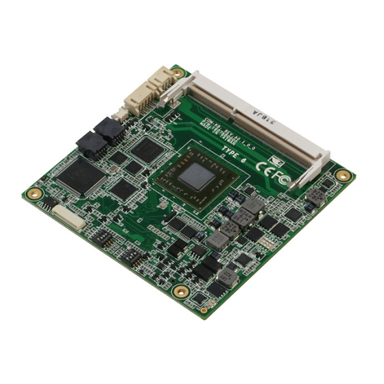
Summary of Contents for Aaeon COM-KB
- Page 1 COM-KB COM Express Module User’s Manual 2 Last Updated: July 26, 2016...
- Page 2 AAEON assumes no liabilities resulting from errors or omissions in this document, or from the use of the information contained herein. AAEON reserves the right to make changes in the product design without notice to its users.
- Page 3 Acknowledgement All other products’ name or trademarks are properties of their respective owners. Microsoft Windows is a registered trademark of Microsoft Corp. Intel, Pentium, Celeron, and Xeon are registered trademarks of Intel Corporation Core, Atom are trademarks of Intel Corporation ...
- Page 4 Packing List Before setting up your product, please make sure the following items have been shipped: Item Quantity COM-KB M2.5 screws Product DVD with User’s Manual (in pdf) and drivers If any of these items are missing or damaged, please contact your distributor or sales representative immediately.
- Page 5 (if any), its specifications, dimensions, jumper/connector settings/definitions, and driver installation instructions (if any), to facilitate users in setting up their product. Users may refer to the AAEON.com for the latest version of this document. Preface...
- Page 6 Safety Precautions Please read the following safety instructions carefully. It is advised that you keep this manual for future references All cautions and warnings on the device should be noted. Make sure the power source matches the power rating of the device. Position the power cord so that people cannot step on it.
- Page 7 If any of the following situations arises, please the contact our service personnel: Damaged power cord or plug Liquid intrusion to the device iii. Exposure to moisture Device is not working as expected or in a manner as described in this manual The device is dropped or damaged Any obvious signs of damage displayed on the device...
- Page 8 FCC Statement This device complies with Part 15 FCC Rules. Operation is subject to the following two conditions: (1) this device may not cause harmful interference, and (2) this device must accept any interference received including interference that may cause undesired operation.
- Page 9 China RoHS Requirements (CN) 产品中有毒有害物质或元素名称及含量 AAEON Main Board/ Daughter Board/ Backplane 有毒有害物质或元素 部件名称 铅 汞 镉 六价铬 多溴联苯 多溴二苯醚 (Pb) (Hg) (Cd) (Cr(VI)) (PBB) (PBDE) 印刷电路板 ○ ○ ○ ○ ○ ○ 及其电子组件 外部信号 ○ ○ ○ ○ ○ ○...
- Page 10 China RoHS Requirement (EN) Poisonous or Hazardous Substances or Elements in Products AAEON Main Board/ Daughter Board/ Backplane Poisonous or Hazardous Substances or Elements Hexavalent Polybrominated Polybrominated Component Lead Mercury Cadmium Chromium Biphenyls Diphenyl Ethers (Pb) (Hg) (Cd) (Cr(VI)) (PBB) (PBDE) PCB &...
-
Page 11: Table Of Contents
Table of Contents Chapter 1 - Product Specifications ..................1 Specifications ......................2 Chapter 2 – Hardware Information ..................4 Dimensions, Jumpers and Connectors ............... 5 List of Jumpers ......................7 2.2.1 DP0 (DDI1) Selection/DP1 (DDI2) Selection (SW1) ........7 2.2.2 Power Type Selection/RTC Clear/DDR3 Voltage Selection/LVDS Backlight Selection (SW2) ................ - Page 12 3.4.3 Advanced: IDE Configuration ..............29 3.4.4 Advanced: USB Configuration ..............30 3.4.5 Advanced: Dynamic Digital IO ..............32 3.4.6 Advanced: Power Management..............33 3.4.6.1 Power Management: S5 RTC Wake Settings (Fixed Time) ..34 3.4.6.2 Power Management: S5 RTC Wake Settings (Dynamic Time) ... 35 3.4.7 Advanced: On-Module IO Configuration ..........
- Page 13 Appendix B - I/O Information ....................66 I/O Address Map ....................67 Memory Address Map ..................69 IRQ Mapping Chart ....................70 Appendix C – Programming Digital I/O................72 Digital I/O Register ....................73 Digital I/O Sample Program ................74 Preface XIII...
-
Page 14: Chapter 1 - Product Specifications
Chapter 1 Chapter 1 - Product Specifications... -
Page 15: Specifications
Specifications System COM Express Basic module, Pin-out Type 6, Form Factor COM. 0 Rev. 2.1 AMD Embedded G-series SoC APU Quad (2 GHz), Dual (1.6 GHz) CPU Frequency AMD® Embedded G-Series SoC Chipset AMD GX-420CA SoC with AMD Radeon™ HD 8400E Graphics(Quad) GX-217GA SoC with AMD Radeon™... - Page 16 -40 ~ 80°C (-40 ~ 176°F) Storage Temperature 0 ~ 90% relative humidity, non-condensing Operation Humidity MTBF 80,000 Certification CE/FCC Class A Display VGA/LCD Controller AMD® eKabini integrated CRT, 24-bit dual channel LVDS (24 x 2), Video Output ...
-
Page 17: Chapter 2 - Hardware Information
Chapter 2 Chapter 2 – Hardware Information... -
Page 18: Dimensions, Jumpers And Connectors
Dimensions, Jumpers and Connectors Component Side Chapter 2 – Hardware Information... - Page 19 Solder Side Chapter 2 – Hardware Information...
-
Page 20: List Of Jumpers
List of Jumpers Please refer to the table below for all of the board’s jumpers that you can configure for your application Label Function DP0 selection/DP1 selection Power type selection/RTC Clear/DDR3 Voltage 2.2.1 DP0 (DDI1) Selection/DP1 (DDI2) Selection (SW1) Function HDMI/DVI 18 bit Single CH LVDS Function... -
Page 21: Power Type Selection/Rtc Clear/Ddr3 Voltage Selection/Lvds
2.2.2 Power Type Selection/RTC Clear/DDR3 Voltage Selection/LVDS Backlight Selection (SW2) Function 1 On ATX (Default) 1 Off 2 On RTC Clear 2 Off RTC reserved (Default) 3 On DDR3 +1.35V (Default) 3 Off DDR3 +1.5V 4 On 18BIT LVDS PWM Control Backlight 4 Off 18BIT LVDS Voltage Control Backlight (Default) Chapter 2 –... -
Page 22: List Of Connectors
List of Connectors Label Function AMD Debug Connector FAN Connector SPI BIOS Program Connector Battery Connector EDP/LVDS Connector LVDS Backlight Connector LPC Connector SPI EC Program Connector ROW_AB Connector CN10 ROW_CD Connector DIMM1 DDR3 SODIMM Connector 2.3.1 AMD Debug Connector (CN1) Reserved for advanced debug 2.3.2 FAN connector (CN2) Signal... -
Page 23: Spi Bios Program Connector (Cn3)
2.3.3 SPI BIOS Program connector (CN3) Signal SPI_DATAIN_F SPI_CLK_F +3V3_SPI SPI_DATAOUT_F SPI_CS#_F 2.3.4 Battery Connector (CN4) Signal +3V From battery 2.3.5 EDP/18BIT LVDS Connector (CN5) Signal +3.3V with Fuse +3.3V with Fuse EDP_TX2_N (18BIT LVDS: L0N) EDP_TX2_P (18BIT LVDS: L0P) Chapter 2 –... -
Page 24: 18Bit Lvds Connector (Cn6)
EDP_TX1_N (18BIT LVDS: L1N) EDP_TX1_P (18BIT LVDS: L1P) EDP_TX0_N (18BIT LVDS: L2N) EDP_TX0_P (18BIT LVDS: L2P) EDP_TX3_N (18BIT LVDS: CLKN) EDP_TX3_P (18BIT LVDS: CLKP) EDP_AUX_N (18BIT LVDS: NC) EDP_AUX_P (18BIT LVDS: NC) VOL_CON BLON EDP_HPD +12V with Fuse +12V with Fuse +12V with Fuse +12V with Fuse 2.3.6 18BIT LVDS Connector (CN6) -
Page 25: Lpc Connector (Cn7)
VOL_PWM (SW2 POS 4) BLON 2.3.7 LPC Connector (CN7) Signal LPC AD0 LPC AD1 LPC AD2 LPC AD3 +3.3V LPC FRAME# LPC_RST# LPC CLK1 LPC DRQ0 SERIRQ 2.3.8 SPI EC Program connector (CN8) Signal FMISO_F FSCK_F +3V3_EC Chapter 2 – Hardware Information... -
Page 26: Row_Ab Connector (Cn9)
FMOSI_F FSCE#_F 2.3.9 ROW_AB connector (CN9) Row A Type 6 Rev. 2.1 Row B Type 6 Rev. 2.1 GBE0_MDI3- GBE0_ACT# GBE0_MDI3+ LPC_FRAME# GBE0_LNIK100# LPC_AD0 GBE0_LNIK1000# LPC_AD1 GBE0_MDI2- LPC_AD2 GBE0_MDI2+ LPC_AD3 GBE0_LINK# LPC_DRQ0# GBE0_MDI1- LPC_DRQ1# GBE0_MDI1+ LPC_CLK GBE0_MDI0- PWRBTN# GBE0_MDI0+ SMB_CK GBE0_CTREF SMB_DAT SUS_S3#... - Page 27 SUS_S5# PWR_OK BATLOW# (S)ATA_ACT# HDA_SDIN2 HDA_SYNC HDA_SDIN1 HDA_RST# HDA_SDIN0 HDA_BITCLK SPKR HDA_SDOUT I2C_CK BIOS_DIS0# I2C_DAT THRMTRIP# THRM# USB6- USB7- USB6+ USB7+ USB_6_7_OC# USB_4_5_OC# USB4- USB5- USB4+ USB5+ USB2- USB3- USB2+ USB3+ USB_2_3_OC# USB_0_1_OC# USB0- USB1- USB0+ USB1+ VCC_RTC EXCD1_PERST# Chapter 2 – Hardware Information...
- Page 28 EXCD0_PERST# EXCD1_CPPE# EXCD0_CPPE# SYS_RESET# LPC_SERIRQ CB_RESET# GPI0 GPO1 PCIE_TX4+ PCIE_RX4+ PCIE_TX4- PCIE_RX4- GPO2 PCIE_TX3+ PCIE_RX3+ PCIE_TX3- PCIE_RX3- PCIE_TX2+ PCIE_RX2+ PCIE_TX2- PCIE_RX2- GPI1 GPO3 PCIE_TX1+ PCIE_RX1+ PCIE_TX1- PCIE_RX1- WAKE0# GPI2 WAKE1# PCIE_TX0+ PCIE_RX0+ PCIE_TX0- PCIE_RX0- LVDS_A0+ LVDS_B0+ LVDS_A0- LVDS_B0- LVDS_A1+ LVDS_B1+ LVDS_A1- LVDS_B1- Chapter 2 –...
- Page 29 LVDS_A2+ LVDS_B2+ LVDS_A2- LVDS_B2- LVDS_VDD_EN LVDS_B3+ LVDS_A3+ LVDS_B3- LVDS_A3- LVDS_BKLT_EN LVDS_A_CK+ LVDS_B_CK+ LVDS_A_CK- LVDS_B_CK- LVDS_I2C_CK LVDS_BKLT_CTRL LVDS_I2C_DAT VCC_5V_SBY GPI3 VCC_5V_SBY RSVD VCC_5V_SBY RSVD VCC_5V_SBY PCIE_CLK_REF+ BIOS_DIS1# PCIE_CLK_REF- VGA_RED SPI_POWER VGA_GRN SPI_MISO VGA_BLU GPO0 VGA_HSYNC SPI_CLK VGA_VSYNC SPI_MOSI VGA_I2C_CK TPM_PP VGA_I2C_DAT TYPE10# SPI_CS# SER0_TX...
-
Page 30: Row_Cd Connector (Cn10)
A102 SER1_RX B102 FAN_TACHIN A103 LID# B103 SLEEP# A104 VCC_12V B104 VCC_12V A105 VCC_12V B105 VCC_12V A106 VCC_12V B106 VCC_12V A107 VCC_12V B107 VCC_12V A108 VCC_12V B108 VCC_12V A109 VCC_12V B109 VCC_12V A110 B110 2.3.10 ROW_CD connector (CN10) Row C Type 6 Rev. - Page 31 DDI1_CTRLCLK_AUX+ DDI1_CTRLDATA_AUX- RSVD RSVD RSVD RSVD DDI1_HPD RSVD RSVD DDI1_PAIR0+ RSVD DDI1_PAIR0- RSVD RSVD DDI1_PAIR1+ DDI1_PAIR1- DDI2_CTRLCLK_AUX+ DDI1_PAIR2+ DDI2_CTRLDATA_AUX- DDI1_PAIR2- DDI2_DDC_AUX_SEL DDI1_DDC_AUX_SEL RSVD RSVD DDI1_PAIR3+ DDI1_PAIR3- RSVD DDI2_PAIR0+ DDI2_PAIR0- Chapter 2 – Hardware Information...
- Page 32 DDI2_PAIR1+ DDI2_PAIR1- DDI2_HPD RSVD RSVD DDI2_PAIR2+ DDI2_PAIR2- RSVD RSVD DDI2_PAIR3+ DDI2_PAIR3- PEG_RX0+ PEG_TX0+ PEG_RX0- PEG_TX0- PEG_LANE_RV# PEG_RX1+ PEG_TX1+ PEG_RX1- PEG_TX1- PEG_RX2+ PEG_TX2+ PEG_RX2- PEG_TX2- PEG_RX3+ PEG_TX3+ PEG_RX3- PEG_TX3- RSVD RSVD RSVD RSVD RSVD Chapter 2 – Hardware Information...
- Page 33 RSVD RSVD RSVD RSVD Chapter 2 – Hardware Information...
-
Page 34: Ddr3 Sodimm Connector (Dimm1)
RSVD RSVD C100 D100 C101 D101 C102 D102 C103 D103 C104 VCC_12V D104 VCC_12V C105 VCC_12V D105 VCC_12V C106 VCC_12V D106 VCC_12V C107 VCC_12V D107 VCC_12V C108 VCC_12V D108 VCC_12V C109 VCC_12V D109 VCC_12V C110 D110 2.3.11 DDR3 SODIMM Connector (DIMM1) Standard DDR3 SODIMM Connector Chapter 2 –... -
Page 35: Chapter 3 - Ami Bios Setup
Chapter 3 Chapter 3 - AMI BIOS Setup... -
Page 36: System Test And Initialization
System Test and Initialization The board uses certain routines to perform testing and initialization. If an error, fatal or non-fatal, is encountered, a few short beeps or an error message will be outputted. The board can usually continue the boot up sequence with non-fatal errors. The system configuration verification routines check the current system configuration against the values stored in the CMOS memory. -
Page 37: Ami Bios Setup
AMI BIOS Setup The AMI BIOS ROM has a pre-installed Setup program that allows users to modify basic system configurations, which is stored in the battery-backed CMOS RAM and BIOS NVRAM so that the information is retained when the power is turned off. To enter BIOS Setup, press <Del>... -
Page 38: Setup Submenu: Main
Setup submenu: Main Press Delete to enter Setup Chapter 3 – AMI BIOS Setup... -
Page 39: Setup Submenu: Advanced
Setup submenu: Advanced Chapter 3 – AMI BIOS Setup... -
Page 40: Acpi Setting
3.4.1 ACPI Setting Options summary: ACPI Sleep State S3 only (Suspend to RAM) Optimal Default, Failsafe Default Select the ACPI state used for System Suspend Chapter 3 – AMI BIOS Setup... -
Page 41: Advanced: Cpu Configuration
3.4.2 Advanced: CPU Configuration Chapter 3 – AMI BIOS Setup... -
Page 42: Advanced: Ide Configuration
3.4.3 Advanced: IDE Configuration Options summary: OnChip SATA Type Legacy IDE Optimal Default, Failsafe Default AHCI Chapter 3 – AMI BIOS Setup... -
Page 43: Advanced: Usb Configuration
3.4.4 Advanced: USB Configuration Options summary: Legacy USB Support Enabled Optimal Default, Failsafe Default Disabled Auto Enables BIOS Support for Legacy USB Support. When enabled, USB can be functional in legacy environment like DOS. AUTO option disables legacy support if no USB devices are connected Device Name (Emulation Auto Optimal Default, Failsafe Default... - Page 44 If Auto. USB devices less than 530MB will be emulated as Floppy and remaining as Floppy and remaining as hard drive. Forced FDD option can be used to force a HDD formatted drive to boot as FDD(Ex. ZIP drive) USB Port 0/1 function FCH USB port 8/9 Optimal Default, Failsafe Default routing FCH USB port 0/1...
-
Page 45: Advanced: Dynamic Digital Io
3.4.5 Advanced: Dynamic Digital IO Options summary: GPI0~GPI3 Input Optimal Default, Failsafe Default Direction Output Set GPIO as Input or Output GPO0~GPI3 Input Direction Output Optimal Default, Failsafe Default Set GPIO as Input or Output Output Level Optimal Default, Failsafe Default Set GPIO Output as Hi or Low Chapter 3 –... -
Page 46: Advanced: Power Management
3.4.6 Advanced: Power Management Options summary: Power Mode ATX Type Optimal Default, Failsafe Default AT Type Select power supply mode. Restore on Power Last State Optimal Default, Failsafe Default Loss Power On Power Off Select power state when power is re-applied after a power failure. Chapter 3 –... -
Page 47: Power Management: S5 Rtc Wake Settings (Fixed Time)
3.4.6.1 Power Management: S5 RTC Wake Settings (Fixed Time) Options summary: Wake system with Fixed Time Disabled Optimal Default, Failsafe Default Enabled En/Disable System wake on alarm event. When enabled, System will wake on the hr:min:sec specified Wake up day 0-31 Default 0 Select 0 for daily system wake up, 1-31 for witch day of the moth that you would like... -
Page 48: Power Management: S5 Rtc Wake Settings (Dynamic Time)
3.4.6.2 Power Management: S5 RTC Wake Settings (Dynamic Time) Options summary: Wake system with Disabled Optimal Default, Failsafe Default Dynamic Time Enabled En/Disable System wake on alarm event. When enabled, System will wake on current time + Increases minutese(s) Wake up day Default 1 Select 1-5 Chapter 3 –... -
Page 49: Advanced: On-Module Io Configuration
3.4.7 Advanced: On-Module IO Configuration Chapter 3 – AMI BIOS Setup... -
Page 50: On-Module Io Configuration: Serial Port 9 Configuration
3.4.7.1 On-Module IO Configuration: Serial Port 9 Configuration Options summary: Serial Port Disabled Enabled Optimal Default, Failsafe Default En/Disable Serial Port (COM) Change Settings Auto Optimal Default, Failsafe Default IO=2D8; IRQ=10; IO=2C8; IRQ=11; Select an optimal setting for IO device Chapter 3 –... -
Page 51: On-Module Io Configuration: Serial Port 10 Configuration
3.4.7.2 On-Module IO Configuration: Serial Port 10 Configuration Options summary: Serial Port Disabled Enabled Optimal Default, Failsafe Default En/Disable Serial Port (COM) Change Settings Auto Optimal Default, Failsafe Default IO=2C8; IRQ=11; IO=2D8; IRQ=10; Select an optimal setting for IO device Chapter 3 –... -
Page 52: Advanced: On-Module H/W Monitor
3.4.8 Advanced: On-Module H/W Monitor Chapter 3 – AMI BIOS Setup... -
Page 53: On-Module H/W Monitor: Cpu Smart Fan Mode Configuration
3.4.8.1 On-Module H/W Monitor: CPU Smart Fan Mode Configuration (Full Mode) Options summary: CPU Smart Fan Full Mode Optimal Default, Failsafe Default control Manual Mode by PWM Auto Mode by PWM Chapter 3 – AMI BIOS Setup... -
Page 54: (Manual Mode By Pwm)
3.4.8.2 On-Module H/W Monitor: CPU Smart Fan Mode Configuration (Manual Mode by PWM) Options summary: Manual Setting Optimal Default, Failsafe Default 0 - 100 Set Fan at fixed Duty-Cycle Min=0 Max=100 Please input Decimal number Chapter 3 – AMI BIOS Setup... -
Page 55: (Auto Mode By Pwm)
3.4.8.3 On-Module H/W Monitor: CPU Smart Fan Mode Configuration (Auto Mode by PWM) Options summary: Temperature Of Start Optimal Default, Failsafe Default Temperature Of Off Optimal Default, Failsafe Default Start PWM Optimal Default, Failsafe Default Slop (PWM) 1 (PWM) Optimal Default, Failsafe Default Chapter 3 –... -
Page 56: Setup Submenu: Chipset
Setup submenu: Chipset Chapter 3 – AMI BIOS Setup... -
Page 57: Chipset: North Bridge
3.5.1 Chipset: North Bridge Options summary: PCIE GEN Speed GEN1 Optimal Default, Failsafe Default GEN2 PCIE GEN speed Chapter 3 – AMI BIOS Setup... -
Page 58: North Bridge: Gfx Configuration
3.5.1.1 North Bridge: GFX Configuration Options summary: DP0 Output Mode Optimal Default, Failsafe Default Single Link DVI-D HDMI LVDS EDID Panel Support Disabled (When DP0 Output Enabled Optimal Default, Failsafe Default Mode set to LVDS) DP1 Output Mode DP/LVDS Optimal Default, Failsafe Default Chapter 3 –... - Page 59 Single Link DVI-D HDMI LVDS (LVDS2) Disabled Enabled Optimal Default, Failsafe Default LVDS (LVDS2) Panel Type 640x480,18bit,60Hz 800x480,18bit,60Hz 800x600,18bit,60Hz 1024x600,18bit,60Hz 1024x768,18bit,60Hz Optimal Default, Failsafe Default 1024x768,24bit,60Hz 1280x768,24bit,60Hz 1280x1024,48bit,60Hz 1366x768,24bit,60Hz 1440x900,48bit,60Hz 1600x1200,48bit,60Hz 1920x1080,48bit,60Hz 1920x1200,48bit,60Hz LVDS (LVDS2) Backlight Normal Optimal Default, Failsafe Default Type Inverted LVDS (LVDS2) Backlight...
- Page 60 Chapter 3 – AMI BIOS Setup...
-
Page 61: Chipset: South Bridge
3.5.2 Chipset: South Bridge Options summary: HD Audio Azalia Enabled Optimal Default, Failsafe Default Device Disabled SD Mode Disabled Optimal Default, Failsafe Default ADMA SB Clock Spread Disabled Optimal Default, Failsafe Default Spectrum Enabled Chapter 3 – AMI BIOS Setup... -
Page 62: Setup Submenu: Boot
Setup submenu: Boot Options summary: Bootup NumLock State Default Select the keyboard NumLock state Quiet Boot Disabled Enabled Default En/Disable showing boot logo. Launch I82579LM PXE Disabled Default OpROM Enabled En/Disable Legacy Boot Option for I82579LM. Launch I82583V PXE Disabled Default OpROM Enabled... - Page 63 Option ROM Messages Force BIOS Default Keep Current Set display mode for Option ROM. INT19 Trap Response Immediate Default Postponed BIOS reaction on INT19 trapping by Option ROM: IMMEDIATE – execute the trap right away; POSTPONED – execute the trap during legacy boot. Chapter 3 –...
-
Page 64: Setup Submenu: Bbs Priorities
3.6.1 Setup submenu: BBS Priorities Chapter 3 – AMI BIOS Setup... -
Page 65: Setup Submenu: Security
Setup submenu: Security Change User/Administrator Password You can set a User Password once an Administrator Password is set. The password will be required during boot up, or when the user enters the Setup utility. Please Note that a User Password does not provide access to many of the features in the Setup utility. Select the password you wish to set, press Enter to open a dialog box to enter your password (you can enter no more than six letters or numbers). - Page 66 Removing the Password Highlight this item and type in the current password. At the next dialog box press Enter to disable password protection. Chapter 3 – AMI BIOS Setup...
-
Page 67: Setup Submenu: Save & Exit
Setup submenu: Save & Exit Chapter 3 – AMI BIOS Setup... -
Page 68: Chapter 4 - Drivers Installation
Chapter 4 Chapter 4 – Drivers Installation... -
Page 69: Product Cd/Dvd
Product CD/DVD The COM-KB comes with a product DVD that contains all the drivers and utilities you need to setup your product. Insert the DVD and follow the steps in the autorun program to install the drivers. In case the program does not start, follow the sequence below to install the drivers. - Page 70 Step 4 – Install Serial Port Drivers For Windows XP 32 bit: Select the WINXP_32 folder and open the patch.bat file For Windows® 7: Create a password for Administrator account. Chapter 4 – Driver Installation...
- Page 71 Change User Account Control Settings to [Never notify] Reboot the system and login as Administrator Chapter 4 – Driver Installation...
- Page 72 Open the patch.bat with [Run as administrator]. Chapter 4 – Driver Installation...
-
Page 73: Appendix A - Watchdog Timer Programming
Appendix A Appendix A - Watchdog Timer Programming... -
Page 74: Watchdog Timer Initial Program
A.1 Watchdog Timer Initial Program Table 1 : Embedded BRAM relative register table Default Value Note Index 0x284(Note1) BRAM Index Register Data 0x285(Note2) BRAM Data Register Logical Device Number 0xA8(Note3) Watch dog Logical Device Number Function and Device Number 0x00(Note4) Watch dog Function/Device Number Table 2 : Watchdog relative register table Option... - Page 75 ************************************************************************************ // Embedded BRAM relative definition (Please reference to Table 1) #define byte EcBRAMIndex //This parameter is represented from Note1 #define byte EcBRAMData //This parameter is represented from Note2 #define byte BRAMLDNReg //This parameter is represented from Note3 #define byte BRAMFnDataReg //This parameter is represented from Note4 #define void EcBRAMWriteByte(byte Offset, byte Value);...
- Page 76 ************************************************************************************ VOID Main(){ // Procedure : AaeonWDTConfig // (byte)Timer : Time of WDT timer.(0x00~0xFF) // (boolean)Unit : Select time unit(0: second, 1: minute). AaeonWDTConfig(); // Procedure : AaeonWDTEnable // This procudure will enable the WDT counting. AaeonWDTEnable(); ************************************************************************************ Appendix A – Watchdog Timer Programming...
- Page 77 ************************************************************************************ // Procedure : AaeonWDTEnable VOID AaeonWDTEnable (){ WDTEnableDisable(1); // Procedure : AaeonWDTConfig VOID AaeonWDTConfig (){ // Disable WDT counting WDTEnableDisable(0); // WDT relative parameter setting WDTParameterSetting(); VOID WDTEnableDisable(byte Value){ ECBRAMWriteByte(TimerReg , Value); VOID WDTParameterSetting(){ Byte TempByte; // Watchdog Timer counter setting ECBRAMWriteByte(TimerReg , TimerVal);...
- Page 78 ************************************************************************************ VOID ECBRAMWriteByte(byte OPReg, byte OPBit, byte Value){ IOWriteByte(EcBRAMIndex, 0x10); IOWriteByte(EcBRAMData, BRAMLDNReg); IOWriteByte(EcBRAMIndex, 0x11); IOWriteByte(EcBRAMData, BRAMFnDataReg); IOWriteByte(EcBRAMIndex, 0x13 + OPReg); IOWriteByte(EcBRAMData, Value); IOWriteByte(EcBRAMIndex, 0x12); IOWriteByte(EcBRAMData, 0x30); //Write start Byte ECBRAMReadByte(byte OPReg){ IOWriteByte(EcBRAMIndex, 0x10); IOWriteByte(EcBRAMData, BRAMLDNReg); IOWriteByte(EcBRAMIndex, 0x11); IOWriteByte(EcBRAMData, BRAMFnDataReg); IOWriteByte(EcBRAMIndex, 0x12); IOWriteByte(EcBRAMData, 0x10);...
-
Page 79: Appendix B - I/O Information
Appendix B Appendix B - I/O Information... -
Page 80: I/O Address Map
I/O Address Map Appendix B – I/O Information... - Page 81 Appendix B – I/O Information...
-
Page 82: Memory Address Map
Memory Address Map Appendix B – I/O Information... -
Page 83: Irq Mapping Chart
IRQ Mapping Chart Appendix B – I/O Information... - Page 84 Appendix B – I/O Information...
-
Page 85: Appendix C - Programming Digital I/O
Appendix C Appendix C – Programming Digital I/O... -
Page 86: Digital I/O Register
Digital I/O Register Table 1 : Embedded BRAM relative register table Default Value Note Index 0x284(Note1) BRAM Index Register Data 0x285(Note2) BRAM Data Register Logical Device Number 0xA2(Note3) Watch dog Logical Device Number Input/Output DIO Input/Output Function/Device 0x00(Note4) Function and Device Number Number Output Data DIO Output Data Function/Device... -
Page 87: Digital I/O Sample Program
Digital I/O Sample Program ************************************************************************************ // Embedded BRAM relative definition (Please reference to Table 1) #define byte EcBRAMIndex //This parameter is represented from Note1 #define byte EcBRAMData //This parameter is represented from Note2 #define byte BRAMLDNReg //This parameter is represented from Note3 #define byte BRAMFnData0Reg //This parameter is represented from Note4 #define byte BRAMFnData1Reg //This parameter is represented from Note5 #define void EcBRAMWriteByte(byte Offset, byte Value);... - Page 88 ************************************************************************************ VOID Main(){ Boolean PinStatus ; // Procedure : AaeonReadPinStatus // Input : Example, Read Digital I/O Pin 3 status // Output : InputStatus : 0: Digital I/O Pin level is low 1: Digital I/O Pin level is High PinStatus = AaeonReadPinStatus(DIO0ToDIO7Reg, DIO3Bit); // Procedure : AaeonSetOutputLevel // Input : Example, Set Digital I/O Pin 6 level...
- Page 89 ************************************************************************************ Boolean AaeonReadPinStatus(byte OptionReg, byte BitNum){ Byte TempByte; TempByte = ECBRAMReadByte(BRAMFnData1Reg, OptionReg); If (TempByte & BitNum == 0) Return 0; Return 1; VOID AaeonSetOutputLevel(byte OptionReg, byte BitNum, byte Value){ Byte TempByte; TempByte = ECBRAMReadByte(BRAMFnData1Reg, OptionReg); TempByte |= (Value << BitNum); ECBRAMWriteByte(OptionReg, BitNum, Value);...
- Page 90 ************************************************************************************ VOID ECBRAMWriteByte(byte OPReg, byte OPBit, byte Value){ IOWriteByte(EcBRAMIndex, 0x10); IOWriteByte(EcBRAMData, BRAMLDNReg); IOWriteByte(EcBRAMIndex, 0x11); IOWriteByte(EcBRAMData, BRAMFnDataReg); IOWriteByte(EcBRAMIndex, 0x13 + OPReg); IOWriteByte(EcBRAMData, Value); IOWriteByte(EcBRAMIndex, 0x12); IOWriteByte(EcBRAMData, 0x30); //Write start Byte ECBRAMReadByte(byte FnDataReg, byte OPReg){ IOWriteByte(EcBRAMIndex, 0x10); IOWriteByte(EcBRAMData, BRAMLDNReg); IOWriteByte(EcBRAMIndex, 0x11); IOWriteByte(EcBRAMData, FnDataReg); IOWriteByte(EcBRAMIndex, 0x12);...
Need help?
Do you have a question about the COM-KB and is the answer not in the manual?
Questions and answers