Table of Contents

Related Manuals for Aaeon PCM-8152


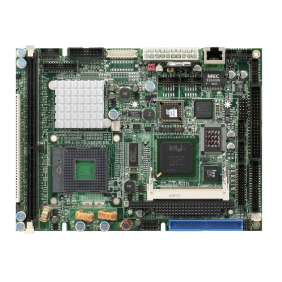
Summary of Contents for Aaeon PCM-8152
- Page 1 ® ® Intel Pentium M / Celeron M Processors One DDR 266/333 SDRAM DIMM 48-bit Dual Channel LVDS TFT LCD AC97 3D Surround 5.1Channel 4 USB 2.0 / 4 COMs / Digital IO PCM-8152 Manual Rev.A 1st Ed. Nov. 2006...
- Page 2 AAEON assumes no liabilities resulting from errors or omissions in this document, or from the use of the information contained herein. AAEON reserves the right to make changes in the product design without notice to its users.
- Page 3 C o m p a c t B o a r d P C M - 8 1 5 2 Acknowledgments All other products’ name or trademarks are properties of their respective owners. Award is a trademark of Award Software International, Inc. CompactFlash™...
- Page 4 1 9657666600 Jumper Cap • 1 1759200157 CPU Cooler Fan + Heatsink (For Socket type only) • 1 PCM-8152 CPU Card • 1 Quick Installation Guide • 1 CD-ROM for manual (in PDF format) and drivers If any of these items should be missing or damaged, please...
-
Page 5: Table Of Contents
C o m p a c t B o a r d P C M - 8 1 5 2 Contents Chapter 1 General Information 1.1 Introduction..............1-2 1.2 Features ..............1-3 1.3 Specifications ............1-4 Chapter 2 Quick Installation Guide 2.1 Safety Precautions ............ - Page 6 C o m p a c t B o a r d P C M - 8 1 5 2 2.18 DVI Connector (CN7) ..........2-15 2.19 Audio Connector (CN8)........... 2-16 2.20 LAN LED Connector (CN9) ........2-16 2.21 COM 1/2/3/4 Connector (CN10)......2-17 2.22 CPU FAN Connector (CN11) ........
- Page 7 C o m p a c t B o a r d P C M - 8 1 5 2 A.2 IT8712 Watchdog Timer Initial Program ....A-7 Appendix B I/O Information B.1 I/O Address Map ............B-2 B.2 Memory Address Map..........B-3 B.3 IRQ Mapping Chart ..........B-3 B.4 DMA Channel Assignments........B-4...
-
Page 8: Chapter 1 General Information
C o m p a c t B o a r d P C M - 8 1 5 2 Chapter General Information 1- 1 Chapter 1 General Information... -
Page 9: Introduction
This model is different from other compact boards on the market, which is deploying PC/104 interface. This major feature differs from other competitors making PCM-8152 a unique display in this niche embedded world. ®... -
Page 10: Features
C o m p a c t B o a r d P C M - 8 1 5 2 1.2 Features ® ® ® Supports Socket 478 Intel Pentium M/ Celeron M up to ® ® 1.8GHz/ Onboard Mobile Intel Celeron M Processors at 600MHz and 1GHz... -
Page 11: Specifications
C o m p a c t B o a r d P C M - 8 1 5 2 1.3 Specifications System ® Supports Socket 478 Intel ® ® Pentium M / Celeron M up to 1.8GHz (400MHz FSB) or onboard ®... - Page 12 C o m p a c t B o a r d P C M - 8 1 5 2 Power Requirement +5V/ AT/ ATX Operating Temperature F~140 F (0 C~60 Board Size 8”(L) x5.72” (W) (203mm x 146mm) Gross Weight 1.2 lb (0.5kg) Display: Support: CRT/LCD, CRT/TV, LCD/DVI, CRT/DVI, LCD/TV &...
- Page 13 C o m p a c t B o a r d P C M - 8 1 5 2 Amplifier included Two 5x2 pin headers support 4 USB 2.0 Ports Digital I/O Support 16-bit (programmable) 1- 6 Chapter 1 General Information...
-
Page 14: Chapter 2 Quick Installation Guide
C o m p a c t B o a r d P C M - 8 1 5 2 Chapter Quick Installation Guide Notice: The Quick Installation Guide is derived from Chapter 2 of user manual. For other chapters further installation instructions, please refer to the user... -
Page 15: Safety Precautions
C o m p a c t B o a r d P C M - 8 1 5 2 2.1 Safety Precautions Always completely disconnect the power cord from your board whenever you are working on it. Do not make connections while the power is on, because a sudden rush of power can damage sensitive electronic components. -
Page 16: Location Of Connectors And Jumpers
C o m p a c t B o a r d P C M - 8 1 5 2 2.2 Location of Connectors and Jumpers Component Side CN18 IDE1 PC104-1 LAN1 PC104-2 CN19 CN17 CN11 VGA1 2- 3 Chapter 2 Quick Installation Guide... - Page 17 C o m p a c t B o a r d P C M - 8 1 5 2 Solder Side 2 - 4 Chapter 2 Quick Installation Guide...
-
Page 18: Mechanical Drawing
C o m p a c t B o a r d P C M - 8 1 5 2 2.3 Mechanical Drawing Component Side 17.80 14.40 8.50 198.12 193.04 193.04 192.77 192.77 190.50 185.07 184.79 179.83 181.96 174.72 172.89 170.35 153.67 148.65... - Page 19 C o m p a c t B o a r d P C M - 8 1 5 2 Solder Side 198.12 198.12 193.04 193.04 172.89 170.35 156.08 119.38 96.69 92.88 40.64 40.64 0.00 0.00 5.08 2 - 6 Chapter 2 Quick Installation Guide...
-
Page 20: List Of Jumpers
C o m p a c t B o a r d P C M - 8 1 5 2 2.4 List of Jumpers The board has a number of jumpers that allow you to configure your system to suit your application. The table below shows the function of each of the board's jumpers: Jumpers Label... -
Page 21: List Of Connectors
C o m p a c t B o a r d P C M - 8 1 5 2 2.5 List of Connectors The board has a number of connectors that allow you to configure your system to suit your application. The table below shows the function of each board's connectors: Connectors Label... - Page 22 C o m p a c t B o a r d P C M - 8 1 5 2 IDE1 EIDE Connector VGA1 VGA Display Connector LPT1 LPT Port Connector USB1 USB 0/1Connector USB2 USB 2/3 Connector 10/100 or 100/1000 Base-TX Ethernet LAN1 Connector PCI1...
-
Page 23: Setting Jumpers
C o m p a c t B o a r d P C M - 8 1 5 2 2.6 Setting Jumpers You configure your card to match the needs of your application by setting jumpers. A jumper is the simplest kind of electric switch. It consists of two metal pins and a small metal clip (often protected by a plastic cover) that slides over the pins to connect them. -
Page 24: Atx Emulation At Power Function (Jp1)
C o m p a c t B o a r d P C M - 8 1 5 2 2.7 ATX Emulation AT Power Function (JP1) Function OFF (Default) 2.8 Audio Out Selection (JP2) Function 1-3, 2-4 W/O Amplifier 3-5, 4-6 W/ Amplifier (Default) 2.9 LCD Voltage Selection (JP3) -
Page 25: Com3 Ring/+5V/+12V Selection (Jp5)
C o m p a c t B o a r d P C M - 8 1 5 2 Ring (Default) 2.11 COM3 Ring/+5V/+12V Selection (JP5) Function +12V Ring (Default) 2.12 Clear CMOS (JP6) Function Protected (Default) Clear 2.13 TV_Out Connector (CN1) Signal Signal CVBS... -
Page 26: Audio Spdif Connector (Cn2)
C o m p a c t B o a r d P C M - 8 1 5 2 2.14 Audio SPDIF Connector (CN2) Signal Signal Front-R Front-L SURROUND-R SURROUND-L LFEOUT CENOUT SPDIFO-N SPDIFI-N 2.15 Internal LVDS Connector (CN4) Signal Signal LVDS_BKLEN... -
Page 27: Atx Power Connector (Cn5)
C o m p a c t B o a r d P C M - 8 1 5 2 LVDS_TXU1# LVDS_TXU1 LVDS_TXU2# LVDS_TXU2 LVDS_TXU3# LVDS_TXU3 PPVCC LVDS_TXUCLK# LVDS_TXUCLK 2.16 ATX Power Connector (CN5) Signal Signal +3.3V +3.3V +3.3V -12V PS_ON POWER OK +5VSB... -
Page 28: Dvi Connector (Cn7)
C o m p a c t B o a r d P C M - 8 1 5 2 LVDS_TXLCLK# LVDS_TXLCLK PPVCC LVDS_TXL0# LVDS_TXL0 LVDS_TXL1# LVDS_TXL1 LVDS_TXL2# LVDS_TXL2 LVDS_TXL3# LVDS_TXL3 LVDS_DDCPDATA LVDS_DDCPCLK LVDS_TXU0# LVDS_TXU0 LVDS_TXU1# LVDS_TXU1 LVDS_TXU2# LVDS_TXU2 LVDS_TXU3# LVDS_TXU3 PPVCC LVDS_TXUCLK#... -
Page 29: Audio Connector (Cn8)
C o m p a c t B o a r d P C M - 8 1 5 2 DVI_TD0 DVI_TD0# N.C. N.C. MDVI_DATA MDVI_CLK 2.19 Audio Connector (CN8) Signal Signal MIC_IN MIC_+2.5V LINE_IN_GND CD_GND LINE_IN_L CD_IN_L LINE_IN_R CD_GND LINE_IN_GND CD_IN_R LINE_OUT_L... -
Page 30: Com1/2/3/4 Connector (Cn10)
C o m p a c t B o a r d P C M - 8 1 5 2 2.21 COM1/2/3/4 Connector (CN10) Signal Signal DCD1 DSR1 RXD1 RTS1 TXD1 CTS1 DTR1 DCD2(422TXD-/485DATA-) 12 DSR2 RXD2(422RXD+) RTS2 TXD2(422TXD+/485DATA+) 16 CTS2 DTR2(422RXD-) DCD3... -
Page 31: Cpu Fan Connector (Cn11)
C o m p a c t B o a r d P C M - 8 1 5 2 2.22 CPU FAN Connector (CN11) Signal Speed Sense 2.23 Digital I/O-1 Connector (CN12) Address=801H Signal Signal DIO1-1 DIO1-2 DIO1-3 DIO1-4 DIO1-5 DIO1-6 DIO1-7... - Page 32 C o m p a c t B o a r d P C M - 8 1 5 2 DIO1-8 CN12 Pin8 Bit 0 U38 Pin25 (GPIO 20) 2.24 Digital I/O-2 Connector (CN13) Address=800H Signal Signal DIO2-1 DIO2-2 DIO2-3 DIO2-4 DIO2-5 DIO2-6...
-
Page 33: System Fan Connector (Cn16)
C o m p a c t B o a r d P C M - 8 1 5 2 2.25 System FAN Connector (CN16) Signal Speed Sense 2.26 IrDA Connector (CN17) Signal Signal N.C. IRRX IRTX 2.27 Internal Keyboard and Mouse Connector (CN18) Signal Signal KB_DATA... -
Page 34: Floppy Connector (Fdd1)
C o m p a c t B o a r d P C M - 8 1 5 2 IDE LED(-) IDE LED(+) External Buzzer(-) External Buzzer(+) Power LED(-) Power LED(+) Reset Switch(-) Reset Switch(+) 2.29 Floppy Connector (FDD1) Signal Signal #REDWC... -
Page 35: Eide Connector (Ide1)
C o m p a c t B o a r d P C M - 8 1 5 2 #DISK CHANGE 2.30 EIDE Connector (IDE1) Signal Signal IDE RESET DATA7 DATA8 DATA6 DATA9 DATA5 DATA10 DATA4 DATA11 DATA3 DATA12 DATA2 DATA13 DATA1... -
Page 36: Vga Display Connector (Vga1)
C o m p a c t B o a r d P C M - 8 1 5 2 2.31 VGA Display Connector (VGA1) Signal Signal VGAVCC GREEN BLUE N.C. N.C. SDATA SCLK N.C. 2.32 LPT Port Connector (LPT1) Signal Signal #STROBE... -
Page 37: Usb Connector (Usb1)
C o m p a c t B o a r d P C M - 8 1 5 2 DATA7 #ACK BUSY SELECT N.C. 2.33 USB Connector (USB1) Signal Signal USBD0# USBD0 USBD1 USBD1# 2.34 USB Connector (USB2) Signal Signal USBD2# USBD2... -
Page 38: Chapter 3 Award Bios Setup
C o m p a c t B o a r d P C M - 8 1 5 2 Chapter Award BIOS Setup Chapter 3 Award BIOS Setup 3-1... - Page 39 3. The CMOS memory has lost power and the configuration information has been erased. The PCM-8152 CMOS memory has an integral lithium battery backup for data retention. However, you will need to replace the complete unit when it finally runs down.
- Page 40 C o m p a c t B o a r d P C M - 8 1 5 2 3.2 Award BIOS Setup Awards BIOS ROM has a built-in Setup program that allows users to modify the basic system configuration. This type of information is stored in battery-backed CMOS RAM so that it retains the Setup information when the power is turned off.
- Page 41 Save CMOS value changes to CMOS and exit setup. Exit Without Saving Abandon all CMOS value changes and exit setup. You can refer to the "AAEON BIOS Item Description.pdf" file in the CD for the meaning of each setting in this chapter.
-
Page 42: Chapter 4 Driver Installation
C o m p a c t B o a r d P C M - 8 1 5 2 Chapter Driver Installation Chapter 4 Driver Installation... - Page 43 C o m p a c t B o a r d P C M - 8 1 5 2 The PCM-8152 comes with an AutoRun CD-ROM that contains all drivers and utilities that can help you to install the driver automatically.
- Page 44 C o m p a c t B o a r d P C M - 8 1 5 2 4.1 Installation: Insert the PCM-8152 CD-ROM into the CD-ROM drive and install the drivers from Step 1 to Step 4 in order. Step 1 – Install INF Driver 1.
- Page 45 C o m p a c t B o a r d P C M - 8 1 5 2 8. Click on Next 9. Select Search for a suitable driver…, then click on Next 10. Select Specify a location, then click on Next 11.
-
Page 46: Appendix A Programming The Watchdog Timer
C o m p a c t B o a r d P C M - 8 1 5 2 Appendix Programming the Watchdog Timer Appendix A Programming the Watchdog Timer... -
Page 47: Programming
C o m p a c t B o a r d P C M - 8 1 5 2 A.1 Programming PCM-8152 utilizes ITE 8712 chipset as its watchdog timer controller. Below are the procedures to complete its configuration and... - Page 48 C o m p a c t B o a r d P C M - 8 1 5 2 There are three steps to complete the configuration setup: (1) Enter the MB PnP Mode; (2) Modify the data of configuration registers;...
- Page 49 C o m p a c t B o a r d P C M - 8 1 5 2 of the key-check logic, it is necessary to perform four write opera-tions to the Special Address port (2EH). Two different enter keys are provided to select configuration ports (2Eh/2Fh) of the next step.
- Page 50 C o m p a c t B o a r d P C M - 8 1 5 2 WatchDog Timer Configuration Registers Configure Control (Index=02h) This register is write only. Its values are not sticky; that is to say, a hardware reset will automatically clear the bits, and does not require...
- Page 51 C o m p a c t B o a r d P C M - 8 1 5 2 WatchDog Timer Control Register (Index=71h, Default=00h) WatchDog Timer Configuration Register (Index=72h, Default=00h) WatchDog Timer Time-out Value Register (Index=73h, Default=00h) Appendix A Programming the Watchdog Timer...
-
Page 52: It8712 Watchdog Timer Initial Program
C o m p a c t B o a r d P C M - 8 1 5 2 A.2 IT8712 Watchdog Timer Initial Program .MODEL SMALL .CODE Main: CALL Enter_Configuration_mode CALL Check_Chip mov cl, 7 call Set_Logic_Device ;time setting mov cl, 10 ;... - Page 53 C o m p a c t B o a r d P C M - 8 1 5 2 ; game port enable mov cl, 9 call Set_Logic_Device Initial_OK: CALL Exit_Configuration_mode MOV AH,4Ch INT 21h Enter_Configuration_Mode PROC NEAR MOV SI,WORD PTR CS:[Offset Cfg_Port] MOV DX,02Eh MOV CX,04h Init_1:...
- Page 54 C o m p a c t B o a r d P C M - 8 1 5 2 Exit_Configuration_Mode ENDP Check_Chip PROC NEAR MOV AL,20h CALL Read_Configuration_Data CMP AL,87h JNE Not_Initial MOV AL,21h CALL Read_Configuration_Data CMP AL,12h JNE Not_Initial Need_Initial: Not_Initial: Check_Chip ENDP...
- Page 55 C o m p a c t B o a r d P C M - 8 1 5 2 MOV DX,WORD PTR CS:[Cfg_Port+06h] IN AL,DX Read_Configuration_Data ENDP Write_Configuration_Data PROC NEAR MOV DX,WORD PTR CS:[Cfg_Port+04h] OUT DX,AL XCHG AL,AH MOV DX,WORD PTR CS:[Cfg_Port+06h] OUT DX,AL Write_Configuration_Data ENDP Superio_Set_Reg proc near...
- Page 56 C o m p a c t B o a r d P C M - 8 1 5 2 push ax push cx xchg al,cl mov cl,07h call Superio_Set_Reg pop cx pop ax Set_Logic_Device endp ;Select 02Eh->Index Port, 02Fh->Data Port Cfg_Port DB 087h,001h,055h,055h DW 02Eh,02Fh END Main...
-
Page 57: Appendix B I/O Information
C o m p a c t B o a r d P C M - 8 1 5 2 Appendix I/O Information Appendix B I/O Information... -
Page 58: I/O Address Map
C o m p a c t B o a r d P C M - 8 1 5 2 B.1 I/O Address Map Appendix B I/O Information... -
Page 59: Memory Address Map
C o m p a c t B o a r d P C M - 8 1 5 2 B.2 Memory Address Map B.3 IRQ Mapping Chart Appendix B I/O Information... -
Page 60: Dma Channel Assignments
C o m p a c t B o a r d P C M - 8 1 5 2 B.4 DMA Channel Assignments Appendix B I/O Information...
Need help?
Do you have a question about the PCM-8152 and is the answer not in the manual?
Questions and answers