
Related Manuals for Aaeon AQ7-BT


Summary of Contents for Aaeon AQ7-BT
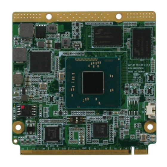
- Page 1 A Q 7 - B T AQ7-BT ® ™ Intel Atom /Celeron® Processor SoC Onboard 2GB Memory SATA x 2 USB 2.0 x 6 USB 3.0 x 1 LVDS, LCD, DP, HD Audio AQ7-BT Rev.A Manual 1 May 14, 2015 www.texim-europe.com...
- Page 2 AAEON assumes no liabilities resulting from errors or omissions in this document, or from the use of the information contained herein. AAEON reserves the right to make changes in the product design without notice to its users. www.texim-europe.com...
- Page 3 Q s e ve n M o d u l e A Q 7 - B T Acknowledgments All other products’ name or trademarks are properties of their respective owners. AMI is a trademark of American Megatrends Inc. Freescale™...
- Page 4 A Q 7 - B T Packing List Before you begin installing your card, please make sure that the following materials have been shipped: • 1 AQ7-BT CPU Module • 1 DVD-ROM for drivers and manual (in PDF format) • 2 M2.5 Screws If any of these items should be missing or damaged, please contact your distributor or sales representative immediately.
- Page 5 Q s e ve n M o d u l e A Q 7 - B T China RoHS Requirements 产品中有毒有害物质或元素名称及含量 AAEON Main Board/ Daughter Board/ Backplane 有毒有害物质或元素 部件名称 铅 汞 镉 六价铬 多溴联苯 多溴二苯醚 (Pb) (Hg) (Cd) (Cr(VI)) (PBB) (PBDE) 印刷电路板...
-
Page 6: Table Of Contents
Q s e ve n M o d u l e A Q 7 - B T Contents Chapter 1 General Information 1.1 Introduction ..............1-2 1.2 Features ..............1-3 1.3 Specifications ............1-4 Chapter 2 Quick Installation Guide 2.1 Safety Precautions ............ 2-2 2.2 Mechanical Drawings .......... - Page 7 Q s e ve n M o d u l e A Q 7 - B T B.1 I/O Address Map ............ B-2 B.2 Memory Address Map ..........B-4 B.3 IRQ Mapping Chart ..........B-6 Appendix C Programming Digital I/O C.1 Digital I/O Programming ........
-
Page 8: Chapter 1 General Information
Q s e ve n M o d u l e A Q 7 - B T Chapter General Information 1 - 1 Chapter 1 General Information www.texim-europe.com... -
Page 9: Introduction
Q s e ve n M o d u l e A Q 7 - B T 1.1 Introduction Measuring 70mm x 70mm, the AQ7-BT is a Qseven module with ® Qseven Rev.2.0 specification and equips Intel Atom™ E3800 Series Processor SoC (and the N2807 Processor) with 2GB of onboard DDR3L memory. -
Page 10: Features
Q s e ve n M o d u l e A Q 7 - B T 1.2 Features ® Intel Atom™ E3800 Series Processor SoC, N2807 Processor Onboard DDR3L 2GB Memory Gigabit Ethernet x 1 18/24-bit Single-Channel LVDS, DP/HDMI ... -
Page 11: Specifications
Q s e ve n M o d u l e A Q 7 - B T 1.3 Specifications System Form Factor ® Intel Atom™ Processor SoC Processor E3845: 4C/ 1.91GHz/ 10W E3825: 2C/1.33GHz/6W N2807: 2C/1.58GHz Onboard DDR3L 2GB System Memory Intel®... - Page 12 Q s e ve n M o d u l e A Q 7 - B T UART x 1 DC 5V Power Requirement Power Consumption (Typical) E3845: 2.7A@5V (Whole system under 100% loading) Board Size 70mm x 70mm (2.75" x 2.75") 0.2kg (0.44 lbs) Gross Weight 0 °C ~ 60 °C (32 °F ~ 140 °F) or...
- Page 13 Q s e ve n M o d u l e A Q 7 - B T (optional by request) USB 3.0 x 1 USB 2.0 x 6 4-wire UART x 1 Serial Port Audio High Definition Audio 1 - 6 Chapter 1 General Information www.texim-europe.com...
-
Page 14: Chapter 2 Quick Installation Guide
Q s e ve n M o d u l e A Q 7 - B T Chapter Quick Installation Guide Chapter 2 Quick Installation Guide www.texim-europe.com... -
Page 15: Safety Precautions
Q s e ve n M o d u l e A Q 7 - B T 2.1 Safety Precautions Always completely disconnect the power cord from your board whenever you are working on it. Do not make connections while the power is on, because a sudden rush of power can damage sensitive electronic components. -
Page 16: Mechanical Drawings
Q s e ve n M o d u l e A Q 7 - B T 2.2 Mechanical Drawings Board Component Side Solder Side Component Side Solder Side Chapter 2 Quick Installation Guide www.texim-europe.com... - Page 17 Q s e ve n M o d u l e A Q 7 - B T Heat Spreader Heat Sink Chapter 2 Quick Installation Guide www.texim-europe.com...
- Page 18 Q s e ve n M o d u l e A Q 7 - B T Cooler Chapter 2 Quick Installation Guide www.texim-europe.com...
-
Page 19: List Of Jumpers
Q s e ve n M o d u l e A Q 7 - B T 2.3 List of Jumpers The board has a jumper that allows you to configure your system to suit your application. The table below shows the function of the board's jumper: Function Label AT/ATX Setting Switch... -
Page 20: List Of Connectors
Q s e ve n M o d u l e A Q 7 - B T 2.5 List of Connectors The board has a connector that allows you to configure your system to suit your application. The table below shows the function of the board's connector: Function Label BAT1A... -
Page 21: Qseven Mxm Pin Definitions
Q s e ve n M o d u l e A Q 7 - B T 2.6 QSeven MXM Pin Definitions Chapter 2 Quick Installation Guide www.texim-europe.com... - Page 22 Q s e ve n M o d u l e A Q 7 - B T Chapter 2 Quick Installation Guide www.texim-europe.com...
-
Page 23: Qseven Mxm Pin Assignments
Q s e ve n M o d u l e A Q 7 - B T 2.7 QSeven MXM Pin Assignments Qseven SPEC AQ7-BT Signal Qseven SPEC AQ7-BT Signal Rev. 2.0 Signal Rev. 2.0 Signal 1 GND GND21 GND34... - Page 24 Q s e ve n M o d u l e A Q 7 - B T 31 SATA0_TX- SATA_TXN0 32 SATA1_TX- No connection 33 SATA_ACT# SATA_LED_CB# 34 GND GND32 35 SATA0_RX+ SATA_RXP0 36 SATA1_RX+ No connection 37 SATA0_RX- SATA_RXN0 38 SATA1_RX- No connection 39 GND...
- Page 25 Q s e ve n M o d u l e A Q 7 - B T 65 HDA_SDI/I2S_SD CB_HDA_SDI0 66 GP0_I2C_CLK EC_CLK 67 HDA_SDO/I2S_S CB_HDA_SDO 68 GP0_I2C_DAT EC_DATA 69 THRM# No connection 70 WDTRIG# No connection 71 THRMTRIP# I_THRMTRIP# 72 WDOUT O_WDT# 73 GND...
- Page 26 Q s e ve n M o d u l e A Q 7 - B T 95 USB_P1+ USB_DP1_CB 96 USB_P0+ USB_DP0_CB 97 GND GND27 98 GND GND28 99 eDP0_TX0+/LVD LVDS_A0+ 100 eDP1_TX0+/LVDS No connection S_A0+ _B0+ 101 eDP0_TX0-/LVDS LVDS_A0- 102 eDP1_TX0-/LVDS_ No connection...
- Page 27 Q s e ve n M o d u l e A Q 7 - B T 121 eDP0_AUX-/LVD LVDS_A_CLK- 122 eDP_AUX-/LVDS_ No connection S_A_CLK- B_CLK- 123 LVDS_BLT_CTR LVDS_BLT_CTR 124 GP_1-Wire_Bus No connection L/GP_PWM_OUT 125 GP2_I2C_DAT/L LVDS_DID_DAT 126 eDP0_HPD#/LVDS No connection VDS_DID_DAT _BLC_DAT 127 GP2_I2C_CLK/LV...
- Page 28 Q s e ve n M o d u l e A Q 7 - B T 145 DP_LANE2-/TMD HDMI_DP_PAIR2 146 RSVD (Diff pair) No connection S_LANE0- 147 GND GND4 148 GND GND12 149 DP_LANE0+/TM HDMI_DP_PAIR0 150 HDMI_CTRL_DAT HDMI_DATA DS_LANE2+ 151 DP_LANE0-/TMD HDMI_DP_PAIR0 152 HDMI_CTRL_CLK HDMI_CLK...
- Page 29 Q s e ve n M o d u l e A Q 7 - B T 181 PCIE0_TX- PCIE_TXN0 182 PCIE0_RX- PCIE_RXN0 183 GND GND7 184 GND GND15 185 LPC_AD0/GPIO0 LPC_GPIO_AD0 186 LPC_AD1/GPIO1 LPC_GPIO_AD1 187 LPC_AD2/GPIO2 LPC_GPIO_AD2 188 LPC_AD3/GPIO3 LPC_GPIO_AD3 189 LPC_CLK/GPIO4 CLK_LPC_GPIO_ 190 LPC_FRAME#/GPI...
- Page 30 Q s e ve n M o d u l e A Q 7 - B T 215 VCC V5_MOD_IN 216 VCC V5_MOD_IN 217 VCC V5_MOD_IN 218 VCC V5_MOD_IN 219 VCC V5_MOD_IN 220 VCC V5_MOD_IN 221 VCC V5_MOD_IN 222 VCC V5_MOD_IN 223 VCC V5_MOD_IN...
-
Page 31: Chapter 3 Ami Bios Setup
Q s e ve n M o d u l e A Q 7 - B T Chapter BIOS Setup Chapter 3 AMI BIOS Setup 3-1 www.texim-europe.com... -
Page 32: System Test And Initialization
3. The CMOS memory has lost power and the configuration information has been erased. The AQ7-BT CMOS memory has an integral lithium battery backup for data retention. However, you will need to replace the complete unit when it finally runs down. -
Page 33: Ami Bios Setup
Q s e ve n M o d u l e A Q 7 - B T 3.2 AMI BIOS Setup AMI BIOS ROM has a built-in Setup program that allows users to modify the basic system configuration. This type of information is stored in battery-backed CMOS RAM so that it retains the Setup information when the power is turned off. - Page 34 Q s e ve n M o d u l e A Q 7 - B T BIOS Setup Menu Main Press ‘Delete’ Key to enter Setup Chapter 3 AMI BIOS Setup 3-4 www.texim-europe.com...
- Page 35 Q s e ve n M o d u l e A Q 7 - B T Advanced Chapter 3 AMI BIOS Setup 3-5 www.texim-europe.com...
- Page 36 Q s e ve n M o d u l e A Q 7 - B T Advanced -> CPU Configuration Options summary: Intel Disabled Optimal Default, Failsafe Default Virtualization Enabled Technology When enabled, a VMM can utilize the additional hardware capabilities provided by Vander pool Technology Chapter 3 AMI BIOS Setup 3-6 www.texim-europe.com...
- Page 37 Q s e ve n M o d u l e A Q 7 - B T Advanced -> IDE Configuration Options summary: SATA Mode AHCI Default IDE: Configure SATA controllers as legacy IDE AHCI: Configure SATA controllers to operate in AHCI mode Serial-ATA Port0/1 Enabled Default...
- Page 38 Q s e ve n M o d u l e A Q 7 - B T Advanced -> LPSS & SCC Configuration Options summary: LPSS & SCC Devices ACPI mode Default Mode PCI mode SCC SD Card Support Enabled Default Disable DDR50 Support for...
- Page 39 Q s e ve n M o d u l e A Q 7 - B T Per chipset spec, there is chance that SD card can’t be recognized properly when set to high speed. (DDR50) The issue doesn’t occur at low speed setting.
- Page 40 Q s e ve n M o d u l e A Q 7 - B T Enables BIOS Support for Legacy USB Support. When enabled, USB can be functional in legacy environment like DOS. AUTO option disables legacy support if no USB devices are connected Device Name Auto Optimal Default, Failsafe...
- Page 41 Q s e ve n M o d u l e A Q 7 - B T Advanced -> On-Module H/W Monitor Chapter 3 AMI BIOS Setup 3-11 www.texim-europe.com...
- Page 42 Q s e ve n M o d u l e A Q 7 - B T Advanced -> Dynamic Digital IO Options summary: GPI[3:0] Input Optimal Default, Failsafe Default Direction Output Set GPI[3:0] as Input or Output GPI[3:0] Output Optimal Default, Failsafe Default Level Set GPI[3:0] Output as Hi or Low...
- Page 43 Q s e ve n M o d u l e A Q 7 - B T GPO[3:0] Output Input Level Output Optimal Default, Failsafe Default Set GPO[3:0] Output as Hi or Low Chapter 3 AMI BIOS Setup 3-13 www.texim-europe.com...
- Page 44 Q s e ve n M o d u l e A Q 7 - B T Advanced -> Power Management Options summary: Power Mode ATX Type Optimal Default, Failsafe Default AT Type Select power supply mode Restore AC Last State Optimal Default, Failsafe Default Power Loss Power On...
- Page 45 Q s e ve n M o d u l e A Q 7 - B T from S5 Dynamic Time Enable or disable System wake on alarm event. When enabled, System will wake on the hr::min::sec specified Chapter 3 AMI BIOS Setup 3-15 www.texim-europe.com...
- Page 46 Q s e ve n M o d u l e A Q 7 - B T Advanced -> SIO Configuration Chapter 3 AMI BIOS Setup 3-16 www.texim-europe.com...
- Page 47 Q s e ve n M o d u l e A Q 7 - B T Advanced -> Serial Port Configuration Options summary: Use This Device Disabled Optimal Default, Failsafe Enabled Default En/Disable Serial Port (COM) Possible: Use Automatic Settings Optimal Default, Failsafe Default IO=2D8;...
- Page 48 Q s e ve n M o d u l e A Q 7 - B T Chipset Chapter 3 AMI BIOS Setup 3-18 www.texim-europe.com...
- Page 49 Q s e ve n M o d u l e A Q 7 - B T Chipset -> North Bridge Chapter 3 AMI BIOS Setup 3-19 www.texim-europe.com...
- Page 50 Q s e ve n M o d u l e A Q 7 - B T Chipset -> North Bridge -> Display Control Configuration Options summary: DVMT Optimal Default, Failsafe Pre-Allocated Default 128M 160M ….. 512M DVMT Total Gfx 128MB 256MB Optimal Default, Failsafe...
- Page 51 Q s e ve n M o d u l e A Q 7 - B T Primary IGFX Boot VBIOS Default Optimal Default, Failsafe Display Default LVDS DP/HDMI Select the Video Device which will be activated during POST. This has no effect if external graphics present.
- Page 52 Q s e ve n M o d u l e A Q 7 - B T 1366x768 1440x900 Select Panel Type 1024x768 Color Depth 18-Bit Optimal Default, Failsafe Default 24-Bit Backlight Type Normal Optimal Default, Failsafe Default Inverted Backlight Level Optimal Default, Failsafe Default 100%...
- Page 53 Q s e ve n M o d u l e A Q 7 - B T Chipset -> South Bridge Options summary: Audio Controller Enabled Default Disable PCI Express Port Enabled Default 0/1/2/3 Disabled Hot Plug Disabled Enabled Default Speed Auto Default...
- Page 54 Q s e ve n M o d u l e A Q 7 - B T Security Setup submenu: Security Change User/Supervisor Password You can install a Supervisor password, and if you install a supervisor password, you can then install a user password. A user password does not provide access to many of the features in the Setup utility.
- Page 55 Q s e ve n M o d u l e A Q 7 - B T confirmation. Press Enter after you have retyped it correctly. The password is required at boot time, or when the user enters the Setup utility. Removing the Password Highlight this item and type in the current password.
- Page 56 Q s e ve n M o d u l e A Q 7 - B T Boot Options summary: Quiet Boot Disabled Enabled Default En/Disable showing boot logo. Option Rom Message Force BIOS Default Keep Current Launch PXE OpROM Disabled Default Enabled...
- Page 57 Q s e ve n M o d u l e A Q 7 - B T Exit Chapter 3 AMI BIOS Setup 3-27 www.texim-europe.com...
-
Page 58: Chapter 4 Driver Installation
Q s e ve n M o d u l e A Q 7 - B T Chapter Driver Installation Chapter 4 Driver Installation www.texim-europe.com... - Page 59 Q s e ve n M o d u l e A Q 7 - B T The AQ7-BT comes with a driver disk that contains all drivers and utilities you need to setup your product. Insert the disk and the installation guide will start automatically. If it doesn’t, please follow the sequence below to install the drivers.
- Page 60 Q s e ve n M o d u l e A Q 7 - B T 4.1 Installation Insert the AQ7-BT driver disk into the disk drive and install the drivers from Step 1 to Step 8 in order. Step 1 – Install Chipset Driver 1.
- Page 61 Q s e ve n M o d u l e A Q 7 - B T Step 4 – Install Audio Driver 1. Open the STEP4 - LAN folder followed by win7_8-32_64_R273.exe 2. Follow the instructions 3. Drivers will be installed automatically Step 5 –...
- Page 62 Q s e ve n M o d u l e A Q 7 - B T 2. Open the.msi file in the folder 3. Follow the instructions 4. Drivers will be installed automatically Chapter 4 Driver Installation www.texim-europe.com...
-
Page 63: Appendix A Programming The Watchdog Timer
Q S e ve n M o d u l e A Q 7 - B T Appendix Programming the Watchdog Timer Appendix A Programming the Watchdog Timer A-1 www.texim-europe.com... -
Page 64: Watchdog Timer Initial Program
Q S e ve n M o d u l e A Q 7 - B T A.1 Watchdog Timer Initial Program Table 1 : Embedded BRAM relative register table Default Value Note Index 0x284 BRAM Index Register (Note1) Data 0x285 BRAM Data Register (Note2) - Page 65 Q S e ve n M o d u l e A Q 7 - B T ************************************************************************************ // Embedded BRAM relative definition (Please reference to Table 1) #define byte EcBRAMIndex //This parameter is represented from Note1 #define byte EcBRAMData //This parameter is represented from Note2 #define byte BRAMLDNReg //This parameter is represented from Note3 #define byte BRAMFnDataReg //This parameter is represented from Note4 #define void EcBRAMWriteByte(byte Offset, byte Value);...
- Page 66 Q S e ve n M o d u l e A Q 7 - B T ************************************************************************************ Main VOID // Procedure : AaeonWDTConfig // (byte)Timer : Time of WDT timer.(0x00~0xFF) // (boolean)Unit : Select time unit(0: second, 1: minute). AaeonWDTConfig();...
- Page 67 Q S e ve n M o d u l e A Q 7 - B T ************************************************************************************ // Procedure : AaeonWDTEnable AaeonWDTEnable () VOID WDTEnableDisable( // Procedure : AaeonWDTConfig AaeonWDTConfig () VOID // Disable WDT counting WDTEnableDisable( // WDT relative parameter setting WDTParameterSetting();...
- Page 68 Q S e ve n M o d u l e A Q 7 - B T ************************************************************************************ ECBRAMWriteByte(byte OPReg, byte OPBit, byte Value) VOID IOWriteByte(EcBRAMIndex, 0x10); IOWriteByte(EcBRAMData, BRAMLDNReg); IOWriteByte(EcBRAMIndex, 0x11); IOWriteByte(EcBRAMData, BRAMFnDataReg); IOWriteByte(EcBRAMIndex, 0x13 + OPReg); IOWriteByte(EcBRAMData, Value); IOWriteByte(EcBRAMIndex, 0x12); IOWriteByte(EcBRAMData, 0x30);...
-
Page 69: Appendix B I/O Information
Q S e ve n M o d u l e A Q 7 - B T Appendix I/O Information B - 1 Appendix B I/O Information www.texim-europe.com... -
Page 70: I/O Address Map
Q S e ve n M o d u l e A Q 7 - B T B.1 I/O Address Map B - 2 Appendix B I/O Information www.texim-europe.com... - Page 71 Q S e ve n M o d u l e A Q 7 - B T B - 3 Appendix B I/O Information www.texim-europe.com...
-
Page 72: Memory Address Map
Q S e ve n M o d u l e A Q 7 - B T B.2 Memory Address Map B - 4 Appendix B I/O Information www.texim-europe.com... - Page 73 Q S e ve n M o d u l e A Q 7 - B T B - 5 Appendix B I/O Information www.texim-europe.com...
-
Page 74: Irq Mapping Chart
Q S e ve n M o d u l e A Q 7 - B T B.3 IRQ Mapping Chart B - 6 Appendix B I/O Information www.texim-europe.com... - Page 75 Q S e ve n M o d u l e A Q 7 - B T B - 7 Appendix B I/O Information www.texim-europe.com...
- Page 76 Q S e ve n M o d u l e A Q 7 - B T B - 8 Appendix B I/O Information www.texim-europe.com...
- Page 77 Q S e ve n M o d u l e A Q 7 - B T B - 9 Appendix B I/O Information www.texim-europe.com...
- Page 78 Q S e ve n M o d u l e A Q 7 - B T B - 10 Appendix B I/O Information www.texim-europe.com...
- Page 79 Q S e ve n M o d u l e A Q 7 - B T B - 11 Appendix B I/O Information www.texim-europe.com...
- Page 80 Q S e ve n M o d u l e A Q 7 - B T B - 12 Appendix B I/O Information www.texim-europe.com...
- Page 81 Q S e ve n M o d u l e A Q 7 - B T B - 13 Appendix B I/O Information www.texim-europe.com...
- Page 82 Q S e ve n M o d u l e A Q 7 - B T B - 14 Appendix B I/O Information www.texim-europe.com...
- Page 83 Q S e ve n M o d u l e A Q 7 - B T B - 15 Appendix B I/O Information www.texim-europe.com...
- Page 84 Q S e ve n M o d u l e A Q 7 - B T B - 16 Appendix B I/O Information www.texim-europe.com...
- Page 85 Q S e ve n M o d u l e A Q 7 - B T B - 17 Appendix B I/O Information www.texim-europe.com...
- Page 86 Q S e ve n M o d u l e A Q 7 - B T B - 18 Appendix B I/O Information www.texim-europe.com...
-
Page 87: Appendix C Programming Digital I/O
Q S e ve n M o d u l e A Q 7 - B T Appendix Programming Digital I/O Appendix D Electrical Specifications for I/O Ports www.texim-europe.com... -
Page 88: Digital I/O Programming
Q S e ve n M o d u l e A Q 7 - B T C.1 Digital I/O Programming The AQ7-BT utilizes the ITE8525VG chipset as its Digital I/O controller. Below are the procedures to complete its configuration which you can develop customized program to fit your application. - Page 89 Q S e ve n M o d u l e A Q 7 - B T C.2 Digital I/O Register Table 1 : Embedded BRAM relative register table Default Note Value Index 0x284 BRAM Index Register (Note1) Data 0x285 BRAM Data Register (Note2) Logical Device Number...
-
Page 90: Digital I/O Sample Program
Q S e ve n M o d u l e A Q 7 - B T C.3 Digital I/O Sample Program ************************************************************************************ // Embedded BRAM relative definition (Please reference to Table 1) #define byte EcBRAMIndex //This parameter is represented from Note1 #define byte EcBRAMData //This parameter is represented from Note2 #define byte BRAMLDNReg //This parameter is represented from Note3 #define byte BRAMFnData0Reg //This parameter is represented from Note4... - Page 91 Q S e ve n M o d u l e A Q 7 - B T ************************************************************************************ Main VOID Boolean PinStatus ; // Procedure : AaeonReadPinStatus // Input : Example, Read Digital I/O Pin 3 status // Output : InputStatus : 0: Digital I/O Pin level is low 1: Digital I/O Pin level is High...
- Page 92 Q S e ve n M o d u l e A Q 7 - B T ************************************************************************************ AaeonReadPinStatus(byte OptionReg, byte BitNum) Boolean Byte TempByte; TempByte = ECBRAMReadByte(BRAMFnData1Reg, OptionReg); If (TempByte & BitNum == 0) Return 0; Return 1; AaeonSetOutputLevel(byte OptionReg, byte BitNum, byte VOID Value) Byte TempByte;...
- Page 93 Q S e ve n M o d u l e A Q 7 - B T ************************************************************************************ ECBRAMWriteByte(byte OPReg, byte OPBit, byte Value) VOID IOWriteByte(EcBRAMIndex, 0x10); IOWriteByte(EcBRAMData, BRAMLDNReg); IOWriteByte(EcBRAMIndex, 0x11); IOWriteByte(EcBRAMData, BRAMFnDataReg); IOWriteByte(EcBRAMIndex, 0x13 + OPReg); IOWriteByte(EcBRAMData, Value); IOWriteByte(EcBRAMIndex, 0x12); IOWriteByte(EcBRAMData, 0x30);...
Need help?
Do you have a question about the AQ7-BT and is the answer not in the manual?
Questions and answers