Table of Contents
Advertisement
Quick Links
Download this manual
See also:
Manual
Advertisement
Table of Contents

Related Manuals for Aaeon PFM-540I


Summary of Contents for Aaeon PFM-540I
- Page 1 P F M - 5 4 0 I PFM-540I ® Geode LX 800 Processor AMD LX 800 +CS 5536 RTL8139DL for 10/100Mbps 18/24-bit TFT LCD Panel 2 COM, 4 USB, 1 IrDA PFM-540I Manual Rev.A 2nd Ed. June 25, 2014...
- Page 2 AAEON assumes no liabilities resulting from errors or omissions in this document, or from the use of the information contained herein. AAEON reserves the right to make changes in the product design without notice to its users.
- Page 3 P C 1 0 4 C P U M o d u l e P F M - 5 4 0 I Acknowledgments All other products’ name or trademarks are properties of their respective owners. Award is a trademark of Award Software International, Inc. ...
- Page 4 P F M - 5 4 0 I Packing List Before you begin installing your card, please make sure that the following materials have been shipped: 9681540I00 Cable Kit for PFM-540I 1701160201 VGA cable x 1 1701260201 Printer Port Cable x 1 1709100201...
-
Page 5: Table Of Contents
P C 1 0 4 C P U M o d u l e P F M - 5 4 0 I Contents Chapter 1 General Information 1.1 Introduction ..............1-2 1.2 Features ..............1-3 1.3 Specifications ............1-4 Chapter 2 Quick Installation Guide 2.1 Safety Precautions ............ - Page 6 P C 1 0 4 C P U M o d u l e P F M - 5 4 0 I 2.17 IDE Connector (CN9) ..........2-12 2.18 COM1 Connector (CN10) ........2-13 2.19 Floppy Connector (CN11) ........2-13 2.20 Power Connector (CN12) ........
- Page 7 P C 1 0 4 C P U M o d u l e P F M - 5 4 0 I Appendix B I/O Information B.1 I/O Address Map ............ B-2 B.2 Memory Address Map ..........B-3 B.3 IRQ Mapping Chart ..........B-4 B.4 DMA Channel Assignments ........
-
Page 8: Chapter 1 General Information
P C 1 0 4 C P U M o d u l e P F M - 5 4 0 I Chapter General Information 1- 1 Chapter 1 General Information... -
Page 9: Introduction
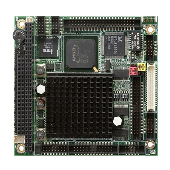
10/100Base-TX Ethernet port, four USB 2.0 ports, two serial ports, one parallel port, IR interface, watchdog timer and includes PC/104 expansion. PFM-540I is a RoHS compliant product that is fanless and fully supports ISA and CFD. For Operating Systems, it supports regular embedded OS, such as WinCE, and WinXP Embedded, Windows XP Professional for easy compatibility with customers’... - Page 10 P C 1 0 4 C P U M o d u l e P F M - 5 4 0 I 1.2 Features AMD Geode LX800 (500MHz) Processor Supports Onboard DDR SDRAM, Max. 1GB for DDR333 and 512MB for DDR400 Supports 18/24-bit TFT LCD panel Supports CFD Type I, ATA-33 Supports 4 USB 2.0 ports, 2 COM ports and 1 Parallel port...
-
Page 11: Specifications
P C 1 0 4 C P U M o d u l e P F M - 5 4 0 I 1.3 Specifications System Processor AMD Geode LX 800 (500MHz) Processor System Memory 200-pin Onboard DDR SDRAM SODIMM x 1, Max. 1GB for DDR333 and 512MB for DDR 400 (Please refer to the Quick Installation Guide 2.26 DDR1 SODIMM Slot for details) - Page 12 P C 1 0 4 C P U M o d u l e P F M - 5 4 0 I Display Chipset AMD LX 800 Memory Shared system memory up to 254 MB Resolution Up to 1920 x 1440 @ 32bpp for CRT Up to 1024 x 768 @ 24bpp for LCD LCD Interface Up to 18/24-bit TTL TFT LCD...
-
Page 13: Chapter 2 Quick Installation Guide
P C 1 0 4 C P U M o d u l e P F M - 5 4 0 I Chapter Quick Installation Guide 2 - 1 Chapter 2 Quick Installation Guide... -
Page 14: Safety Precautions
P C 1 0 4 C P U M o d u l e P F M - 5 4 0 I 2.1 Safety Precautions Always completely disconnect the power cord from your board whenever you are working on it. Do not make connections while the power is on, because a sudden rush of power can damage sensitive electronic components. -
Page 15: Location And Mechanical Drawing Of Connectors And
P C 1 0 4 C P U M o d u l e P F M - 5 4 0 I 2.2 Location and Mechanical Drawing of Connectors and Jumpers Component Side Component Side 2- 3 Chapter 2 Quick Installation Guide... - Page 16 P C 1 0 4 C P U M o d u l e P F M - 5 4 0 I Solder Side Solder Side 2 - 4 Chapter 2 Quick Installation Guide...
-
Page 17: List Of Jumpers
P C 1 0 4 C P U M o d u l e P F M - 5 4 0 I 2.3 List of Jumpers The board has a number of jumpers that allow you to configure your system to suit your application. The table below shows the function of each of the board's jumpers: Jumpers Label... - Page 18 P C 1 0 4 C P U M o d u l e P F M - 5 4 0 I USB Connector PC104 Connector LPT Port Connector IDE Connector COM1 Connector CN10 CN11 Floppy Connector CN12 Power Connector CN13 COM2 Connector CN14...
-
Page 19: Setting Jumpers
P C 1 0 4 C P U M o d u l e P F M - 5 4 0 I 2.5 Setting Jumpers You configure your card to match the needs of your application by setting jumpers. A jumper is the simplest kind of electric switch. It consists of two metal pins and a small metal clip (often protected by a plastic cover) that slides over the pins to connect them. -
Page 20: Cfd Master/Slave Selection (Jp1)
P C 1 0 4 C P U M o d u l e P F M - 5 4 0 I 2.6 CFD Master/Slave Selection (JP1) Function Slave Master (Default) 2.7 RS-232 Ring/5V Selection (JP2) Function COM1 Ring (Default) COM2 Ring (Default) 2.8 LCD Clock Selection and Clear CMOS (JP3) -
Page 21: Front Panel Connector (Cn1)
P C 1 0 4 C P U M o d u l e P F M - 5 4 0 I 2.9 Front Panel Connector (CN1) Signal Signal Power LED (+) Power LED (-) N.C. Speaker (+) Speaker(-) N.C. IDE LED(+) IDE LED(-) N.C. -
Page 22: Usb 3-4 Connector (Cn4)
P C 1 0 4 C P U M o d u l e P F M - 5 4 0 I 2.12 USB 3-4 Connector (CN4) Signal Signal USBD3- USBD3+ USBD4+ USBD4- 2.13 VGA Display Connector (CN5) Signal Signal GREEN BLUE N.C. -
Page 23: Pc 104 Connector (Cn7)
P F M - 5 4 0 I USBD1- USBD1+ USBD2+ USBD2- 2.15 PC 104 Connector (CN7) As standard. Note: PFM-540I does not support ISA card with DMA or Master mode in PC/104 interface. 2.16 LPT Port Connector (CN8) Signal Signal #STROBE #AFD... -
Page 24: Ide Connector (Cn9)
P C 1 0 4 C P U M o d u l e P F M - 5 4 0 I SELECT N.C. 2.17 IDE Connector (CN9) Signal Signal #RESET DATA7 DATA8 DATA6 DATA9 DATA5 DATA10 DATA4 DATA11 DATA3 DATA12 DATA2 DATA13... -
Page 25: Com1 Connector (Cn10)
P C 1 0 4 C P U M o d u l e P F M - 5 4 0 I N.C. Note: The IDE interface on PFM-540I only supports two IDE devices. If you use a CF card, there is only one IDE device usable. 2.18 COM1 Connector (CN10) -
Page 26: Power Connector (Cn12)
P C 1 0 4 C P U M o d u l e P F M - 5 4 0 I #STEP #WRITE DATA #WRITE GATE #TRACK0 #WRITE PROTECT N.C. #READ DATA #HDSEL N.C. #DISK CHANGE 2.20 Power Connector (CN12) Signal Signal +12V... -
Page 27: Ethernet Connector (Cn14)
P C 1 0 4 C P U M o d u l e P F M - 5 4 0 I 2.22 Ethernet Connector (CN14) Signal Signal N.C. N.C. CHASSIS_GND CHASSIS_GND N.C. N.C. 2.23 LCD Connector (CN15) 24-bit TTL Signal Signal +3.3V... - Page 28 P C 1 0 4 C P U M o d u l e P F M - 5 4 0 I RED0 RED1 RED2 RED3 RED4 RED5 RED6 RED7 CLOCK VSYNC HSYNC N.C. ENAVEE 18-bit TTL Signal Signal +3.3V +3.3V ENBKL BLUE0...
-
Page 29: Battery Connector (Bat1)
P C 1 0 4 C P U M o d u l e P F M - 5 4 0 I RED0 RED1 RED2 RED3 RED4 RED5 CLOCK VSYNC HSYNC ENAVEE 2.24 Battery Connector (BAT1) Signal Signal 2.25 DDR1 SODIMM Slot (SODIMM1 ) Standard SODIMM Slot Note from AMD: Memory configurations supported. - Page 30 P C 1 0 4 C P U M o d u l e P F M - 5 4 0 I 333MHz F2F100FFh/ 56960004h 1: Maximum memory is assuming 1Gbit devices. 2 - 18 Chapter 2 Quick Installation Guide...
- Page 31 P C 1 0 4 C P U M o d u l e P F M - 5 4 0 I Below Table for China RoHS Requirements 产品中有毒有害物质或元素名称及含量 AAEON Main Board/ Daughter Board/ Backplane 有毒有害物质或元素 部件名称 铅 汞 镉...
-
Page 32: Chapter 3 Award Bios Setup
P C 1 0 4 C P U M o d u l e P F M - 5 4 0 I Chapter Award BIOS Setup Chapter 3 Award BIOS Setup 3-1... - Page 33 3. The CMOS memory has lost power and the configuration information has been erased. The PFM-540I CMOS memory has an integral lithium battery backup for data retention. However, you will need to replace the complete unit when it finally runs down.
- Page 34 P C 1 0 4 C P U M o d u l e P F M - 5 4 0 I 3.2 Award BIOS Setup Awards BIOS ROM has a built-in Setup program that allows users to modify the basic system configuration. This type of information is stored in battery-backed CMOS RAM so that it retains the Setup information when the power is turned off.
- Page 35 P C 1 0 4 C P U M o d u l e P F M - 5 4 0 I Advanced Chipset Features Use this menu to change the values in the chipset registers and optimize your system performance. Integrated Peripherals Use this menu to specify your settings for integrated peripherals.
- Page 36 Save CMOS value changes to CMOS and exit setup. Exit Without Saving Abandon all CMOS value changes and exit setup. You can refer to the “ AAEON BIOS Item Description.pdf” file in the CD for the meaning of each setting in this chapter.
-
Page 37: Chapter 4 Driver Installation
P C 1 0 4 C P U M o d u l e P F M - 5 4 0 I Chapter Driv Installation 4 - 1 Chapter 4 Driver Installation... -
Page 38: Software Drivers
P C 1 0 4 C P U M o d u l e P F M - 5 4 0 I 4.1 Software Drivers This chapter describes the operation and installation of the display drivers supplied on the Supporting CD-ROM that are shipped with your product. -
Page 39: Necessary To Know
P C 1 0 4 C P U M o d u l e P F M - 5 4 0 I 4.2 Necessary to Know The instructions in this manual assume that you understand elementary concepts of MS-DOS and the IBM Personal Computer. Before you attempt to install any driver from the Supporting CD-ROM, you should: Know how to copy files from a CD-ROM to a directory on the... -
Page 40: Installing Vga Driver
P C 1 0 4 C P U M o d u l e P F M - 5 4 0 I 4.3 Installing VGA Driver Win XP / Win XPe VGA Place the Driver CD-ROM into your CD-ROM drive and follow the steps below to install. -
Page 41: Installing Aes Driver
P C 1 0 4 C P U M o d u l e P F M - 5 4 0 I 4.4 Installing AES Driver Win XP / Win XPe Geode LX AES Crypto Place the Driver CD-ROM into your CD-ROM drive and follow the steps below to install. -
Page 42: Installing Pci To Isa Bridge Driver
P C 1 0 4 C P U M o d u l e P F M - 5 4 0 I 4.5 Installing PCI to ISA Bridge Driver Win XP / Win XPe System Place the Driver CD-ROM into your CD-ROM drive and follow the steps below to install. -
Page 43: Installing Ethernet Driver
P C 1 0 4 C P U M o d u l e P F M - 5 4 0 I 4.6 Installing Ethernet Driver 1. Click on the Step 4 –Install Lan folder. 2. Double click on the Setup file located in the folder. 3. - Page 44 P C 1 0 4 C P U M o d u l e P F M - 5 4 0 I guide displayed at the bottom of the screen for additional information. After you have made your selections and the configuration is what you want, press <ESC>.
-
Page 45: Appendix A Programming The Watchdog Timer
P C 1 0 4 C P U M o d u l e P F M - 5 4 0 I Appendix Programming the Watchdog Timer Appendix A Programming the Watchdog Timer A-1... -
Page 46: Programming
PFM-540I utilizes IT8712F-A chipset as its watchdog timer controller. Below are the procedures to complete its configuration and the AAEON intial watchdog timer program is also attached based on which you can develop customized program to fit your application. Configuring Sequence Description After the hardware reset or power-on reset, the IT8712F-A enters the normal mode with all logical devices disabled except KBC. - Page 47 P C 1 0 4 C P U M o d u l e P F M - 5 4 0 I There are three steps to complete the configuration setup: (1) Enter the MB PnP Mode; (2) Modify the data of configuration registers; (3) Exit the MB PnP Mode.
- Page 48 P C 1 0 4 C P U M o d u l e P F M - 5 4 0 I WatchDog Timer Configuration Registers Configure Control (Index=02h) This register is write only. Its values are not sticky; that is to say, a hardware reset will automatically clear the bits, and does not require the software to clear them.
- Page 49 P C 1 0 4 C P U M o d u l e P F M - 5 4 0 I WatchDog Timer Configuration Register (Index=72h, Default=00h) WatchDog Timer Time-out Value Register (Index=73h, Default=00h) Appendix A Programming the Watchdog Timer A-5...
-
Page 50: It8712F-A Watchdog Timer Initial Program
P C 1 0 4 C P U M o d u l e P F M - 5 4 0 I A.2 IT8712F-A Watchdog Timer Initial Program .MODEL SMALL .CODE Main: CALL Enter_Configuration_mode CALL Check_Chip mov cl, 7 call Set_Logic_Device ;time setting mov cl, 10 ;... - Page 51 P C 1 0 4 C P U M o d u l e P F M - 5 4 0 I ; game port enable mov cl, 9 call Set_Logic_Device Initial_OK: CALL Exit_Configuration_mode MOV AH,4Ch INT 21h Enter_Configuration_Mode PROC NEAR MOV SI,WORD PTR CS:[Offset Cfg_Port] MOV DX,02Eh MOV CX,04h...
- Page 52 P C 1 0 4 C P U M o d u l e P F M - 5 4 0 I Exit_Configuration_Mode ENDP Check_Chip PROC NEAR MOV AL,20h CALL Read_Configuration_Data CMP AL,87h JNE Not_Initial MOV AL,21h CALL Read_Configuration_Data CMP AL,12h JNE Not_Initial Need_Initial: Not_Initial:...
- Page 53 P C 1 0 4 C P U M o d u l e P F M - 5 4 0 I MOV DX,WORD PTR CS:[Cfg_Port+06h] IN AL,DX Read_Configuration_Data ENDP Write_Configuration_Data PROC NEAR MOV DX,WORD PTR CS:[Cfg_Port+04h] OUT DX,AL XCHG AL,AH MOV DX,WORD PTR CS:[Cfg_Port+06h] OUT DX,AL Write_Configuration_Data ENDP...
- Page 54 P C 1 0 4 C P U M o d u l e P F M - 5 4 0 I push ax push cx xchg al,cl mov cl,07h call Superio_Set_Reg pop cx pop ax Set_Logic_Device endp ;Select 02Eh->Index Port, 02Fh->Data Port Cfg_Port DB 087h,001h,055h,055h DW 02Eh,02Fh END Main...
-
Page 55: Appendix B I/O Information
P C 1 0 4 C P U M o d u l e P F M - 5 4 0 I Appendix I/O Information B - 1 Appendix B I/O Information... -
Page 56: I/O Address Map
P C 1 0 4 C P U M o d u l e P F M - 5 4 0 I B.1 I/O Address Map B - 2 Appendix B I/O Information... -
Page 57: Memory Address Map
P C 1 0 4 C P U M o d u l e P F M - 5 4 0 I B.2 1 MB Memory Address Map B - 3 Appendix B I/O Informaion... -
Page 58: Irq Mapping Chart
P C 1 0 4 C P U M o d u l e P F M - 5 4 0 I B.3 IRQ Mapping Chart B.4 DMA Channel Assignments B - 4 Appendix B I/O Information... -
Page 59: Appendix C Mating Connector
P C 1 0 4 C P U M o d u l e P F M - 5 4 0 I Appendi Mating Connecotor C - 1 Appendix C Mating Connector... -
Page 60: List Of Mating Connectors And Cables
P C 1 0 4 C P U M o d u l e P F M - 5 4 0 I C.1 List of Mating Connectors and Cables The table notes mating connectors and available cables. Connector Function Mating Connector Available Cable AAEON Cable Label Vendor Model no Front Neltron 2226A-XX Panel... - Page 61 P C 1 0 4 C P U M o d u l e P F M - 5 4 0 I Keentop 1014 1701440350 IDE Cable Connector Series COM1 Keentop 1014 1701100207 CN10 Serial Port Cable Connector Series Floppy Keentop 1014 1701340703 CN11...
Need help?
Do you have a question about the PFM-540I and is the answer not in the manual?
Questions and answers