
Subscribe to Our Youtube Channel
Related Manuals for Contec DAI12-4GY


Summary of Contents for Contec DAI12-4GY
- Page 1 F&eIT Series Isolated Analog Output Module DAI12-4(FIT)GY User’s Manual CONTEC CO., LTD.
- Page 2 Check Your Package Thank you for purchasing the CONTEC product. The product consists of the items listed below. Check, with the following list, that your package is complete. If you discover damaged or missing items, contact your retailer. Product Configuration List - Module …1...
-
Page 3: Trademarks
No part of this document may be copied or reproduced in any form by any means without prior written consent of CONTEC CO., LTD. CONTEC CO., LTD. makes no commitment to update or keep current the information contained in this document. -
Page 4: Table Of Contents
Table of Contents Check Your Package ............i Copyright................ii Trademarks ............... ii Table of Contents ............. iii 1. Introduction ..............1 Features ................ 1 Functions and control method by controller connected2 Limited One-Year Warranty ........4 How to Obtain Service..........4 Liability ................. - Page 5 Software Mode ............32 Clock Mode (No Interrupts) ........34 Clock Mode (with Interrupts) ........37 5. Using the Memory Address Map ........43 Module Settings Area ..........44 Module Information Area ........... 47 Basic Output Data Area ..........49 Examples.................
-
Page 6: Introduction
Introduction Introduction Congratulations on your recent purchase of an Insulator Digital Output Module. The DAI12-4(FIT)GY can control external devices by converting digital data that is output from a, F&eIT-series controller module <CPU-CAxx(FIT)GY, CPU-SBxx(FIT)GY etc> into either voltage or current-based analog signals. The insulation between external signals and the Controller Module permits the use of the Controller Module without compromising the communications features of the latter. -
Page 7: Functions And Control Method By Controller Connected2
Introduction Functions and control method by controller connected The DAI12-4(FIT)GY can be connected to a variety of controllers. Micro Controller Unit : CPU-SBxx(FIT)GY I/O Controller Module : CPU-CAxx(FIT)GY Monitoring & Control Server Unit : SVR-MMF2(FIT) Monitoring & Control Server Unit : SVR-MMF(FIT)GY Isolated Analog Output Module for USB : DAI12-4 (USB)GY... - Page 8 Introduction Control method by controller connected Control using the I/O address map ο Control using the memory address map ο FIT Protocol ο API-CAP(W32) ο Control via the Windows driver * API-SBP(W32) ο ο ο API-USBP(WDM) Control over the web ο...
-
Page 9: Limited One-Year Warranty
Introduction Limited One-Year Warranty CONTEC F&eIT products are warranted by CONTEC CO., LTD. to be free from defects in material and workmanship for up to one year from the date of purchase by the original purchaser. Repair will be free of charge only when this product is returned freight prepaid with a copy of the original invoice and a Return Merchandise Authorization to the distributor or the CONTEC group office, from which it was purchased. -
Page 10: Handling Precautions
Handling Precautions Take the following precautions when handling this module. - Do not modify the module. CONTEC will bear no responsibility for any problems, etc., resulting from modifying this module. - Do not use or store the equipment in a hot or cold place, or in a place that is subject to severe temperature changes (Operating temperature range: 0 - 50°C). -
Page 11: About The Manual
Introduction FCC PART 15 Class A Notice NOTE This equipment has been tested and found to comply with the limits for a Class A digital device, pursuant to part 15 of the FCC Rules. These limits are designed to provide reasonable protection against harmful interference when the equipment is operated in commercial environment. -
Page 12: Module Nomenclature And Settings
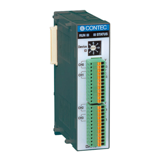
Module Nomenclature and Settings Module Nomenclature and Settings Nomenclature of Module Components Figure 2.1 shows the names of module components. In the figure, the indicated switch settings represent factory settings. LED indicator STATUS Device ID Device Interface Connector DAI12-4 Figure 2.1. Names of Module Components DAI12-4(FIT)GY... -
Page 13: Setting A Device Id
Module Nomenclature and Settings Setting a Device ID The controller module distinguishes and keeps track of the modules that are connected to it by assigning device IDs to them. Each module, therefore, should be assigned a unique ID. A Device ID can be assigned in a 0 - 7 range, so that a maximum of eight modules can be distinguished. -
Page 14: Connecting To An External Device
Connecting to an External Device Connecting to an External Device Interface Connector How to Connect an Interface Connector When connecting the Module to an external device, you can use the supplied connector plug. When wiring the Module, strip off approximately 7 - 8 mm of the covering for the cable, and insert the bare wire by pressing the orange button on the connector plug. -
Page 15: Signal Layout On The Interface Connector
Connecting to an External Device Signal Layout on the Interface Connector The Module can be connected to an external device using a 12pin (1 group) connector that is provided on the Module face. CH0 [V] Analog Output [Voltage output] 0 Analog Output [Current output] 0 CH0 [C] Analog Ground... -
Page 16: Connecting An Analog Output Signal
Connecting to an External Device Connecting an Analog Output Signal Connecting a Voltage Output Connecting with a Flat Cable This example involves connecting the voltage output and the analog ground for each channel to the input and the ground of an external device, using a flat cable. Module Connector Cable... - Page 17 Connecting to an External Device Notes! When the power is turned on or the module is reset, the voltage output signal will be 0V. To avoid any malfunction, the voltage output signal should not be connected to the analog ground. To avoid any malfunction, the voltage output signal should not be connected to another analog output signal or the output signal of an external device.
-
Page 18: Connecting A Current Output
Connecting to an External Device Connecting a Current Output Example of Connecting a Negative Load Resistor Two types of connection methods can be employed: fixed load and floating load. If the module is used as a load resistance, multiple current loops can be implemented by using the same power supply. - Page 19 Connecting to an External Device Example of Connecting with a Coaxial Cable A coaxial cable can be used in situations where the module is at a relatively large distance from the external device or when the noise immunity of the module must be improved.
-
Page 20: Using The I/O Address Map
Using the I/O Address Map Using the I/O Address Map Starting I/O Address When connected to a CPU-SBxx(FIT)GY, the DAI12-4(FIT)GY can directly receive I/O commands from the controller module. Depending on how the Device ID is set, the occupied I/O address takes the values indicated below. Because the address bus on which the I/O address space is specified is not fully decoded in continued 16 bits, four starting I/O addresses exist in each Device ID. -
Page 21: List Of I/O Address Maps
Using the I/O Address Map List of I/O Address Maps Input Port Starting I/O address input Product Category Revision Data Revision Revision Revision Revision (+00h) Data3 Data2 Data1 Data0 Product ID Number (+01h) Interrupt Status (+02h) Enable Status IRQ9 IRQ7 IRQ5 (+03h) (Not available) - Page 22 Using the I/O Address Map Output Port Starting I/O Address output (+00h) (Not allowed) (+01h) Interrupt Data (+02h) IRQ9 IRQ7 IRQ5 Enable Data Data Data (+03h) (Not allowed) (+0Fh) Analog Output Data (Lower) Conversion (+10h) Conversion Conversion Conversion Conversion Conversion Conversion Conversion Data 00...
-
Page 23: Specifications Common To F&Eit Products
Figure 4.3. Product Information - Revision Data [D3 - D0]: This is product update information, subject to change without notice, that is controlled by CONTEC. - Product Category [D7 - D4]: This is a module function classification code. For the DAI12-4(FIT)GY, the code is "2h". - Page 24 Using the I/O Address Map Interrupt Status This is a port on which the interrupt status requested by the Module can be verified. Although in this example values are assigned centered on the status concerning interrupt levels, information on interrupt sources varies from module to module. Starting I/O Address input...
-
Page 25: Overview Of The D/A Conversion Function
Using the I/O Address Map Overview of the D/A Conversion Function The analog output function produces specified 12-bit digital data from a specified channel as corresponding voltage or current analog output. By setting a specific analog output mode, you can specify the method by which the analog output is to be produced. - Page 26 Using the I/O Address Map Initialization This step initializes the analog output function. This command clears all settings and status, and puts the module in the "initialized status", which is the same as when the power is turned on or RESET button is pressed. The initialization control port assumes the following state: Starting I/O Address...
- Page 27 Using the I/O Address Map - Output mode [D2]: This step sets the specific D/A conversion output method to be employed. Two output methods are available: "transparent mode", in which analog outputs from channels are updated in arbitrary, software-based timing; and "synchronous output mode", in which the analog outputs from multiple channels are simultaneously updated in arbitrary, software-based timing.
- Page 28 Using the I/O Address Map Setting an Output Range The output range refers to the voltage range over which analog signals are output. This setting is common to all channels, and involves the conversion of digital signals into analog output signals at a 12-bit resolution level. The output range setup control port assumes the following state: Starting I/O Address...
- Page 29 Using the I/O Address Map Setting an Internal Pacer Clock When either the "clock mode" or the "internal pacer clock" is selected as a D/A conversion condition, this step specifies a clock cycle (clock data). In the initialized state, the clock data is undefined. When using an internal pacer clock, you must set the requisite clock data.
- Page 30 Using the I/O Address Map Following are examples in which an internal pacer clock is specified in high-level languages: Microsoft C Microsoft QBASIC outp( ADR+24, 0x4 ); OUT ADR+24, &H4 outp( ADR+28, ClockData0 ); OUT ADR+28, ClockData0 outp( ADR+29, ClockData1 ); OUT ADR+29, ClockData1 outp( ADR+30, ClockData2 );...
- Page 31 Using the I/O Address Map - Final channel [D6]: This option is enabled when the synchronous output mode is on. Assigning the value "1" to this bit specifies the final channel for which the D/A conversion data to be specified in the following step is valid. Channels for which D/A conversion data can be valid are channels 0 through the final channel.
- Page 32 Using the I/O Address Map Table 4.5. Example of Conversion Data over a ±10V Range Analog output value 12-bit conversion data (+/-10V range) Offset binary +9.995V 0FFF h 0.005V 0801 h 0.000V 0800 h -0.005V 07FF h -10.000V 0000 h Starting I/O Address output...
-
Page 33: Details On The Analog Output Status
Using the I/O Address Map Details on the Analog Output Status The analog output status indicates the status of the D/A conversion operation. Starting I/O Address input Analog Output Status Pacer Pacer End of Data Set (16h) Clock Error Clock Input Conversion Busy output... - Page 34 Using the I/O Address Map Pacer Clock Error Status [D5]: [1] is set to this status bit when a pacer clock is re-entered with the pacer clock input status bit being [1], during the operation of the timer in the clock mode. This bit is cleared when [1] is set to the pacer clock error status bit for the analog output status reset port.
- Page 35 Using the I/O Address Map Setting an Interrupt Source This option allows you to specify an interrupt signal generation source. The control port that sets an interrupt source assumes the following state: Starting I/O Address output Command (18h) output Interrupt Source End of Pacer Pacer...
-
Page 36: List Of Commands
Using the I/O Address Map List of Commands Following is a list of DAI12-4(FIT)GY commands that are issued to "Output port +24": Table 4.7. List of Commands Function Data size Initialization 0-bit Masks interrupt source 8-bit Sets D/A conversion 8-bit Sets output range 8-bit Sets internal pacer clock... -
Page 37: Examples
Using the I/O Address Map Examples Software Mode Flowchart Start Initialization command Set D/A conversion Initialization conditions Set output range Can data be set? Set channel Set D/A data D/A conversion conversion finished? Final channel? Figure 4.16. Software Mode DAI12-4(FIT)GY... - Page 38 Using the I/O Address Map Sample program /*====================================================== Sample program 1 DEVICE ID: Mode: Software Mode, Partially Transparent Channel: 0 to 3ch Range: -10 to 10V Internal Clock: Interrupt: ====================================================== */ #include <stdio.h> #include <conio.h> /* ----- Constant -------------------------------------- */ #define 0x0800 /* I/O address */...
-
Page 39: Clock Mode (No Interrupts)
Using the I/O Address Map Clock Mode (No Interrupts) Flowchart Start Initialization command Set D/A conversion conditions Initialization Set output range Can data be set? Set clock data Generate D/A Set channel conversion data Set D/A data Can data be set? conversion D/A conversion Set channel... - Page 40 Using the I/O Address Map Sample Program /*====================================================== Sample program 2 DEVICE ID: Mode: Clock Mode, Simultaneous Conversion Channel: 0 to 3ch Range: -10 to 10V Internal Clock: 250msec (250ns x 1,000,000) Interrupt: ====================================================== */ #include <stdio.h> #include <conio.h> /* ----- Constant -------------------------------------- */ #define ADR 0x0800 /* I/O address */...
- Page 41 Using the I/O Address Map for(i = 0; i < CH; i++) { /* Set Initial Data */ do { sts = (unsigned char)inp( ADR+0x16 ); } while( sts & 0x01 ); if ( i == 3 ) outp( ADR+0x12, 0x40+i ); /* Set Last Channel */ else outp( ADR+0x12, i );...
-
Page 42: Clock Mode (With Interrupts)
Using the I/O Address Map Clock Mode (with Interrupts) Flowchart Interrupt Start processing Initialize Can data be set? Change interrupt vectors Set channel Generate D/A conversion data Set D/A data Set an interrupt level conversion Can data be set? finished? Set channel Final channel? Set initial D/A data... - Page 43 Using the I/O Address Map Sample Program /*====================================================== Sample program 3 DEVICE ID: Mode: Clock Mode, Partially Simultaneous Conversion Channel: 0 to 3ch Range: -10 to 10V Internal Clock: 1sec (250ns x 4,000,000) Interrupt: IRQ5 11 times ====================================================== */ #include <stdio.h> #include <conio.h>...
- Page 44 Using the I/O Address Map /* ----- Initialize ------------------------------------ */ void Initialize( void ) outp( ADR+0x18, 0x00 ); /* Initialize */ outp( ADR+0x18, 0x02 ); /* D/A Conversion Mode */ outp( ADR+0x1c, 0x05 ); /* Software */ outp( ADR+0x18, 0x03 ); /* Range */ outp( ADR+0x1c, 0x00 );...
- Page 45 Using the I/O Address Map /* ----- interrupt handler ----------------------------- */ void _interrupt _far inthandler( void ) unsigned char unsigned char UpperData, LowerData, sts; _enable(); /* enable */ intcnt++; do { sts = (unsigned char)inp( ADR+0x16 ); } while( sts & 0x01 ); for(i = 0;...
- Page 46 Using the I/O Address Map Initialize(); /* initialize */ ChgVect(); /* change vector */ for(i = 0; i < 4; i++) { /* Set Initial Data */ do { sts = (unsigned char)inp( ADR+0x16 ); } while( sts & 0x01 ); if( i == 3 ) outp( ADR+0x12, 0x40+i );...
- Page 47 Using the I/O Address Map DAI12-4(FIT)GY...
-
Page 48: Using The Memory Address Map
Using the Memory Address Map Using the Memory Address Map When connected to a CPU-CAxx(FIT)GY, the DAI12-4(FIT)GY can be accessed by a host computer through a network. In addition, the Module can be allocated to the memory controlled by the Controller Module according to a given Device ID. Applications running on the host computer control the Module by reading/writing the memory that is controlled by the Controller Module. -
Page 49: Module Settings Area
Using the Memory Address Map Module Settings Area A module setting area, which is a 128-byte (80h) area beginning with address 301000h and corresponding to a given Device ID, is where the settings for the given device are written. The starting address can be determined according to the following expression: Starting address = 301000h + 80h x (Device ID) Table 5.1. - Page 50 Using the Memory Address Map Module-specific information - Module type (category) The DAI12-4(FIT)GY belongs to the analog module (02h) category. - Module type (serial No.) The DAI12-4(FIT)GY is an analog module with a serial No. 1 (01h). - Supported functions The DAI12-4(FIT)GY supports the basic output function (02h).
- Page 51 Using the Memory Address Map Items Common to Modules - Module startup register Setting the module startup option (01h) causes the device module to be started. Setting the module startup option when the module is being started causes the module to be restarted. 00h : No operation 01h : Module startup - Error status...
-
Page 52: Module Information Area
Using the Memory Address Map Module Information Area The module information area is a 128-byte (80h) area beginning with address 300000h and corresponding to a given Device ID. The starting address can be determined according to the following expression: Starting address = 300000h + 80h x (Device ID) Table 5.3. - Page 53 Using the Memory Address Map - Module startup register This register holds the module operating status. Therefore, the fact that the module is shut down simply indicates that the module has not been started. 00h : Module shutdown 01h : Module operating - Error status This register stores the error status of the module.
-
Page 54: Basic Output Data Area
Using the Memory Address Map Basic Output Data Area The basic output data area, which is a 128-byte (80h) area beginning with address 305000h, corresponds to a given Device ID. The starting address can be determined according to the following expression: Starting address = 305000h + 80h x (Device ID) Table 5.4. - Page 55 Using the Memory Address Map Table 5.6. Conversion Coefficients Analog output range Offset Span -10V - +10V -5V - +5V 0V - +10V 0V - +5V 0mA - +20mA Table 5.7. Example of a Conversion in the Analog Output Range -10V - +10V Output voltage (V) Analog output value (h) +9.995 0FFF...
-
Page 56: Examples
Using the Memory Address Map Examples Flowchart Following is an example in which the DAI12-4(FIT)GY is installed at Device ID: 0. Start Open processing Opened successfully? Analog module Address: Determine category by reading address:301000h. For type? analog-type module, category is "02h". Set analog output range. - Page 57 Using the Memory Address Map Sample Program /*====================================================== F&eIT I/F Sample Program DEVICE ID: Channel: 0 to 3ch Range: -10 to 10V ====================================================== */ #include <windows.h> #include <stdio.h> #include <stdlib.h> #include <conio.h> #include "Fit.h" /* Address(common) */ #define FIT_IO (0x00300000) #define FIT_IO_DEVICE_INFOR (0x0000) #define FIT_IO_DEVICE_CONFIG...
- Page 58 Using the Memory Address Map DWORD dwIpAddress; DWORD dwVaBase; DWORD dwVaOffset; WORD hHandle; WORD wStatus; BYTE byCategory; BYTE byRange; BYTE byModuleStart; BYTE byData[0x80]; BYTE byChCount; BYTE byErrorStatus; /* Open */ dwIpAddress = FIT_IpChenge((BYTE *)FIT_SAMPLE_IP_ADDRESS); hHandle = FIT_Open((BYTE *)&dwIpAddress, FIT_SAMPLE_PORT, NULL); if (hHandle == 0) { printf("Error! FIT_Open = %04X(H)\n", hHandle);...
- Page 59 Using the Memory Address Map /* Write 'D/A Data' */ for (byChCount = 0; byChCount < 4; byChCount++) { Output Data:10V byData[byChCount * 2 + 1] = 0x0F; byData[byChCount * 2] = 0xFF; printf("D/A CH%d Data:%02X%02X\n", byChCount, byData[byChCount * 2 + 1], byData[byChCount * 2]); dwVaBase = FIT_IO + FIT_IO_OUTPUT;...
-
Page 60: System Reference
System Reference System Reference Block Diagram Interface Connector CH0 - CH1 Interface Connector CH2 - CH3 Voltage-Current D/A Converter Conversion Device ID Reference Isolator Control Circuit DC/DC Converter Stack Connector Figure 6.1. Circuit Block Diagram DAI12-4(FIT)GY... -
Page 61: Specifications
System Reference Specifications Table 6.1. Specifications Item Specification Analog output section Output format Bus-isolated voltage/current output Output range Voltage: Bipolar ±10V, ±5V Unipolar 0 - 10V, 0 - 5V (Output voltage ±5mA) Current: 0 - 20mA Voltage range: 10Ω (Max.) Output impedance Output channel 4 channels... - Page 62 System Reference Table 6.2. Installation Environment Requirements Parameter Requirement description 0 - 50°C Operating temperature Storage temperature -10 - 60°C Humidity 10 - 90%RH (No condensation) Floating dust particles Not to be excessive Corrosive gases None Line-Noise Line-noise AC line/2kV, Signal line/1kV (IEC1000-4-4Level 3, EN61000-4-4Level 3) resistance Static electricity Contact discharge/4kV (IEC1000-4-2Level 2, EN61000-4-2Level 2)
-
Page 63: External Dimensions
System Reference External Dimensions (1.2) (1.2) 25.2 64.7 [mm] Figure 6.2. External dimensions DAI12-4(FIT)GY... - Page 65 December 2017 Edition 3-9-31, Himesato, Nishiyodogawa-ku, Osaka 555-0025, Japan https://www.contec.com/ No part of this document may be copied or reproduced in any form by any means without prior written consent of CONTEC CO., LTD. [12152017] [08062001] Management No. A-40-608 [12152017_rev10] Parts No.
Need help?
Do you have a question about the DAI12-4GY and is the answer not in the manual?
Questions and answers