Table of Contents
Advertisement
Quick Links
www.ti.com
User's Guide
TPS650330-Q1 EVM User's Guide
The TPS650330-Q1 EVM is an evaluation board for the TPS65033x-Q1 Power Management Integrated Circuits
(PMICs). The EVM includes an onboard USB-to-I
inputs and outputs, and test points for common measurements.
1
Introduction.............................................................................................................................................................................3
2
Requirements..........................................................................................................................................................................3
3 Operation Instructions...........................................................................................................................................................
Configurations................................................................................................................................................................6
Points...............................................................................................................................................................................7
6 Graphical User Interface........................................................................................................................................................
7 Typical Performance Plots...................................................................................................................................................
8 TPS650330-Q1 EVM Schematic...........................................................................................................................................
10 TPS650330-Q1 EVM Bill of Materials................................................................................................................................
11 TPS650330-Q1 Silicon Revision Changes........................................................................................................................
12 Revision History.................................................................................................................................................................
Figure 4-1. TPS650330-Q1 EVM Top View.................................................................................................................................
Figure 5-1. TPS650330-Q1 EVM Test Point Locations...............................................................................................................
Figure 6-6. Register Page
Figure 6-11. Sequencing Overview Including GPIO..................................................................................................................
Figure 6-13. TPS6503xx-Q1 GUI Re-Program PMIC Page......................................................................................................
Figure 7-1. TPS650330-Q1 Default Power Up Sequence.........................................................................................................
Figure 7-2. TPS650330-Q1 Default Power Down Sequence....................................................................................................
Figure 8-2. MSP432E401Y Schematic......................................................................................................................................
Layer.................................................................................................................................................................23
Figure 9-2. Mid-Layer 1.............................................................................................................................................................
Figure 9-3. Mid-Layer 2.............................................................................................................................................................
Figure 9-4. Mid-Layer 3.............................................................................................................................................................
Figure 9-5. Mid-Layer 4.............................................................................................................................................................
Figure 9-6. Bottom Layer (Mirrored)..........................................................................................................................................
Table 3-2. Dedicated LDO Supply for Adapter (J19)...................................................................................................................
Table 3-3. Adapter PMIC Connections........................................................................................................................................
SLVUBI2A - JULY 2018 - REVISED OCTOBER 2020
Submit Document Feedback
ABSTRACT
2
C adapter, power terminals and jumpers for all DC regulator
Table of Contents
Layers.........................................................................................................................................23
List of Figures
Chart............................................................................................................9
Options....................................................................................................................................10
Port......................................................................................................................................10
Screen..........................................................................................................................11
Page...............................................................................................................12
Page.....................................................................................................13
Settings.......................................................................................................14
Output.........................................................................................................................................14
Tab.....................................................................................................................................15
Diagram............................................................................................................................16
Script...............................................................................................................................17
Schematic......................................................................................................................................21
List of Tables
(J18).......................................................................................................................................3
Copyright © 2020 Texas Instruments Incorporated
Table of Contents
TPS650330-Q1 EVM User's Guide
3
8
18
21
29
32
33
6
8
15
16
18
18
22
24
25
26
27
28
3
4
1
Advertisement
Table of Contents

Subscribe to Our Youtube Channel
Related Manuals for Texas Instruments TPS65033-Q1 Series


Summary of Contents for Texas Instruments TPS65033-Q1 Series
-
Page 1: Table Of Contents
Table 3-1. Adapter Power Source (J18)............................3 Table 3-2. Dedicated LDO Supply for Adapter (J19)........................Table 3-3. Adapter PMIC Connections............................SLVUBI2A – JULY 2018 – REVISED OCTOBER 2020 TPS650330-Q1 EVM User's Guide Submit Document Feedback Copyright © 2020 Texas Instruments Incorporated... - Page 2 ® is a registered trademark of The Linux Foundation. All other trademarks are the property of their respective owners. TPS650330-Q1 EVM User's Guide SLVUBI2A – JULY 2018 – REVISED OCTOBER 2020 Submit Document Feedback Copyright © 2020 Texas Instruments Incorporated...
-
Page 3: Introduction
The following Jumpers in Table 3-3 connect the USB adapter to PMIC functional pins. These can be disconnected for flexibility. SLVUBI2A – JULY 2018 – REVISED OCTOBER 2020 TPS650330-Q1 EVM User's Guide Submit Document Feedback Copyright © 2020 Texas Instruments Incorporated... -
Page 4: Table 3-3. Adapter Pmic Connections
Pin 2 (Buck 3 Input Supply Rail) Pin 3 (Buck1 Output Rail - Default) Pin 4 (Buck 3 Input Supply Rail) TPS650330-Q1 EVM User's Guide SLVUBI2A – JULY 2018 – REVISED OCTOBER 2020 Submit Document Feedback Copyright © 2020 Texas Instruments Incorporated... -
Page 5: Table 3-9. Low-Vin (Buck2 And Buck3) Features
Sequence Delay (Off and On) 0 ms to 20 ms Note: Over-voltage flag settings are available for the TPS650331-Q1, TPS650332-Q1, and TPS650333-Q1. SLVUBI2A – JULY 2018 – REVISED OCTOBER 2020 TPS650330-Q1 EVM User's Guide Submit Document Feedback Copyright © 2020 Texas Instruments Incorporated... -
Page 6: Evm Configurations
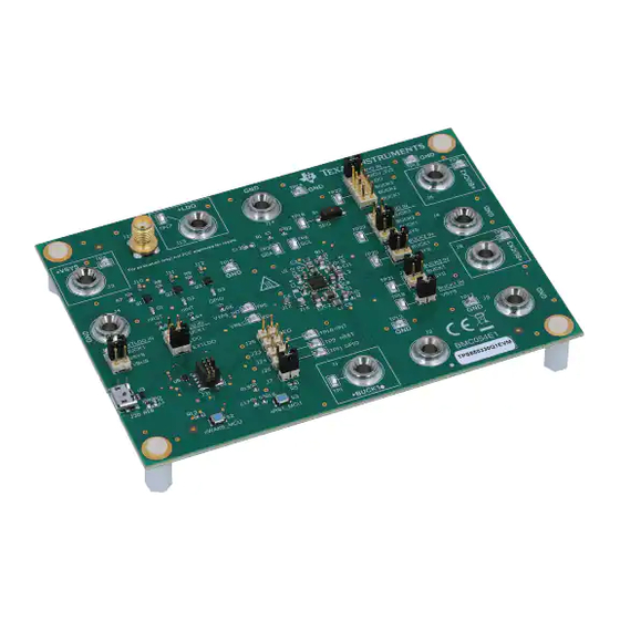
The following sections outline how to configure the TPS650330-Q1 EVM for general experimentation. Figure 4-1. TPS650330-Q1 EVM Top View TPS650330-Q1 EVM User's Guide SLVUBI2A – JULY 2018 – REVISED OCTOBER 2020 Submit Document Feedback Copyright © 2020 Texas Instruments Incorporated... -
Page 7: Test Points
TP18 Buck 1 Input TP19 TP20 TP21 USBD_N TP22 TP23 TP24 VSYS TP25 TP26 TP27 TP28 TP29 USBD_P TP30 SLVUBI2A – JULY 2018 – REVISED OCTOBER 2020 TPS650330-Q1 EVM User's Guide Submit Document Feedback Copyright © 2020 Texas Instruments Incorporated... -
Page 8: Graphical User Interface
, or Linux ® 6.1 TPS650330-Q1 EVM Debugging Refer to Figure 6-1 to debug potential issues while using the TPS650330-Q1 EVM. TPS650330-Q1 EVM User's Guide SLVUBI2A – JULY 2018 – REVISED OCTOBER 2020 Submit Document Feedback Copyright © 2020 Texas Instruments Incorporated... -
Page 9: Figure 6-1. Tps650330-Q1 Evm Debugging Flow
Graphical User Interface Figure 6-1. TPS650330-Q1 EVM Debugging Flow Chart SLVUBI2A – JULY 2018 – REVISED OCTOBER 2020 TPS650330-Q1 EVM User's Guide Submit Document Feedback Copyright © 2020 Texas Instruments Incorporated... -
Page 10: Figure 6-2. Opening Serial Port Options
The GUI contains the following five sections, selectable on the left side of the GUI or by clicking the Menu tab in the top left corner. TPS650330-Q1 EVM User's Guide SLVUBI2A – JULY 2018 – REVISED OCTOBER 2020 Submit Document Feedback Copyright © 2020 Texas Instruments Incorporated... -
Page 11: Figure 6-4. Tps6503Xx-Q1 Gui Home Screen
The Block Diagram section displays the typical components and functional blocks of the PMIC. A block diagram for the Programming BoosterPack is also shown. SLVUBI2A – JULY 2018 – REVISED OCTOBER 2020 TPS650330-Q1 EVM User's Guide Submit Document Feedback Copyright © 2020 Texas Instruments Incorporated... -
Page 12: Figure 6-5. Tps6503Xx-Q1 Gui Block Diagram Page
This register page can poll the device periodically using the Auto Read feature in the top right corner, or allow manual read instructions using the Read Register and Read All Registers buttons. TPS650330-Q1 EVM User's Guide SLVUBI2A – JULY 2018 – REVISED OCTOBER 2020 Submit Document Feedback Copyright © 2020 Texas Instruments Incorporated... -
Page 13: Figure 6-7. Tps6503Xx-Q1 Gui Device Configuration Page
Register Map page, the Device Configuration page can be used to quickly define desired OTP register settings. SLVUBI2A – JULY 2018 – REVISED OCTOBER 2020 TPS650330-Q1 EVM User's Guide Submit Document Feedback Copyright © 2020 Texas Instruments Incorporated... -
Page 14: Figure 6-8. Device Selection For Generating Nvm
TI recommends to set Power On Bit unmasked for each rail that is required in the application. TPS650330-Q1 EVM User's Guide SLVUBI2A – JULY 2018 – REVISED OCTOBER 2020 Submit Document Feedback Copyright © 2020 Texas Instruments Incorporated... -
Page 15: Figure 6-10. Sequencing Overview Tab
For example, if a regulator is enabled but fails to power-up within 200 ms, the sequence settings are not valid. SLVUBI2A – JULY 2018 – REVISED OCTOBER 2020 TPS650330-Q1 EVM User's Guide Submit Document Feedback Copyright © 2020 Texas Instruments Incorporated... -
Page 16: Figure 6-12. Gui Generated Timing Diagram
PMIC will automatically restart with the latest settings. The device can be re-programmed multiple times to evaluate various configurations. Figure 6-13. TPS6503xx-Q1 GUI Re-Program PMIC Page TPS650330-Q1 EVM User's Guide SLVUBI2A – JULY 2018 – REVISED OCTOBER 2020 Submit Document Feedback Copyright © 2020 Texas Instruments Incorporated... -
Page 17: Figure 6-14. Gui Configuration Crc Script
Figure 6-14. GUI Configuration CRC Script 9. Burn the final PMIC register settings to EEPROM. 10.Validate the settings on subsequent startups. SLVUBI2A – JULY 2018 – REVISED OCTOBER 2020 TPS650330-Q1 EVM User's Guide Submit Document Feedback Copyright © 2020 Texas Instruments Incorporated... -
Page 18: Typical Performance Plots
VOUT = 1.2 V IOUT = 1 mA to 300 mA in 1 µs Figure 7-5. Buck 3 Load Transient TPS650330-Q1 EVM User's Guide SLVUBI2A – JULY 2018 – REVISED OCTOBER 2020 Submit Document Feedback Copyright © 2020 Texas Instruments Incorporated... - Page 19 7.4 Efficiency Plots VIN = 9 V VOUT = 3.3 V Ta = 25°C Figure 7-9. Buck 1 Efficiency Curve SLVUBI2A – JULY 2018 – REVISED OCTOBER 2020 TPS650330-Q1 EVM User's Guide Submit Document Feedback Copyright © 2020 Texas Instruments Incorporated...
- Page 20 7.5 LDO Output Noise VIN = 3.3 V VOUT = 2.8 V IOUT = 300 mA Figure 7-12. LDO Output Noise Density TPS650330-Q1 EVM User's Guide SLVUBI2A – JULY 2018 – REVISED OCTOBER 2020 Submit Document Feedback Copyright © 2020 Texas Instruments Incorporated...
-
Page 21: Tps650330-Q1 Evm Schematic
TPS650330-Q1 EVM Schematic 8 TPS650330-Q1 EVM Schematic Figure 8-1. TPS650330-Q1 Schematic SLVUBI2A – JULY 2018 – REVISED OCTOBER 2020 TPS650330-Q1 EVM User's Guide Submit Document Feedback Copyright © 2020 Texas Instruments Incorporated... -
Page 22: Figure 8-2. Msp432E401Y Schematic
TPS650330-Q1 EVM Schematic www.ti.com Figure 8-2. MSP432E401Y Schematic TPS650330-Q1 EVM User's Guide SLVUBI2A – JULY 2018 – REVISED OCTOBER 2020 Submit Document Feedback Copyright © 2020 Texas Instruments Incorporated... -
Page 23: Tps650330-Q1 Evm Pcb Layers
TPS650330-Q1 EVM PCB Layers 9 TPS650330-Q1 EVM PCB Layers Figure 9-1. Top Layer SLVUBI2A – JULY 2018 – REVISED OCTOBER 2020 TPS650330-Q1 EVM User's Guide Submit Document Feedback Copyright © 2020 Texas Instruments Incorporated... -
Page 24: Figure 9-2. Mid-Layer 1
TPS650330-Q1 EVM PCB Layers www.ti.com Figure 9-2. Mid-Layer 1 TPS650330-Q1 EVM User's Guide SLVUBI2A – JULY 2018 – REVISED OCTOBER 2020 Submit Document Feedback Copyright © 2020 Texas Instruments Incorporated... -
Page 25: Figure 9-3. Mid-Layer 2
TPS650330-Q1 EVM PCB Layers Figure 9-3. Mid-Layer 2 SLVUBI2A – JULY 2018 – REVISED OCTOBER 2020 TPS650330-Q1 EVM User's Guide Submit Document Feedback Copyright © 2020 Texas Instruments Incorporated... -
Page 26: Figure 9-4. Mid-Layer 3
TPS650330-Q1 EVM PCB Layers www.ti.com Figure 9-4. Mid-Layer 3 TPS650330-Q1 EVM User's Guide SLVUBI2A – JULY 2018 – REVISED OCTOBER 2020 Submit Document Feedback Copyright © 2020 Texas Instruments Incorporated... -
Page 27: Figure 9-5. Mid-Layer 4
TPS650330-Q1 EVM PCB Layers Figure 9-5. Mid-Layer 4 SLVUBI2A – JULY 2018 – REVISED OCTOBER 2020 TPS650330-Q1 EVM User's Guide Submit Document Feedback Copyright © 2020 Texas Instruments Incorporated... -
Page 28: Figure 9-6. Bottom Layer (Mirrored)
TPS650330-Q1 EVM PCB Layers www.ti.com Figure 9-6. Bottom Layer (Mirrored) TPS650330-Q1 EVM User's Guide SLVUBI2A – JULY 2018 – REVISED OCTOBER 2020 Submit Document Feedback Copyright © 2020 Texas Instruments Incorporated... -
Page 29: Tps650330-Q1 Evm Bill Of Materials
J25, J26, J27, J15, J16 Header, 100 mil, 2x2, Tin, TH Header, 2x2, 2.54 PEC02DAAN Sullins mm, TH Connector Solutions SLVUBI2A – JULY 2018 – REVISED OCTOBER 2020 TPS650330-Q1 EVM User's Guide Submit Document Feedback Copyright © 2020 Texas Instruments Incorporated... - Page 30 Q200 Grade 0, 0402 S1, S4 Switch, Slide, SPDT, On-Off-On, 9.5x5 mm AS1E-2M-10-Z Copal 3 Pos, 0.05 A, 48 V, TH Electronics TPS650330-Q1 EVM User's Guide SLVUBI2A – JULY 2018 – REVISED OCTOBER 2020 Submit Document Feedback Copyright © 2020 Texas Instruments Incorporated...
- Page 31 1 µF CAP, CERM, 1 µF, 10 V, ± 10%, 0603 LMK107B7105KAHT Taiyo Yuden X7R, AEC-Q200 Grade 1, 0603 SLVUBI2A – JULY 2018 – REVISED OCTOBER 2020 TPS650330-Q1 EVM User's Guide Submit Document Feedback Copyright © 2020 Texas Instruments Incorporated...
-
Page 32: Tps650330-Q1 Silicon Revision Changes
BUCK1, BUCK2, BUCK3, and the LDO. Status bits also added for nRSTOUT, GPIO, and SEQ pins TPS650330-Q1 EVM User's Guide SLVUBI2A – JULY 2018 – REVISED OCTOBER 2020 Submit Document Feedback Copyright © 2020 Texas Instruments Incorporated... -
Page 33: Revision History
Added the TPS650330-Q1 EVM PCB Layers section..................• Added the TPS650330-Q1 EVM Bill of Materials section.................29 • Added the TPS650330-Q1 Silicon Revision Changes section................. SLVUBI2A – JULY 2018 – REVISED OCTOBER 2020 TPS650330-Q1 EVM User's Guide Submit Document Feedback Copyright © 2020 Texas Instruments Incorporated... - Page 34 STANDARD TERMS FOR EVALUATION MODULES Delivery: TI delivers TI evaluation boards, kits, or modules, including any accompanying demonstration software, components, and/or documentation which may be provided together or separately (collectively, an “EVM” or “EVMs”) to the User (“User”) in accordance with the terms set forth herein.
- Page 35 www.ti.com Regulatory Notices: 3.1 United States 3.1.1 Notice applicable to EVMs not FCC-Approved: FCC NOTICE: This kit is designed to allow product developers to evaluate electronic components, circuitry, or software associated with the kit to determine whether to incorporate such items in a finished product and software developers to write software applications for use with the end product.
- Page 36 www.ti.com Concernant les EVMs avec antennes détachables Conformément à la réglementation d'Industrie Canada, le présent émetteur radio peut fonctionner avec une antenne d'un type et d'un gain maximal (ou inférieur) approuvé pour l'émetteur par Industrie Canada. Dans le but de réduire les risques de brouillage radioélectrique à...
- Page 37 www.ti.com EVM Use Restrictions and Warnings: 4.1 EVMS ARE NOT FOR USE IN FUNCTIONAL SAFETY AND/OR SAFETY CRITICAL EVALUATIONS, INCLUDING BUT NOT LIMITED TO EVALUATIONS OF LIFE SUPPORT APPLICATIONS. 4.2 User must read and apply the user guide and other available documentation provided by TI regarding the EVM prior to handling or using the EVM, including without limitation any warning or restriction notices.
- Page 38 Notwithstanding the foregoing, any judgment may be enforced in any United States or foreign court, and TI may seek injunctive relief in any United States or foreign court. Mailing Address: Texas Instruments, Post Office Box 655303, Dallas, Texas 75265 Copyright © 2019, Texas Instruments Incorporated...
- Page 39 TI products. TI’s provision of these resources does not expand or otherwise alter TI’s applicable warranties or warranty disclaimers for TI products.IMPORTANT NOTICE Mailing Address: Texas Instruments, Post Office Box 655303, Dallas, Texas 75265 Copyright © 2021, Texas Instruments Incorporated...
Need help?
Do you have a question about the TPS65033-Q1 Series and is the answer not in the manual?
Questions and answers