Advertisement
Quick Links
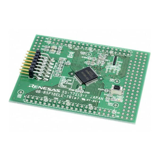
RL78/L13 ターゲット・ボード
QB-R5F10WMG-TB ユーザーズ・マニュアル
本製品は、ルネサス エレクトロニクス製のプログラミング機能付きオンチップ・デバッグ・エミュレータ E1 を使用して、マイコンの動作を試
すためのターゲット・ボードです。
①RL78/L13 ターゲット・ボード(QB-R5F10WMG-TB)の特徴
●RL78/L13(R5F10WMG)搭載
●20MHz と 32.768kHz の発振子を搭載
●ユニバーサル・エリア(2.54mm ピッチ)を搭載
●フラッシュ・メモリ・プログラミング、オンチップ・デバッグに両対応(TOOL0 端子使用)
●マイコンの端子を周辺ボード・コネクタに配置した高拡張性
●鉛(Pb)フリー対応品
②ハードウエア仕様
CPU R5F10WMG
メイン・クロック動作周波数
搭載部品
CN1,CN4, CN5: 周辺ボードコネクタ(2.54mm ピッチ) 20pin ソケット(パッドのみ)
CN2: 周辺ボードコネクタ(2.54mm ピッチ) 15pin ソケット x2(パッドのみ)
CN3: 14pin コネクタ(E1 接続用)
Power LED: 赤 x1(LED3)
評価用 LED: 黄 x2(LED1 は P41,LED2 は P42 へ接続)
評価用 SW: SW1(INTP0 へ接続)
メイン・クロック(OSC1): 20MHz 発振子(X1,X2 へ接続)
サブ・クロック(OSC2): 32.768kHz 発振子(XT1,XT2 へ接続)
動作電圧
2.7V~5.5V(OSC1:20MHz 発振子使用時)
③寸法、部品配置など
LCD駆動設定
メインクロック
LED2
P42
29
評価用LED
30
上:LED2
LED1
P41
VDD VL3 VL2 VL1 GND CAPH
VL4 VL3 VL2 VL1
下:LED1
LED3
13
Power LED
CN5:SEG50-SEG35
1
CN4:SEG34-SEG16
CN1:SEG15-COM0
14pin コネクタ
VDD
CN5
CN4
CN1
基板上のパターン
について:パターンをカットすることで、その回路はオープンとなります。
再度接続させたい場合は半田ショートしてください。
P41,P42 を使用する場合は LED の右のショートパッドをパターンカットしてください。
回路図のパッドの表示
オープン:
ショート:
④使用上の注意
・本製品に関してのサポートはお受けしておりません。初期不良の場合に限り、交換いたします。
R20UT2199XJ0300 Rev.3.00
2013.06.24
ユーザーズ・マニュアル
R20UT2199XJ0300
Rev3.00 2013.06.24
20MHz(ボード上の発振子を使う場合)
サブクロック
1
2
CN2
20
10
CN2
P137
CAPL
SW1(INTP0)
SW1
RL78
/L13
ユニバーサルエリア
QB-R5F10WMG-TB(e) SS-77220
N.C.
CN1,CN4, CN5
71.12mm
RL78/L13 Target board
QB-R5F10WMG-TB User's Manual
The QB- R5F10WMG -TB is a target board used for evaluating microcontroller operations, using the E1, the Renesas Electronics
on-chip debug emulator with programming function (hereinafter referred to as E1).
(1) RL78/L13 target board (QB-R5F10WMG-TB) features
● Incorporates RL78/L13 (R5F10WMG).
● A 20 MHz resonator and a 32.768 kHz resonator are mounted.
● Equipped with universal area (2.54 mm pitch)
● Supports both flash memory programming and on-chip debugging (using TOOL0 pin)
● Highly extendable; peripheral board connectors are equipped with microcontroller pins
● Lead-free (Pb-free) product
(2) hardware specifications
CPU R5F10WMG
Main clock operating frequency
Embedded parts
CN1, CN4, CN5: Peripheral board connectors (2.54 mm pitch), 20-pin socket (pad only)
CN2: Peripheral board connectors (2.54 mm pitch), 15-pin socket 2 (pad only)
CN3: 14-pin connector (for E1 connection)
Power LED: Red 1 (LED3)
Test LED: Yellow 2 (LED1 connected to P41, LED2 connected to P42)
Test SW: SW1 (connected to INTP0)
Main clock (OSC1): 20 MHz resonator(connected to X1 and X2)
Sub clock (OSC2): 32.768 KHz resonator (connected to XT1 and XT2)
Operating voltage
2.7 to 5.5 V(when 20MHz resonator used at OSC1)
(3) Dimensions and parts layout
LCD driver pattern
Test LED
upper:LED2
lower:LED1
Power LED
14pin connector
Splitting this wiring leaves open the relevant circuit (
Pattern on the board:
To reconnect the circuit, short the circuit by soldering (
When using P41 and P42, cut off the short pad on the right side of LED.
Showing of the pad on circuit diagram. open:
(4) Notes on use
● Renesas Electronics will not provide any support for this board, but the board can be exchanged with a new product only when
it has an initial failure.
Page 1 of 3
R20UT2199XJ0300 Rev.3.00
2013.06.24
20 MHz. (when use resonator mounted on board)
Main Clock
LED2
P42
29
30
20
CN2
LED1
P41
10
VDD VL3 VL2 VL1 GND CAPH
VL4 VL3 VL2 VL1
CAPL
LED3
13
RL78
/L13
1
QB-R5F10WMG-TB(PROTO TYPE)
CN5(TOP) CN4 CN1(BOTTOM)
VDD
CN5
CN4
CN1
71.12mm
short:
User's Manual
R20UT2199XJ0300
Rev 3.00 2013.06.24
Sub Clock
1
2
CN2
P137
SW1(INTP0)
SW1
Universal area
CN1, CN4, CN5
).
).
Page 1 of 3
Advertisement

Subscribe to Our Youtube Channel
Related Manuals for Renesas QB-R5F10WMG-TB


Summary of Contents for Renesas QB-R5F10WMG-TB
- Page 1 オープン: ショート: (4) Notes on use ④使用上の注意 ● Renesas Electronics will not provide any support for this board, but the board can be exchanged with a new product only when ・本製品に関してのサポートはお受けしておりません。初期不良の場合に限り、交換いたします。 it has an initial failure. R20UT2199XJ0300 Rev.3.00 Page 1 of 3 R20UT2199XJ0300 Rev.3.00...
- Page 2 ユーザーズ・マニュアル User’s Manual R20UT2199XJ0300 R20UT2199XJ0300 RL78/L13 ターゲット・ボード RL78/L13 Target board Rev3.00 2013.06.24 QB-R5F10WMG-TB User’s Manual Rev 3.00 2012.06.24 QB-R5F10WMG-TB ユーザーズ・マニュアル クロック, ポートの設定方法 Setting of Clock and port. - Setting of main clock ○メインクロックの設定 OSC1 pad OSC3 pad (back of board)
- Page 3 AVREFP AVREFP AVREFM AVREFM SEG15 SEG34 0.1uF 0.1uF SEG14 SEG33 SEG13 SEG32 SEG12 SEG31 SEG11 SEG30 SEG50 SEG10 SEG29 SEG49 1.6Kohm 1.6Kohm 1.6Kohm 1.6Kohm 1.6Kohm 1.6Kohm SEG9 SEG28 SEG48 SEG8 SEG27 SEG47 SEG7 SEG26 SEG46 SEG6 SEG45 SEG5 SEG25 SEG44 SEG4 SEG24 SEG43...
Need help?
Do you have a question about the QB-R5F10WMG-TB and is the answer not in the manual?
Questions and answers