
Related Manuals for Measurement Computing PCIM-DDA06/16


Summary of Contents for Measurement Computing PCIM-DDA06/16
- Page 1 PCIM-DDA06/16 Analog Output and Digital I/O User's Guide January 2019. Rev 9 © Measurement Computing Corporation...
- Page 2 Other product and company names mentioned herein are trademarks or trade names of their respective companies. © 2019 Measurement Computing Corporation. All rights reserved. No part of this publication may be reproduced, stored in a retrieval system, or transmitted, in any form by any means, electronic, mechanical, by photocopying, recording, or otherwise without the prior written permission of Measurement Computing Corporation.
-
Page 3: Table Of Contents
What you will learn from this user's guide ......................4 Conventions in this user's guide ......................... 4 Where to find more information ......................... 4 Chapter 1 Introducing the PCIM-DDA06/16 ......................5 Functional block diagram ........................... 5 Chapter 2 Installing the PCIM-DDA06/16 ......................6 Unpacking................................ -
Page 4: Preface
Preface About this User's Guide What you will learn from this user's guide This user's guide describes the Measurement Computing PCIM-DDA06/16 data acquisition device and lists device specifications. Conventions in this user's guide For more information Text presented in a box signifies additional information and helpful hints related to the subject matter you are reading. -
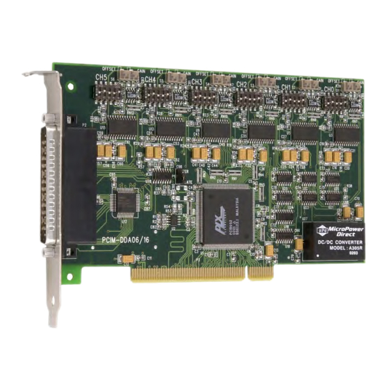
Page 5: Introducing The Pcim-Dda06/16
The PCIM-DDA06/16 digital I/O lines are a direct interface to an 82C55. The 82C55 is a CMOS chip with TTL level inputs and outputs. The 8255 can source or sink about 2.5 mA. This is enough to switch other TTL or similar inputs, but is inadequate to drive relays, LEDs or solid-state relays without additional buffering. -
Page 6: Installing The Pcim-Dda06/16
Install the software before you install your device The driver needed to run the PCIM-DDA06/16 is installed with the software. Therefore, you need to install the software package you plan to use before you install the hardware. -
Page 7: Analog Output Range Switch
DAC control register address (any of the addresses BADR3 + 0 to BADR3 + B) is read In this way, the PCIM-DDA06/16 can be set to hold new values until all channels are loaded, then update all six channels simultaneously. This is a very useful feature for multi-axis motor control. -
Page 8: Signal Connections
PCIM-DDA06/16 User's Guide Installing the PCIM-DDA06/16 If your board has been powered-off for more than 10 minutes, allow your computer to warm up for at least 15 minutes before acquiring outputting analog data with this board. This warm-up period is required for the board to achieve its rated accuracy. -
Page 9: Cabling
PCIM-DDA06/16 User's Guide Installing the PCIM-DDA06/16 The analog outputs of the PCIM-DDA06/16 are two-wire hook-ups. Always use analog ground (LLGND) as the ground reference for all analog hook-ups. Cabling Figure 5. C37FF-x cable Figure 6. C37FFS-x cable Field wiring, signal termination, and conditioning You can use the following cabling, screw termination, and signal conditioning products with the PCIM- DDA06/16. -
Page 10: Chapter 3 Specifications
±1.0 LSB max, ±0.5 LSB typ Each PCIM-DDA06/16 is tested at the factory to assure the board’s overall error does not exceed ±2.0 LSB. Total board error is a combination of gain, offset, integral linearity and differential linearity error. The theoretical worst-case error of the board may be calculated by summing these component errors. -
Page 11: Analog Output Drift
PCIM-DDA06/16 User's Guide Specifications Analog output drift Table 3. Worst case analog output drift specifications Range Gain Drift (LSB/°C) Offset Drift (LSB/°C) Overall Drift (LSB/°C) ±10.0 V ±5.00 V 0 V to 10.0 V 0 V to 5.0 V Digital I/O Table 4. -
Page 12: Signal Connector
PCIM-DDA06/16 User's Guide Specifications Signal connector Table 8. Signal connector specifications Parameter Specification Connector type 37-pin male D connector Compatibility Pinout identical to CIO-DDA06/16 Compatible cables C37FF-x C37FFS-x DFCON-37 (D-connector, D-shell, and termination pins to construct your own cable) Compatible accessory products with the C37FF-x... -
Page 13: Eu Declaration Of Conformity
December 4, 2017, Norton, Massachusetts USA Test Report Number: EMI5259.09 Measurement Computing Corporation declares under sole responsibility that the product PCIM-DDA06/16 is in conformity with the relevant Union Harmonization Legislation and complies with the essential requirements of the following applicable European Directives:... - Page 14 Measurement Computing Corporation NI Hungary Kft 10 Commerce Way H-4031 Debrecen, Hátar út 1/A, Hungary Norton, Massachusetts 02766 Phone: +36 (52) 515400 (508) 946-5100 Fax: +36 (52) 515414 Fax: (508) 946-9500 http://hungary.ni.com/debrecen E-mail: info@mccdaq.com www.mccdaq.com...
Need help?
Do you have a question about the PCIM-DDA06/16 and is the answer not in the manual?
Questions and answers