
Related Manuals for Tait T880 II Series


Summary of Contents for Tait T880 II Series
- Page 1 M880-00 T880 Series II Base Station Equipment 800-960MHz Initial Adjustment Manual August 2000 M880-00-2A0 Copyright TEL 10/07/00...
- Page 2 Toll Free: 1 800 077 112 Fax: 61 7 3865 7990 Fax: 64 3 343 0558 http:/ /www.taitworld.com Beijing Singapore Tait Electronics (Far East) Pte Ltd Tait Mobile Radio (HK) Ltd 4 Leng Kee Road Beijing Representative Office SIS Building #05-11A Room 610, Tower 2...
- Page 3 Tait Electronics Ltd. Ordering Tait Service Manuals You can order additional copies of this manual from your nearest Tait Dealer or Cus- tomer Service Organisation. When ordering, make sure you quote the correct Tait prod- uct code ("M"...
- Page 4 M880-00 Table Of Contents This manual is divided into five parts as listed below, with each part being further sub- divided into sections. There is a detailed table of contents at the start of each part and/ or section. Part Title Introduction To Servicing T885 Receiver...
-
Page 5: Table Of Contents
M880-00 Part A Introduction To Servicing This part of the manual is divided into the sections listed below. These sections provide some general and advisory information on servicing procedures, and a brief history of PGM800Win programming software. Section Title Page General Additional Technical Information Caution: CMOS Devices... - Page 6 M880-00 10/07/00 Copyright TEL...
-
Page 7: General
If you have any questions about this manual or the equipment it describes, please con- tact your nearest Tait Dealer or Customer Service Organisation. If necessary, you can get additional technical help from Customer Support, Radio Systems Division, Tait Elec- tronics Ltd, Christchurch, New Zealand (full contact details are on page 2). -
Page 8: Caution: Aerial Load
A1.2 General M880-00 conductive conductive rubber wrist strap bench mat to building earth (not mains earth) Figure 1.2 Typical Anti-static Bench Set-up Caution: Aerial Load The equipment has been designed to operate safely under a wide range of aerial loading conditions. -
Page 9: Mechanical
Mechanical A2.1 M880-00 Mechanical Torx Recess Head Screws Torx recess head screws are becoming the standard screw head type in all T800 Series II equipment, with Pozidriv and Philips recess head screws being used in fewer applica- tions. The Torx recess head has the advantage of improved screwdriver tip location, reducing the chances of screw head damage caused by the driver tip rotating within the recess. -
Page 10: Pozidriv & Philips Recess Head Screws
A2.2 Mechanical M880-00 Pozidriv & Philips Recess Head Screws Pozidriv and Philips recess head screws will continue to be used in T800 Series II equip- ment in a few special applications. It is important that you use the correct type and size screwdriver for each screw type to avoid damaging the screw head. -
Page 11: Disassembly/Reassembly
Mechanical A2.3 M880-00 Disassembly/Reassembly 2.3.1 Receivers/Transmitters To carry out alignment or change option links, you need to remove only the top cover, i.e. the one adjacent to the front panel handle and on the opposite side to the main D-range connector (D-range 1/PL100). You need to remove the bottom cover to: •... -
Page 12: Cover Screw Torques
A2.4 Mechanical M880-00 Cover Screw Torques Receivers/Transmitters .. 2.0Nm/18in.lbf. Power Amplifiers .. 0.9Nm/8in.lbf. To ensure that the receiver and transmitter will continue to meet their per- Note: formance specifications, you must tighten the screws securing the bottom cover (the one furthest from the handle) to the correct torque, and in the cor- rect order, as shown below. -
Page 13: Chassis & Cover Compatibility
Mechanical A2.5 M880-00 Chassis & Cover Compatibility The chassis and covers used in T800 Series II modules incorporate a number of design changes to improve Electro-Magnetic Compatibility (EMC) performance. It is impor- tant that only the new-design covers are fitted to the new chassis to ensure correct mechanical fit and continued compliance with appropriate EMC Type Approval regula- tions. - Page 14 A2.6 Mechanical M880-00 10/07/00 Copyright TEL...
-
Page 15: Component Replacement
Component Replacement A3.1 M880-00 Component Replacement Leaded Components Whenever you are doing any work on the PCB that involves removing or fitting compo- nents, you must take care not to damage the copper tracks. The two satisfactory meth- ods of removing components from plated-through hole (PTH) PCBs are detailed below. Note: The first method requires the use of a desoldering station, e.g. -
Page 16: Surface Mount Devices
Tait Dealer or Customer Service Organisa- tion equipped with the necessary facilities. Repairs attempted with incorrect equipment or by untrained personnel may result in perma- nent damage. If in doubt, contact your nearest Tait Dealer or Customer Service Organisation. Cased Mica Capacitors... -
Page 17: Software History
Software History A4.1 M880-00 Software History 28/06/96 PGM800Win Version 1.0 18/08/97 PGM800Win Version 2.00 PGM800Win V1.0 PGM800Win V1.0 is different in concept from DOS versions of PGM800 in that it is Win- dows based. It also includes many new and improved features over DOS versions of PGM800. - Page 18 A4.2 Software History M880-00 • Extra information that is not stored in the radio (but which is still relevant to the radio) can be saved to a file on disk (e.g. note field, auxiliary pin names, etc.). Note: The data files produced by BASEPROG V1.0, all DOS versions of PGM800, and PGM800Win V1.0 are still compatible with PGM800Win V2.00.
- Page 19 M880-00 Part B T885 Receiver This part of the manual is divided into six sections, as listed below. There is a detailed table of contents at the start of each section. Section Title General Information Circuit Operation Initial Tuning & Adjustment Functional Testing (not available for Initial Adjustment manual) Fault Finding (not available for Initial Adjustment manual) PCB Information...
- Page 20 M880-00 10/07/00 Copyright TEL...
- Page 21 T885 General Information B1.1 M880-00 T885 General Information This section provides a brief description of the T885 receiver, along with detailed speci- fications and a list of types available. The following topics are covered in this section. Section Title Page Introduction Specifications 1.2.1...
-
Page 22: T885 General Information B1.1
B1.2 T885 General Information M880-00 10/07/00 Copyright TEL... -
Page 23: T885 General Information
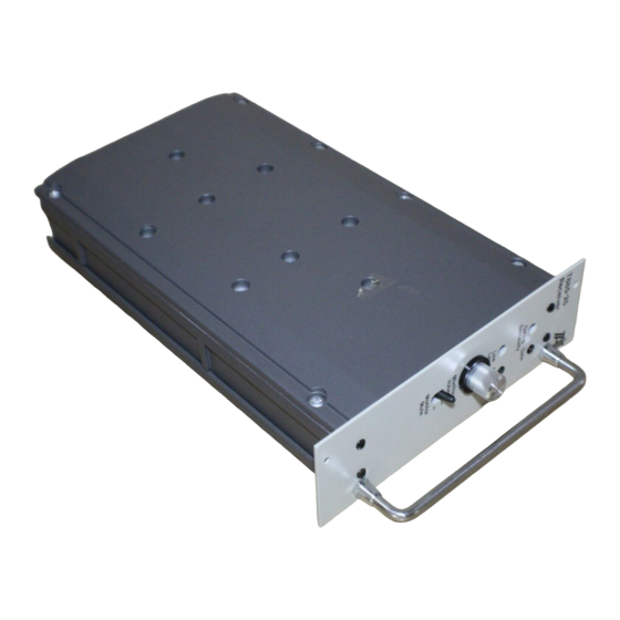
The front panel controls include gating sensitivity, line level, monitor volume and a monitor mute switch. The T885 has a width of 60mm and occupies a single space in a Tait rack frame, which has the ability to accommodate up to seven standard modules. -
Page 24: Specifications
Details of test methods and the conditions which apply for Type Approval testing in all countries can be obtained from Tait Electronics Ltd. The terms "wide bandwidth" and "narrow bandwidth" used in this and following sec- tions are defined in the following table. -
Page 25: General
1.4) .. ±1.5ppm, -30°C to +60°C Signal Strength Indicator .. -115dBm to -70dBm, 0 to 5V (RSSI optional) at approx. 10dB/V 1. Additional channels may be factory programmed. Contact your nearest Tait Dealer or Customer Service Organisation. Copyright TEL 10/07/00... - Page 26 B1.6 T885 General Information M880-00 IF Amplifiers: Frequencies .. 45MHz and 455kHz Bandwidths- Narrow Bandwidth (NB) .. 7.5kHz Wide Bandwidth (WB) .. 15kHz Sensitivity (De-emphasised Response): Single Channel .. -117dBm Bandspread (12dB Sinad) .. -115dBm (across switching range) Sensitivity (Flat Response): Single Channel ..
-
Page 27: Audio Section
T885 General Information B1.7 M880-00 1.2.4 Audio Section 1.2.4.1 General Outputs Available .. line and monitor Frequency Response .. flat or de-emphasised (750µs) (link selectable) Flat Response: Bandwidth .. 67 to 3400Hz Response .. within +1, -2dB of output level at 1kHz De-emphasised Response: Bandwidth... -
Page 28: Mute Operation
B1.8 T885 General Information M880-00 1.2.4.3 Mute Operation Systems Available .. noise mute and carrier mute Noise Mute: Operating Range .. 6-20dB sinad Hysteresis .. 1.5 to 6dB Threshold .. adjustable to -105dBm Opening Time .. 20ms Closing Time .. 50ms Carrier Mute (Optional): Operating Range .. -
Page 29: Telecommunications Industry Association
T885 General Information B1.9 M880-00 1.2.6.2 Telecommunications Industry Association ANSI/TIA/EIA-603-1992 Land mobile FM or PM communications equipment measurement and performance standards. Copyright TEL 10/07/00... -
Page 30: Product Codes
The following explanation of T880 Series II product codes is not intended to suggest that any combination of features is necessarily available in any one product. Consult your nearest Tait Dealer or Customer Service Organisation for more information regarding the availability of specific models, types and options. -
Page 31: Standard Product Range
Standard Product Range The following table lists the range of standard T885 types (i.e. no options fitted) availa- ble at the time this manual was published. Consult your nearest Tait Dealer or Cus- tomer Service Organisation for more information. Frequency Range (MHz) - Page 32 B1.12 T885 General Information M880-00 10/07/00 Copyright TEL...
- Page 33 T885 Circuit Operation B2.1 M880-00 T885 Circuit Operation This section provides a basic description of the circuit operation of the T885 receiver. Note: Unless otherwise specified, the term "PGM800Win" used in this and follow- ing sections refers to version 2.00 and later of the software. Refer to Section 6 where the parts lists, grid reference index and diagrams will provide detailed information on identifying and locating components and test points on the main PCB.
- Page 34 B2.2 T885 Circuit Operation M880-00 10/07/00 Copyright TEL...
-
Page 35: T885 Circuit Operation
T885 Circuit Operation B2.3 M880-00 Introduction Noise Mute Mixer Mixer Speaker Front 45MHz 455kHz Limiter/ Audio Detector Processor 600W Line Synthesised Second Local Local Oscillator Oscillator Carrier Mute 12.8MHz Master Oscillator RSSI Figure 2.1 T885 High Level Block Diagram The T885 receiver consists of a number of distinct stages: •... -
Page 36: Receiver Front End
B2.4 T885 Circuit Operation M880-00 Receiver Front End (Refer to the front end, IF section and audio processor circuit diagrams (sheets 4, 3 and 2 respectively) in Section 6.2.) Local Oscillator (From Synthesiser) RF In 800-960MHz 3dB Pad Post 4-Pole Harmonic Helical Helical... -
Page 37: Mixer
T885 Circuit Operation B2.5 M880-00 Mixer (Refer to the front end circuit diagram (sheet 4) in Section 6.2 and Figure 2.2.) IC410 is a high level mixer requiring a local oscillator (LO) drive level of +17dBm (nom- inal). The voltage controlled oscillator (VCO) generates a level of +20dBm (typical) and this is fed to the mixer via a 3dB attenuator pad. -
Page 38: Noise Mute (Squelch)
B2.6 T885 Circuit Operation M880-00 Noise Mute (Squelch) (Refer to the audio processor and IF section circuit diagrams (sheets 2 and 3 respec- tively) in Section 6.2 and Figure 2.2.) The noise mute operates on the detected noise outside the audio bandwidth. Two oper- ational amplifiers in IC330 are used as an active band-pass filter centred on 70kHz to fil- ter out audio components and provide gain. -
Page 39: Audio Processor
T885 Circuit Operation B2.7 M880-00 Audio Processor (Refer to the audio processor circuit diagram (sheet 2) in Section 6.2.) From RSSI RSSI Output RSSI IF Stage (Optional) PL270 Mute Relay Relay PL250 Carrier Mute Gate Output Noise Mute Rx Disable Rx Disable Timer (Optional Pad) -
Page 40: Power Supply And Regulators
B2.8 T885 Circuit Operation M880-00 The audio can also be disabled using the "RX-DISABLE" inputs, pads 225 or 228, having connected the "RX-DISABLE" link between pins 1 & 2 of PL260. An adjustable time delay (RV220) is provided on these lines. In order to disable the audio, either pad must be pulled to 0V. -
Page 41: Microcontroller
T885 Circuit Operation B2.9 M880-00 Microcontroller (Refer to the microcontroller circuit diagram (sheet 8) in Section 6.2.) 5V Digital Watchdog Timer Regulator & LVI Reset Watchdog Microcontroller Cavity Channel Select Port 12.8MHz Microcontroller Clock Auxiliary Output Port External Serial Converter Port Audio In CTCSS... -
Page 42: Synthesised Local Oscillator
B2.10 T885 Circuit Operation M880-00 2.10 Synthesised Local Oscillator (Refer to the synthesiser circuit diagram (sheet 7) and the VCO circuit diagram (sheet 5) in Section 6.2.) FREQUENCY SYNTHESISER IC VCO PCB Reference Phase Charge Loop Output Divider Detector Pump Filter Buffer Buffer... -
Page 43: Vco
T885 Circuit Operation B2.11 M880-00 2.11 (Refer to the VCO circuit diagram (sheet 5) in Section 6.2.) The VCO consists of several stages: oscillator, cascode buffer, broadband amplifier and output buffer. The oscillator transistor (Q504) operates in a common base Colpitts con- figuration and is capacitively coupled to a short-circuited coaxial resonator (&TL500). -
Page 44: T885 Rssi Block Diagram
B2.12 T885 Circuit Operation M880-00 2.12 Received Signal Strength Indicator (RSSI) (Refer to the IF section circuit diagram (sheet 3) in Section 6.2.) The RSSI provides a DC voltage proportional to the signal level at the receiver input and is an on-chip function of the demodulator IC (IC300). Circuitry external to IC300 condi- tions the RSSI signal and the voltage is available at D-range 1 (PL100 pin 5). - Page 45 T885 Initial Tuning & Adjustment B3.1 M880-00 T885 Initial Tuning & Adjustment Caution: This equipment contains CMOS devices which are susceptible to dam- age from static charges. Refer to Section 1.2 in Part A for more infor- mation on anti-static procedures when handling these devices. Note: To ensure that the T885 will continue to meet its performance specifications, you must tighten the bottom cover screws to the correct torque, and in the...
- Page 46 B3.2 T885 Initial Tuning & Adjustment M880-00 Section Title Page 3.4.6 CTCSS 3.4.6.1 Decoder Operation 3.4.6.2 Opening Sinad 3.4.6.3 High Pass Filter 3.4.7 RSSI (If Used) Audio Processor Links 3.5.1 General 3.5.2 Audio Processor Linking Details For CTCSS Synthesiser Alignment 3.10 Alignment Of Receiver Front End And IF 3.10...
-
Page 47: T885 Initial Tuning & Adjustment
PCB. Refer to Part C in the T800 Series Ancillary Equipment Service Manual (M800-00-101 or later issue) or consult your nearest Tait Dealer or Customer Service Organisation for further details. 1. Use the "Read Module" function in PGM800Win to find out what the default channel is. -
Page 48: Test Equipment Required
B3.4 T885 Initial Tuning & Adjustment M880-00 Test Equipment Required You will need the following test equipment: • computer with PGM800Win installed • T800 programming kit • module programming interface (e.g. T800-01-0004 - optional) • 13.8V power supply • digital multimeter •... -
Page 49: Short Tuning Procedure
T885 Initial Tuning & Adjustment B3.5 M880-00 Short Tuning Procedure Use this procedure only if you want to reprogram the receiver to a frequency outside the 6MHz switching range and do not intend to carry out any other major adjustments or repairs. -
Page 50: Mute Adjustment
B3.6 T885 Initial Tuning & Adjustment M880-00 Inject a strong on-channel RF signal with ±3kHz deviation [±1.5kHz] at 1kHz into the antenna socket and adjust the helical resonators (#H900, #H400 and #H401) to give best sinad. Continually decrease the RF level to maintain 12dB sinad. Readjust #H900, #H400 and #H401 to give best sinad. -
Page 51: Ctcss
T885 Initial Tuning & Adjustment B3.7 M880-00 3.4.6 CTCSS 3.4.6.1 Decoder Operation Program a CTCSS tone on the default channel using PGM800Win. Set the RF signal generator output to -70dBm. Modulate the generator with both: • a 1kHz tone at ±3kHz deviation [±1.5kHz] •... -
Page 52: Rssi (If Used)
B3.8 T885 Initial Tuning & Adjustment M880-00 3.4.7 RSSI (If Used) Apply an on-channel signal from the RF generator at a level of -110dBm with ±3kHz deviation [±1.5kHz] at 1kHz. Adjust RV345 (RSSI level) to give 2.0V RSSI output on pin 5 of D-range 1 (PL100) when measured with a high impedance DMM. -
Page 53: Audio Processor Linking Details For Ctcss
T885 Initial Tuning & Adjustment B3.9 M880-00 3.5.2 Audio Processor Linking Details For CTCSS You must connect the audio processor links correctly according to the CTCSS option used, as shown in the table below. CTCSS Option PL230 PL240 standard, no CTCSS 2 - 3 2 - 3 received CTCSS + speech passed to line output... -
Page 54: Synthesiser Alignment
B3.10 T885 Initial Tuning & Adjustment M880-00 Synthesiser Alignment • Ensure that the receiver has been programmed with the required frequencies using the PGM800Win software. • Connect a high impedance voltmeter to the via next to R520 in the VCO cavity (this measures the synthesiser loop voltage). -
Page 55: Gating Delay
T885 Initial Tuning & Adjustment B3.11 M880-00 Trim the synthesiser TCXO (=IC700) for zero beat. Note: If a second oscillator is not available, you can connect a frequency counter to IC710 pin 8 (i.e. after the TCXO buffer) via an oscilloscope probe to measure the TCXO frequency directly (12.8MHz). -
Page 56: Noise Mute Adjustment
B3.12 T885 Initial Tuning & Adjustment M880-00 Noise Mute Adjustment Connect pins 1 & 2 of PL250 to enable the noise mute. Align the receiver as instructed in Section 3.6 Section 3.7. Set the RF level to -105dBm with ±3kHz deviation [±1.5kHz] at 1kHz. Set RV230 (front panel gating sensitivity) fully anticlockwise. -
Page 57: Audio Processor
T885 Initial Tuning & Adjustment B3.13 M880-00 3.12 Audio Processor 3.12.1 Line Amplifier Output Apply an on-channel signal from the RF generator at a level of -70dBm with ±3kHz deviation [±1.5kHz] at 1kHz. Adjust RV210 (front panel line level) to give an output of +10dBm on the 600 ohm line. -
Page 58: High Pass Filter
B3.14 T885 Initial Tuning & Adjustment M880-00 Observe the sinad meter and reduce the RF level until the receiver mute closes. Slowly increase the signal level until the receiver mute just opens and stays open. With PL240 pins 1 & 2 linked (high pass filter bypassed), check that the sinad is less than 6dB. - Page 59 T885 PCB Information B6.1.1 M880-00 T885 PCB Information Caution: This equipment contains CMOS devices which are susceptible to damage from static charges. Refer to Section 1.2 in Part A for more information on anti-static procedures when handling these devices. Note: To ensure that the T885 will continue to meet its performance specifications, you must tighten the bottom cover screws to the correct torque, and in the correct order, as described in...
- Page 60 B6.1.2 T885 PCB Information M880-00 10/07/00 Copyright TEL...
- Page 61 T885 PCB Information B6.1.3 M880-00 Introduction Product Type Identification You can identify the receiver type by checking the product code printed on a label on the rear of the chassis (product codes are explained in Section 1.3 in this Part of the manual, and Figure 1.1 in Part A shows typical labels).
- Page 62 Components without circuit references are listed in IPN order. The number in brackets at the end of each entry refers to the Tait internal Change Order document. IPN of new...
- Page 63 T885 PCB Information B6.1.5 M880-00 Variant Components A variant component is one that has the same circuit reference but different value or specification in different product types. Where two products share the same PCB, the term “variant” is also used to describe components unplaced in one product.
- Page 64 B6.1.6 T885 PCB Information M880-00 Using CAD Circuit Diagrams Reading a CAD circuit diagram is similar to reading a road map, in that both have an alphanumeric border. The circuit diagrams in this manual use letters to represent the horizontal axis, and num- bers for the vertical axis.
- Page 65 T885 PCB Information B6.2.1 M880-00 T885 Receiver PCB This section contains the following information. Section Page 220-01595-02 Parts List 6.2.3 Mechanical & Miscellaneous Parts 6.2.10 Grid Reference Index 6.2.11 PCB Layout - Top Side 6.2.15 PCB Layout - Bottom Side 6.2.16 Receiver Overview Diagram 6.2.17...
- Page 66 B6.2.2 T885 PCB Information M880-00 10/07/00 Copyright TEL...
- Page 67 IPN 220-01595-02 T885 PCB Information B6.2.3 M880-00 T885 Parts List (IPN 220-01595-02) How To Use This Parts List The components listed in this parts list are divided into two main types: those with a circuit reference (e.g. C2, D1, R121, etc.) and those without (miscellaneous and mechanical).
- Page 68 IPN 220-01595-02 B6.2.4 T885 PCB Information M880-00 Parts List Amendments - Continued This page is provided for entering future amendments to the parts list. 10/07/00 Copyright TEL...
- Page 69 IPN 220-01595-02 T885 PCB Information B6.2.5 M880-00 Description Description C201 014-08100-00 CAP TANT CHIP 10M 16VW +-20% C348 015-25470-08 CAP CER 0805 47N 10% X7R 50V C203 015-25100-08 CAP CER 0805 10N 10% X7R 50V C349 015-25470-08 CAP CER 0805 47N 10% X7R 50V C205 015-24470-08 CAP CER 0805 4N7 10% X7R 50V...
- Page 70 L230 057-10100-60 IND SHLD 100UH SMD 600MA C792 015-21560-01 CAP CER 0805 5P6+-0.25 NPO 50V L300 050-00016-22 COIL TAIT NO 622 20-120M C810 015-25100-08 CAP CER 0805 10N 10% X7R 50V L301 050-00016-22 COIL TAIT NO 622 20-120M C812 015-23100-01...
- Page 71 IPN 220-01595-02 T885 PCB Information B6.2.7 M880-00 Description Description &L307 056-14330-02 (L) IND SMD 3.3UH SIMID02 &R209 036-15180-00 RES M/F 0805 18K 5% &L307 056-14150-02 (L) IND SMD 1.5UH SIMID02 &R209 036-15220-00 RES M/F 0805 22K 5% &L307 056-14330-02 (L) IND SMD 3.3UH SIMID02 R210 036-15150-00 RES M/F 0805 15K 5%...
- Page 72 IPN 220-01595-02 B6.2.8 T885 PCB Information M880-00 Description Description R356 036-15220-00 RES M/F 0805 22K 5% R563 036-16180-00 RES M/F 0805 180K 5% R357 036-16120-10 RES M/F 0805 120K 1% R564 036-12330-00 RES M/F 0805 33E 5% R358 036-15100-10 RES M/F 0805 10K 1% R571 036-11470-00 RES M/F 0805 4E7 10%...
- Page 73 IPN 220-01595-02 T885 PCB Information B6.2.9 M880-00 Description Description R825 036-14220-00 RES M/F 0805 2K2 5% &XF302 276-00010-68 FLTR XTL 45MHZ 15KHZ 2 POLE R826 036-14220-00 RES M/F 0805 2K2 5% R827 036-14220-00 RES M/F 0805 2K2 5% R828 036-14220-00 RES M/F 0805 2K2 5% R829 036-14220-00...
- Page 74 IPN 220-01595-02 B6.2.10 T885 PCB Information M880-00 T885 Mechanical & Miscellaneous Parts (220-01595-02) Legend Description Legend Description 002-08951-20 S) IC AT89C51 PLCC44 MIC 12MHZ 066-00010-20 SLUG BRASS A4M764 HELIC RESNTR 220-01595-02 PCB T885 RX SERIES II 230-00010-31 SWITCH COVER FOR 230-00010-30 240-02100-06 SKT COAX N TYPE PNL MTG OP-TER 303-11169-04...
- Page 75 IPN 220-01595-02 T885 PCB Information B6.2.11 M880-00 T885 Grid Reference Index (IPN 220-01595-02) How To Use This Grid Reference Index The first digit in the PCB layout reference is a "1" or "2", indicating the top or bottom side layout respectively, and the last two charac- ters give the location of the component on that diagram.
- Page 76 IPN 220-01595-02 B6.2.12 T885 PCB Information M880-00 Device Circuit Device Circuit Device Circuit Device Circuit C741A 1:H2 7-C4 D289 1:B2 2-K0 IC830 1:N4 8-K0 P254 1:B2 2-K9 C741B 1:G2 7-C3 D290 1:B2 2-L0 IC830 1:N4 8-D0 P256 1:B2 2-L8 C742A 1:H2 7-D4 D295...
- Page 77 IPN 220-01595-02 T885 PCB Information B6.2.13 M880-00 Device Circuit Device Circuit Device Circuit Device Circuit Q790 1:H3 7-L3 R288 1:B8 2-F1 R403 1:N7 4-D5 R629 1:M6 6-P6 Q795 1:G3 7-P0 R289 1:C4 2-G3 R404 1:N8 4-D4 R633 1:M5 6-Q8 Q810 1:K2 8-B6 R290...
- Page 78 IPN 220-01595-02 B6.2.14 T885 PCB Information M880-00 Device Circuit Device Circuit Device Circuit Device Circuit R823 1:L4 8-D3 RV345 1:F3 3-E0 R824 1:K4 8-L8 RV346 1:F3 3-J3 R825 1:K4 8-L8 R826 1:K4 8-L8 SHLD610 1:L6 6-J3 R827 1:K4 8-L7 R828 1:K4 8-L7 SK805...
- Page 79 M880-00 Part C T881 Transmitter This part of the manual is divided into six sections, as listed below. There is a detailed table of contents at the start of each section. Section Title General Information Circuit Operation Initial Tuning & Adjustment Functional Testing (not available for Initial Adjustment manual) Fault Finding (not available for Initial Adjustment manual) PCB Information...
- Page 80 M880-00 10/07/00 Copyright TEL...
- Page 81 T881 General Information C1.1 M880-00 T881 General Information This section provides a brief description of the T881 transmitter, along with detailed specifications and a list of types available. The following topics are covered in this section. Section Title Page Introduction Specifications 1.2.1 Introduction...
- Page 82 C1.2 T881 General Information M880-00 10/07/00 Copyright TEL...
-
Page 83: Introduction
The front panel controls include line sensitivity, microphone socket and carrier switch. This switch turns on the carrier (unmodulated) as an aid to servicing. The T881 is 60mm wide and occupies a single space in a Tait rack frame, which has the ability to accommodate up to seven standard modules. -
Page 84: Specifications
Line Keying Supply (if required) .. -50V DC Supply Current: Transmit .. 1.8A Standby .. 160mA Operating Temperature Range .. -30°C to +60°C 1. Additional channels may be factory programmed. Contact your nearest Tait Dealer or Customer Service Organisation. 10/07/00 Copyright TEL... -
Page 85: Rf Section
T881 General Information C1.5 M880-00 Dimensions: Height .. 183mm Width .. 60mm Length .. 322mm Weight .. 2.1kg Time-Out Timer (optional) .. 0 to 5 minutes adjustable in 10 sec- ond steps Tail Timer .. 0 to 5 seconds adjustable in 100ms steps Transmit Key Time .. -
Page 86: Audio Processor
-30dBc .. -70dBc with 25dB isolation & interfering signal of -30dBc (PA with output isolator) Mismatch Capability: Ruggedness .. refer to your nearest Tait Dealer or Customer Service Organisation Stability .. 3:1 VSWR (all phase angles) Radiated Spurious Emissions: Transmit .. -
Page 87: Modulation Characteristics
T881 General Information C1.7 M880-00 1.2.4.2 Modulation Characteristics Frequency Response .. flat or pre-emphasised (optional) (below limiting) Line And Microphone Inputs: Pre-emphasised Response- Bandwidth .. 300Hz to 3kHz (WB) .. 300Hz to 2.55kHz (NB) Below Limiting .. within +1, -3dB of a 6dB/octave pre-emphasis characteristic Flat Response .. -
Page 88: Test Standards
C1.8 T881 General Information M880-00 1.2.6 Test Standards Where applicable, this equipment is tested in accordance with the following standards. 1.2.6.1 DTI CEPT Recommendation T/R-24-01 Annex I: 1988 Technical characteristics and test conditions for radio equipment in the land mobile service intended primarily for analogue speech. -
Page 89: Product Codes
The following explanation of T880 Series II product codes is not intended to suggest that any combination of features is necessarily available in any one product. Consult your nearest Tait Dealer or Customer Service Organisation for more information regarding the availability of specific models, types and options. - Page 90 T881 Standard Product Range The following table lists the range of standard T881 types (i.e. no options fitted) availa- ble at the time this manual was published. Consult your nearest Tait Dealer or Cus- tomer Service Organisation for more information.
- Page 91 T881 Circuit Operation C2.1 M880-00 T881 Circuit Operation This section provides a basic description of the circuit operation of the T881 transmitter. Note: Unless otherwise specified, the term "PGM800Win" used in this and follow- ing sections refers to version 2.00 and later of the software. Refer to Section 6 where the parts lists, grid reference index and diagrams will provide detailed information on identifying and locating components and test points on the main PCB.
- Page 92 C2.2 T881 Circuit Operation M880-00 Figure Title Page T881 High Level Block Diagram T881 Microcontroller Block Diagram T881 Synthesiser Block Diagram T881 Two Point Modulation T881 Audio Processor Block Diagram T881 Power Supply & Regulators Block Diagram 2.10 T881 Transmit Timers 2.11 10/07/00 Copyright TEL...
-
Page 93: Introduction
T881 Circuit Operation C2.3 M880-00 Introduction The individual circuit blocks which make up the T881 are: • synthesiser • VCO • audio processor • power amplifier (RF power module) • voltage regulators. Each of these circuit blocks is set in its own shielded compartment, formed as an inte- gral part of the main chassis. -
Page 94: Microcontroller
C2.4 T881 Circuit Operation M880-00 Microcontroller (Refer to the microcontroller circuit diagram (sheet 8) in Section 6.2.) 5V Digital Watchdog Regulator Reset Reset Microcontroller Cavity Channel Select Port 12.8MHz Microcontroller Dual Digital Clock Auxiliary Potentiometer Output Port External Converter Serial Port CTCSS Synthesiser... -
Page 95: Synthesised Local Oscillator
T881 Circuit Operation C2.5 M880-00 Synthesised Local Oscillator (Refer to the synthesiser circuit diagram (sheet 7) and the VCO circuit diagram (sheet 3) in Section 6.2.) FREQUENCY SYNTHESISER IC VCO PCB Modulation 12.8MHz Reference Fixed Reference Phase Charge Loop Output Oscillator Divider Divider... -
Page 96: Two Point Modulation
C2.6 T881 Circuit Operation M880-00 2.3.1 Two Point Modulation Frequency modulation occurs by modulating both the VCO input and the synthesiser reference input. This process is called two point modulation and ensures a flat modula- tion response from 67Hz to 3kHz (2.55kHz for narrow bandwidth). The PLL has a fast response time, allowing a Tx key-up time of <30ms. -
Page 97: Vco
T881 Circuit Operation C2.7 M880-00 (Refer to the VCO circuit diagram (sheet 3) in Section 6.2.) The VCO comprises the oscillator and three stages of buffer and gain to achieve the required power level and reverse isolation at the output of the VCO. The oscillator transistor (Q309) operates in a common-base configuration, utilising a quarter-wave square ceramic resonator coupled between its collector and emitter to pro- vide the feedback necessary for oscillation. -
Page 98: Audio Processor
C2.8 T881 Circuit Operation M880-00 Audio Processor (Refer to the audio processor circuit diagram (sheet 2) in Section 6.2.) Carrier Opto-coupler Opto-Key Tx Enable Constant Current Sink Tx Key Link Limiter Microphone Compressor PL215 Pre-amp. Link Output Microphone Inhibit mic. Set Deviation Input PL205... -
Page 99: Keying Inputs
T881 Circuit Operation C2.9 M880-00 2.5.3 Keying Inputs There are four ways to key the exciter: • pulling the Tx-Key line low (pin 13 on D-range 1 [PL100]) at the rear of the set); • pushing the "Carrier" button on the front panel - this will inhibit all audio; •... -
Page 100: Power Supply & Regulator Circuits
C2.10 T881 Circuit Operation M880-00 Power Supply & Regulator Circuits (Refer to the regulators circuit diagram (sheet 6) in Section 6.2.) Buffer Micro- Power Tx Reg. Tx Enable Switch controller Watchdog µP 13.8V Nom. Timer From Rear D-Range 5V Dig Crowbar Switching µP... -
Page 101: Transmit Timers
T881 Circuit Operation C2.11 M880-00 Transmit Timers The transmit tail timer, transmit timeout timer and transmit lockout timer can all be set from PGM800Win. The fields for setting these are found on the system information page. These three timers operate as follows (refer also to Figure 2.7): Timer... -
Page 102: Power Control Circuit & Pa
+6dBm. L402 and C430 are provided to match the impedance of the output low pass fil- ter to the impedance of the module. A DC control signal is applied to the RF signal path via %L405 if cyclic keying is required with a Tait power amplifier. 10/07/00... - Page 103 T881 Initial Tuning & Adjustment C3.1 M880-00 T881 Initial Tuning & Adjustment Caution: This equipment contains CMOS devices which are susceptible to dam- age from static charges. Refer to Section 1.2 in Part A for more infor- mation on anti-static procedures when handling these devices. To ensure that the T881 will continue to meet its performance specifications, Note: you must tighten the bottom cover screws to the correct torque, and in the...
- Page 104 C3.2 T881 Initial Tuning & Adjustment M880-00 Section Title Page 3.4.6 FM Deviation (Limiter) Adjustment 3.4.7 Line-in Level Adjustment Audio Processor Links 3.5.1 Link Details 3.5.2 Typical Options Synthesiser Alignment PA Alignment 3.10 Thermal Shutdown 3.10 Audio Processor & CTCSS 3.11 3.9.1 Two Point Modulation...
-
Page 105: Introduction
PCB. Refer to Part C in the T800 Series Ancillary Equipment Service Manual (M800-00-101 or later issue) or consult your nearest Tait Dealer or Customer Service Organisation for further details. 1. Use the "Read Module" function in PGM800Win to find out what the default channel is. -
Page 106: Test Equipment Required
C3.4 T881 Initial Tuning & Adjustment M880-00 Test Equipment Required You will need the following test equipment: • computer with PGM800Win installed • T800 programming kit • module programming interface (e.g. T800-01-0004 - optional) • 13.8V power supply • digital multimeter •... -
Page 107: Short Tuning Procedure
T881 Initial Tuning & Adjustment C3.5 M880-00 Short Tuning Procedure Use this procedure only if you want to reprogram the T881 to a frequency outside the 8MHz switching range and do not intend to carry out any other major adjustments or repairs. -
Page 108: Two Point Modulation Adjustment
C3.6 T881 Initial Tuning & Adjustment M880-00 3.4.4 Two Point Modulation Adjustment Note 1: In this and following sections deviation settings are given first for wide bandwidth sets, followed by settings in brackets for narrow bandwidth sets [ ]. Note 2: The reference modulation and limiter adjustments are controlled by 256- step electronic potentiometers (EPOTs), which are adjusted via the “Refer- ence Modulation”... -
Page 109: Ctcss Encoder (If Used)
T881 Initial Tuning & Adjustment C3.7 M880-00 3.4.5 CTCSS Encoder (If Used) Program a CTCSS tone on the default channel using PGM800Win. If you are using an RF test set, turn off the 300Hz high pass filter. Key the T881 with the front panel "Carrier" switch. Adjust RV805 (CTCSS level adjust) to give ±500Hz [±250Hz] deviation. -
Page 110: Audio Processor Links
C3.8 T881 Initial Tuning & Adjustment M880-00 Audio Processor Links 3.5.1 Link Details Use the following table to set up the audio processor to the configuration you require. You should set the audio processor links before carrying out any of the tuning and adjustment procedures. -
Page 111: Synthesiser Alignment
T881 Initial Tuning & Adjustment C3.9 M880-00 Synthesiser Alignment • Ensure that the T881 has been programmed with the required frequencies using PGM800Win software. • Single Channel Select a channel using PGM800Win. Multichannel Select the middle channel via PGM800Win. • Connect a high impedance voltmeter to TP300 (control voltage) in the VCO (this measures the synthesiser loop voltage). -
Page 112: Pa Alignment
C3.10 T881 Initial Tuning & Adjustment M880-00 PA Alignment Connect an RF power meter to the PA output (use an appropriate attenuator as necessary). Key the transmitter by earthing the Tx-Key line. Adjust RV502 (power control) to 5W. Thermal Shutdown Key the transmitter by earthing the Tx-Key line and set the output power to 5W as described in Section... -
Page 113: Audio Processor & Ctcss
T881 Initial Tuning & Adjustment C3.11 M880-00 Audio Processor & CTCSS 3.9.1 Two Point Modulation The T881 utilises two point modulation to obtain a wide audio bandwidth independent of the synthesiser loop filter response. This is achieved by simultaneously frequency modulating the VCO and phase modulating the synthesiser reference frequency. -
Page 114: Ctcss Encoder (If Used)
C3.12 T881 Initial Tuning & Adjustment M880-00 Change the input frequency back to 300Hz. Repeat steps 2 and 3 above until the deviations achieved at the two input frequen- cies are within 0.2dB of each other. You will need to do this at least four times. Sweep the audio between 50 and 300Hz for peaks. -
Page 115: Line Level Without Compressor
T881 Initial Tuning & Adjustment C3.13 M880-00 3.9.5 Line Level Without Compressor This section assumes that the compressor is not used. If the compressor is required, refer to Section 3.9.6. Remove the CTCSS signal (if used). Adjust the line sensitivity as follows: •... -
Page 116: Compressor On Both Line & Microphone Inputs
C3.14 T881 Initial Tuning & Adjustment M880-00 Increase the audio level until the demodulated waveform shows significant signs of clipping (approximately ±4.5kHz [±2.3kHz] deviation). Adjust RV220 anticlockwise until the demodulated waveform is just clipping (approximately ±4kHz [±2kHz] deviation). Increase the audio level by 10dB and verify that the test tone is held just into clip- ping. - Page 117 T881 PCB Information C6.1.1 M880-00 T881 PCB Information Caution: This equipment contains CMOS devices which are susceptible to damage from static charges. Refer to Section 1.2 in Part A for more information on anti-static procedures when handling these devices. To ensure that the T881 will continue to meet its performance specifications, you must Note: tighten the bottom cover screws to the correct torque, and in the correct order, as described in...
- Page 118 C6.1.2 T881 PCB Information M880-00 10/07/00 Copyright TEL...
- Page 119 T881 PCB Information C6.1.3 M880-00 Introduction Product Type Identification You can identify the transmitter type by checking the product code printed on a label on the rear of the chassis (product codes are explained in Section 1.3 in this Part of the manual, and Figure 1.1 Part A shows typical labels).
- Page 120 Components without circuit references are listed in IPN order. The number in brackets at the end of each entry refers to the Tait internal Change Order document. IPN of new...
- Page 121 T881 PCB Information C6.1.5 M880-00 Variant Components A variant component is one that has the same circuit reference but different value or specification in different product types. Where two products share the same PCB, the term “variant” is also used to describe components unplaced in one product.
- Page 122 C6.1.6 T881 PCB Information M880-00 Using CAD Circuit Diagrams Reading a CAD circuit diagram is similar to reading a road map, in that both have an alphanumeric border. The circuit diagrams in this manual use letters to represent the horizontal axis, and num- bers for the vertical axis.
- Page 123 T881 PCB Information C6.2.1 M880-00 T881 Transmitter PCB This section contains the following information. Section Page 220-01575-02 Parts List 6.2.3 Mechanical & Miscellaneous Parts 6.2.10 Grid Reference Index 6.2.11 PCB Layout - Top Side 6.2.15 PCB Layout - Bottom Side 6.2.16 Transmitter Overview Diagram 6.2.17...
- Page 124 C6.2.2 T881 PCB Information M880-00 10/07/00 Copyright TEL...
- Page 125 IPN 220-01575-02 T881 PCB Information C6.2.3 M880-00 T881 Parts List (IPN 220-01575-02) How To Use This Parts List The components listed in this parts list are divided into two main types: those with a circuit reference (e.g. C2, D1, R121, etc.) and those without (miscellaneous and mechanical).
- Page 126 IPN 220-01575-02 C6.2.4 T881 PCB Information M880-00 Parts List Amendments - Continued This page is provided for entering future amendments to the parts list. 10/07/00 Copyright TEL...
- Page 127 IPN 220-01575-02 T881 PCB Information C6.2.5 M880-00 Description Description C318 015-22180-05 CAP 0805 18P 1% 200V C319 015-22180-05 CAP 0805 18P 1% 200V Note: %D205 and %D210 are optional level limiting diodes for C321 015-22180-05 CAP 0805 18P 1% 200V special applications.
- Page 128 IPN 220-01575-02 C6.2.6 T881 PCB Information M880-00 Description Description C450 015-22180-05 CAP 0805 18P 1% 200V C743 015-22470-01 CAP CER 0805 47P 5% NPO 50V C451 015-22180-05 CAP 0805 18P 1% 200V C745 015-22180-05 CAP 0805 18P 1% 200V C452 015-22180-05 CAP 0805 18P 1% 200V C750...
- Page 129 IPN 220-01575-02 T881 PCB Information C6.2.7 M880-00 Description Description L300 056-14150-02 (L) IND SMD 1.5UH SIMID02 R201 036-13560-00 RES M/F 0805 560E 5% L301 065-10004-20 BEAD FE SMD CBD 4.6/3/3-4S2 R202 036-14100-10 RES M/F 0805 1K 1% L302 056-10100-02 (L) IND SMD 100NH SIMID02 R204 036-14220-00 RES M/F 0805 2K2 5%...
- Page 130 IPN 220-01575-02 C6.2.8 T881 PCB Information M880-00 Description Description R291 036-10000-00 RES M/F 0805 ZERO OHM R523 036-14820-10 RES M/F 0805 8K2 1% R292 036-14470-10 RES M/F 0805 4K7 1% R525 036-14100-10 RES M/F 0805 1K 1% R293 036-15470-10 RES M/F 0805 47K 1% R526 036-14120-00 RES M/F 0805 1K2 5%...
- Page 131 IPN 220-01575-02 T881 PCB Information C6.2.9 M880-00 Description Description R744 036-12220-00 RES M/F 0805 22E 5% SW230 232-00010-26 SWITCH PUSH SPDT R-ANG PCB MTG R746 036-12220-00 RES M/F 0805 22E 5% R747 036-12220-00 RES M/F 0805 22E 5% T210 053-00010-17 XFMR T4030 LINE MATCH POTCORE R748 036-15470-10...
- Page 132 IPN 220-01575-02 C6.2.10 T881 PCB Information M880-00 T881 Mechanical & Miscellaneous Parts (220-01575-02) Legend Description Legend Description 070-01001-00 D-RANGE 15 WAY COMPL T800 220-01575-02 PCB T881 SERIES II 800-960M TX 232-00020-26 BUTTON 232-00010-26 SWITCH 240-02100-06 SKT COAX N TYPE PNL MTG OP-TER 240-04020-62 SKT 2 W RECEP SHORTING LINK 303-11169-04...
- Page 133 IPN 220-01575-02 T881 PCB Information C6.2.11 M880-00 T881 Grid Reference Index (IPN 220-01575-02) How To Use This Grid Reference Index The first digit in the PCB layout reference is a "1" or "2", indicating the top or bottom side layout respectively, and the last two charac- ters give the location of the component on that diagram.
- Page 134 IPN 220-01575-02 C6.2.12 T881 PCB Information M880-00 Device Circuit Device Circuit Device Circuit Device Circuit C670 1:L5 6-N1 CV300 1:E3 3-J7 IC610 1:L5 6-G8 P217 1:D4 2-A7 C673 1:L5 6-K2 IC630 1:N5 6-K5 P219 1:D2 2-A8 C677 1:L6 6-K1 %D111 1:P5 1-M0 IC640...
- Page 135 IPN 220-01575-02 T881 PCB Information C6.2.13 M880-00 Device Circuit Device Circuit Device Circuit Device Circuit Q515 1:K6 5-Q0 R255 1:C7 2-L1 R340 1:E3 3-H6 R541 1:G6 5-I5 Q516 1:J5 5-Q4 R256 1:D8 2-M2 R342 1:E5 3-G4 R542 1:J5 5-L5 Q517 1:J6 5-U5 R257...
- Page 136 IPN 220-01575-02 C6.2.14 T881 PCB Information M880-00 Device Circuit Device Circuit Device Circuit Device Circuit R723 1:J3 7-L7 R849 1:L2 8-R3 TP604 1:L4 6-L6 R725 1:J3 7-M7 R850 1:K2 8-R3 TP607 1:L5 6-J9 %R726 1:H3 7-M6 R853 1:M4 8-L6 TP710 1:G4 7-G5 R727...
Need help?
Do you have a question about the T880 II Series and is the answer not in the manual?
Questions and answers