
Related Manuals for Tait T800 SL2 25W


Summary of Contents for Tait T800 SL2 25W
- Page 1 M8SL2-00-002-812 T800 SL2 Base Station Equipment 400 to 520MHz 25 Watt Continuous Service Manual August 2004 M8SL2-00-002-812 © Copyright Tait Electronics Limited August 2004. All rights reserved.
- Page 2 Toll Free: 1 300 304 344 Sec. 1 Fax: 61 7 3865 7990 Taipei 110 E-mail: australia@taitworld.com Taiwan Phone: 886 2 2768 6600 Fax: 886 2 2761 9970 E-mail: taiwan@taitworld.com © Copyright Tait Electronics Limited August 2004. All rights reserved.
-
Page 3: About This Manual
Tait Electronics Ltd. Ordering Tait Service Manuals You can order additional copies of this service manual from your nearest Tait Dealer or Customer Service Organisation. When ordering, make sure you quote the correct Tait product code (“M”... -
Page 4: Publication Information
M8SL2-00-002-812 Publication Information T800 SL2 Service Manual Publication Date Product Code June 2002 M8SL2-00-001-812 August 2004 M8SL2-00-002-812 © Copyright Tait Electronics Limited August 2004. All rights reserved. - Page 5 (Figure 1.1 in Part A shows typical labels). You can further verify the type by checking the placement of an SMD resistor in the table that is screen printed onto the PCB.. © Copyright Tait Electronics Limited August 2004. All rights reserved.
- Page 6 T800 SL2 Product Range The following table lists the range of standard T800 types (i.e. no options fitted) availa- ble at the time this manual was published. Consult your nearest Tait Dealer or Customer Service Organisation for more information T800 SL BSM Conventional Ordering Number System L A 1 W B 0 0 ©...
- Page 7 There is a detailed table of contents at the start of each part and/ or section. Part Title Introduction To Servicing T855 Receiver T854 Transmitter T803-02-9000 Tone Remote T850 VCO PCB Information T800-23-0011 Power Supply Installation and Configuration T800 Ancillary Equipment © Copyright Tait Electronics Limited August 2004. All rights reserved.
- Page 8 M8SL2-00-002-812 © Copyright Tait Electronics Limited August 2004. All rights reserved.
- Page 9 Surface Mount Devices Cased Mica Capacitors Figure Title Page Typical Product Code and Serial Number Labels Typical Anti-static Bench Set-up Torx Screw Identification Pozidriv and Philips Screw and Screwdriver Identification © Copyright Tait Electronics Limited August 2004. All rights reserved.
- Page 10 M8SL2-00-002-812 © Copyright Tait Electronics Limited August 2004. All rights reserved.
-
Page 11: Additional Technical Information
Additional Technical Information If you have any questions about this manual or the equipment it describes, please con- tact your nearest Tait Dealer or Customer Service Organisation. If necessary, you can get additional technical help from Technical Support, Tait Electronics Ltd, Christchurch, New Zealand (full contact details are on page 2). - Page 12 For this reason the RF power transistors should not be broken open, mutilated, filed, machined, or physically damaged in any way that can produce dust particles. © Copyright Tait Electronics Limited August 2004. All rights reserved.
-
Page 13: Torx Recess Head Screws
Figure 2.1 below shows a typical Torx recess head screw (actual hardware may differ slightly from this illustration due to variations in manufacturing techniques). "star” shaped recess with six internal notches Figure 2.1 Torx Screw Identification © Copyright Tait Electronics Limited August 2004. All rights reserved. - Page 14 Figure 2.2 Pozidriv and Philips Screw and Screwdriver Identification © Copyright Tait Electronics Limited August 2004. All rights reserved.
-
Page 15: Cover Screw Torques
• access transmitter RF power transistors and many SMD components • change solder blob links • fit test leads to circuit block access points. Cover Screw Torques Receivers/Transmitters … 1.36Nm/12in.lbf. © Copyright Tait Electronics Limited August 2004. All rights reserved. - Page 16 A2.4 Mechanical M8SL2-00-002-812 © Copyright Tait Electronics Limited August 2004. All rights reserved.
-
Page 17: Component Replacement
Heat the solder joint to allow removal of the lead by drawing it out from the component side: do use undue force. Fill the hole with solder and then clear with solderwick. © Copyright Tait Electronics Limited August 2004. All rights reserved. -
Page 18: Surface Mount Devices
Tait Dealer or Customer Service Organisa- tion equipped with the necessary facilities. Repairs attempted with incorrect equipment or by untrained personnel may result in perma- nent damage. If in doubt, contact your nearest Tait Dealer or Customer Service Organisation. Cased Mica Capacitors... - Page 19 This part of the manual is divided into six sections, as listed below. There is a detailed table of contents at the start of each section. Section Title General Information Circuit Operation Initial Tuning and Adjustment Functional Testing Fault Finding PCB Information © Copyright Tait Electronics Limited August 2004. All rights reserved.
- Page 20 M8SL2-00-002-812 © Copyright Tait Electronics Limited August 2004. All rights reserved.
- Page 21 1.10 1.2.6.1 European Telecommunication Standard (ETS) 1.10 1.2.6.2 DTI CEPT Recommendation T/R-24-01 1.11 1.2.6.3 Telecommunications Industry Association 1.11 Figure Title Page T855 Main Circuit Block Identification T855 Front Panel Controls © Copyright Tait Electronics Limited August 2004. All rights reserved.
- Page 22 B1.2 T855 General Information M8SL2-00-002-812 © Copyright Tait Electronics Limited August 2004. All rights reserved.
- Page 23 T855 General Information B1.3 M8SL2-00-002-812 Figure 1.1 T855 Main Circuit Block Identification © Copyright Tait Electronics Limited August 2004. All rights reserved.
- Page 24 Line Level This switch opens the mute, Sets the audio output line level. allowing continuous monitoring of the audio signal: audio unmuted audio muted. Figure 1.2 T855 Front Panel Controls © Copyright Tait Electronics Limited August 2004. All rights reserved.
- Page 25 The front panel controls include gating sensitivity, line level, monitor volume and a monitor mute switch. 1. Although capable of operating over the 400 to 530MHz frequency range, the T855 has a 5MHz switching range (see Section 1.2.3 and Section 3.1). © Copyright Tait Electronics Limited August 2004. All rights reserved.
-
Page 26: Specifications
2-3 (E-F) Flat Audio 2-3 (B-C) 1-2 (D-E) a. The letters in this column refer to the identification letters screen printed onto the PCB be- side each set of links. © Copyright Tait Electronics Limited August 2004. All rights reserved. - Page 27 Signal Strength Indicator … –115dBm to –70dBm, 0 to 5V (RSSI optional) at approx. 10dB/V 1. Additional channels may be factory programmed. Contact your nearest Tait Dealer or Customer Service Organisation. © Copyright Tait Electronics Limited August 2004. All rights reserved.
- Page 28 … 85dB EIA (typical) Blocking … 100dB Co-channel Rejection … 6dB Amplitude Characteristic … 3dB Spurious Emissions: Conducted … –90dBm to 4GHz Radiated … –57dBm to 1GHz –47dBm to 4GHz © Copyright Tait Electronics Limited August 2004. All rights reserved.
- Page 29 … better than 6dB sinad 3dB sinad at 250.3Hz (typical) 4dB sinad at 100Hz (typical) Tone Detect Bandwidth … ±2.1Hz accept (typical) ±3.0Hz reject (typical) Response Time … 150ms open and close (typical) © Copyright Tait Electronics Limited August 2004. All rights reserved.
-
Page 30: Microprocessor Controller
ETS 300 219 October 1993 Radio equipment and systems; land mobile service; technical characteristics and test conditions for radio equipment transmitting signals to initiate a specific response in the receiver. © Copyright Tait Electronics Limited August 2004. All rights reserved. - Page 31 Technical characteristics of radio equipment in the land mobile service with regard to quality and stability of transmission. 1.2.6.3 Telecommunications Industry Association ANSI/TIA/EIA-603-1992 Land mobile FM or PM communications equipment measurement and performance standards. © Copyright Tait Electronics Limited August 2004. All rights reserved.
- Page 32 B1.12 T855 General Information M8SL2-00-002-812 © Copyright Tait Electronics Limited August 2004. All rights reserved.
- Page 33 T855 Front End, IF and Mute Block Diagram T855 Audio Processor Block Diagram T855 Power Supply And Regulators Block Diagram T855 Microcontroller Block Diagram T855 Synthesiser Block Diagram 2.10 T855 RSSI Block Diagram (T800-04-0000 RSSI PCB) 2.12 © Copyright Tait Electronics Limited August 2004. All rights reserved.
- Page 34 B2.2 T855 Circuit Operation M8SL2-00-002-812 © Copyright Tait Electronics Limited August 2004. All rights reserved.
- Page 35 • mute (squelch) • regulator circuits • received signal strength indicator (RSSI). These stages are clearly identifiable in Figure 2.1. Refer to the circuit diagrams in Section 6 for further detail. © Copyright Tait Electronics Limited August 2004. All rights reserved.
-
Page 36: Receiver Front End
Each sub-block within the front end has been designed with 50Ω terminations for ease of testing and fault finding. The overall gain from the antenna socket to the mixer input is approximately 2dB. © Copyright Tait Electronics Limited August 2004. All rights reserved. - Page 37 The second IF mixer, limiter and detector is in a 16-pin IC (IC310). Quadrature detection is employed, using L390, and the recovered audio on pin 9 of IC310 is typically 1V 60% system deviation. © Copyright Tait Electronics Limited August 2004. All rights reserved.
-
Page 38: Noise Mute (Squelch)
RV235, and may be linked into the mute timing circuit using PL250. PL250 selects either the noise mute or the carrier mute. From this point both the noise and carrier mute circuits operate in the same manner, using common circuitry. © Copyright Tait Electronics Limited August 2004. All rights reserved. -
Page 39: Audio Processor
A high (9V) on pad 234 indicates that the audio is disabled and a low (0V) indi- cates that a signal above the mute threshold level is being received. © Copyright Tait Electronics Limited August 2004. All rights reserved. -
Page 40: Power Supply And Regulators
A crowbar diode is fitted for protection against connection to a power supply of incor- rect polarity. It also provides transient overvoltage protection. Note: A fuse must be fitted in the power supply line for the diode to provide effec- tive protection. © Copyright Tait Electronics Limited August 2004. All rights reserved. - Page 41 • monitor channel change inputs from D-range 2; • generate timing waveforms for CTCSS detection; • coordinate and implement timing control of the receiver; • control the front panel “Supply” LED (refer to Section 5.3). © Copyright Tait Electronics Limited August 2004. All rights reserved.
-
Page 42: Synthesised Local Oscillator
(IC750, Q790) which produces a DC voltage between 0V and 20V to tune the VCO. This VCO control line is further filtered to attenuate noise and other spurious signals. Note that the VCO frequency increases with increasing control volt- age. © Copyright Tait Electronics Limited August 2004. All rights reserved. - Page 43 The VCO is tuned to 45MHz below the desired receive fre- quency (low side injection) to produce a 45MHz IF signal at the output of the mixer. © Copyright Tait Electronics Limited August 2004. All rights reserved.
-
Page 44: Received Signal Strength Indicator (Rssi)
1V/10dB at the RSSI output. RV320 on the main PCB is used to set the RSSI voltage to a fixed value at a given RF input signal strength. © Copyright Tait Electronics Limited August 2004. All rights reserved. - Page 45 3.4.4 Mute Adjustment 3.4.4.1 Noise Mute 3.4.4.2 Carrier Level Mute 3.4.5 Line Amplifier Output 3.4.6 CTCSS 3.4.6.1 Decoder Operation 3.4.6.2 Opening Sinad 3.4.6.3 High Pass Filter 3.4.7 RSSI (If Fitted) © Copyright Tait Electronics Limited August 2004. All rights reserved.
- Page 46 3.13 3.12.3 High Pass Filter 3.14 3.13 RSSI 3.14 Figure Title Page T855 Test Equipment Set-up For Short Tuning Procedure T855 Test Equipment Set-up For Full Tuning and Adjustment Procedure © Copyright Tait Electronics Limited August 2004. All rights reserved.
-
Page 47: Channel Programming
When an auxiliary D-range kit (D-range 2 – T800-03-0000) is fitted, you can also select a channel with an external switch, such as the DIP switch on a backplane PCB. Consult your nearest Tait Dealer or Customer Service Organisation for further details. -
Page 48: Test Equipment Required
Modulation Output Audio Signal Generator 4Ω Speaker Serial via module programming interface (Or 4Ω Resistor) (e.g. T800-01-0004) PGM800Win Figure 3.2 T855 Test Equipment Set-up For Full Tuning and Adjustment Procedure © Copyright Tait Electronics Limited August 2004. All rights reserved. -
Page 49: Short Tuning Procedure
For multichannel operation align the receiver on a frequency in the middle of the required band. Set RV230 (front panel gating sensitivity) fully clockwise. Inject a strong on-channel RF signal with ±3kHz deviation (±2.4kHz) [±1.5kHz] at © Copyright Tait Electronics Limited August 2004. All rights reserved. -
Page 50: Mute Adjustment
Apply an on-channel signal from the RF generator at a level of –70dBm with ±3kHz deviation (±2.4kHz) [±1.5kHz] at 1kHz. Adjust RV210 (front panel line level) to set the line level to the required output level. © Copyright Tait Electronics Limited August 2004. All rights reserved. - Page 51 Reset the RF signal generator output to –70dBm and note the line level (measure- ment A). Reduce the 1kHz generator to zero output and measure the line level again (meas- urement B). Check that measurement B is at least 30dB below measurement A. © Copyright Tait Electronics Limited August 2004. All rights reserved.
-
Page 52: Audio Processor Links
The letters in this column and in the table in Section 3.5.2 below refer to the identification letters screen printed onto the PCB beside each set of pins. b. Refer to Section 3.5.2 for further details. © Copyright Tait Electronics Limited August 2004. All rights reserved. - Page 53 Although PL100 pin 7 is already assigned to SERIAL-COM, this can be disa- bled by removing R808. Note 2: External CTCSS units can connect in series with the audio chain via AUDIO-1 and AUDIO-2. © Copyright Tait Electronics Limited August 2004. All rights reserved.
-
Page 54: Synthesiser Alignment
While maintaining a low level unmodulated RF input to the receiver, loosely cou- ple into the first IF an additional high level signal at 45MHz, you will hear a beat note. Trim the synthesiser TCXO (=IC710) for zero beat. © Copyright Tait Electronics Limited August 2004. All rights reserved. - Page 55 Reduce the RF level until 12dB sinad is reached. The receiver sensitivity should be better than –117dBm (de-emphasised) or –111dBm (flat), assuming that the audio levels are not being overdriven (refer to Section 3.11). © Copyright Tait Electronics Limited August 2004. All rights reserved.
-
Page 56: Gating Delay
Adjust RV235 (carrier mute) anticlockwise to close the mute (if necessary, momen- tarily turn off the RF), then slowly adjust it clockwise until the mute just opens. The mute should now open at this preset level. © Copyright Tait Electronics Limited August 2004. All rights reserved. -
Page 57: Audio Processor
Check that the receiver gate opens and the front panel “Gate” LED is on. 3.12.2 Opening Sinad Adjust RV230 (front panel gating sensitivity) fully clockwise. Reduce the RF signal level to –110dBm. © Copyright Tait Electronics Limited August 2004. All rights reserved. -
Page 58: High Pass Filter
Apply an on-channel signal from the RF generator at a level of –110dBm with ±3kHz deviation (±2.4kHz) [±1.5kHz] at 1kHz. Adjust RV320 (RSSI level) to give 2.0V RSSI output on pin 5 of D-range 1 (PL100) when measured with a high impedance DMM. © Copyright Tait Electronics Limited August 2004. All rights reserved. - Page 59 RSSI (If Fitted) Carrier Level Mute (RSSI Fitted and Carrier Mute Linked Figure Title Page T855 De-emphasised Audio Frequency Response T855 RSSI Voltage vs Signal Strength T855 Main Tuning and Adjustment Controls © Copyright Tait Electronics Limited August 2004. All rights reserved.
- Page 60 B4.2 T855 Functional Testing M8SL2-00-002-812 © Copyright Tait Electronics Limited August 2004. All rights reserved.
-
Page 61: Current Consumption
5MHz switching range (front end bandwidth), corresponding to pre-pro- grammed channels. Measure the sensitivity at each frequency as described in Section 4.2. Ensure that the sensitivity is –115dBm or better across the whole switching range. © Copyright Tait Electronics Limited August 2004. All rights reserved. -
Page 62: Audio Distortion
(–43dBm) [–39dBm] at the line output (this corresponds to S/N of 55dB (53dB) [49dB] and is in accordance with EIA measurement conditions). You can make the measurement without the 300Hz high pass filter, but the Note: result will be 10dB worse. © Copyright Tait Electronics Limited August 2004. All rights reserved. -
Page 63: De-Emphasised Audio Frequency Response
Mid Bandwidth 25°C 13.8V Ref. audio power: -2.5dBm @ 1kHz Frequency (Hz) Narrow Bandwidth 25°C 13.8V Ref. audio power: -2.2dBm @ 1kHz Frequency (Hz) Figure 4.1 T855 De-emphasised Audio Frequency Response © Copyright Tait Electronics Limited August 2004. All rights reserved. -
Page 64: Noise Mute (If Linked In)
10dB/V over the range of –115dBm to –70dBm (refer to Fig- ure 4.2 for RSSI voltage vs signal strength). -130 -120 -110 -100 RF Level (dBm) Figure 4.2 T855 RSSI Voltage vs Signal Strength © Copyright Tait Electronics Limited August 2004. All rights reserved. - Page 65 Increase the RF level in 2dB steps and check that the mute opens at an RF level which corresponds with the preset level on RV235 (carrier mute), i.e. between –115dBm and –70dBm. © Copyright Tait Electronics Limited August 2004. All rights reserved.
- Page 66 PL210 PL260 PL270 PL250 RV235 carrier mute PL220 PL230 PL240 RV230 RV210 SW201 RV205 gating sensitivity line level monitor mute monitor volume Figure 4.3 T854 Main Tuning and Adjustment Controls © Copyright Tait Electronics Limited August 2004. All rights reserved.
- Page 67 If you still cannot trace the fault after progressing through them in a logical manner, contact your nearest Tait Dealer or Customer Service Organisation. If necessary, you can get additional technical help from Technical Support, Tait Electronics Ltd, Christchurch, New Zealand (full contact details are on page 2).
- Page 68 5.7.3 Synthesiser 5.13 5.7.4 Noise Mute 5.16 5.7.5 Carrier Mute 5.17 5.7.6 Receiver 5.18 5.7.7 Audio 5.19 Figure Title Page RF Test Cable IF Swept Response Ceramic Filter Swept Response © Copyright Tait Electronics Limited August 2004. All rights reserved.
-
Page 69: Visual Checks
Where two or more conditions occur at the same time, the precedence is in the order shown above (i.e. receiver linked has the highest priority, followed by VCO error, then internal error). © Copyright Tait Electronics Limited August 2004. All rights reserved. -
Page 70: Vco Locking
“Gate” LED turns on. If the mute fails to operate correctly, refer to the noise mute fault finding chart (Section 5.7.4) or the carrier mute fault finding chart (Section 5.7.5). © Copyright Tait Electronics Limited August 2004. All rights reserved. -
Page 71: Vco Frequency
Poor sensitivity into the mixer can be caused by lack of drive level from the Note: VCO (the drive level should be >+17dBm). Refer to the receiver fault finding charts (Section 5.7.6) for further information. © Copyright Tait Electronics Limited August 2004. All rights reserved. -
Page 72: Oscillator Stability
Figure 5.2 and Figure 5.3 will be dis- played on the oscilloscope screen. Note: The “X” input should be DC coupled. © Copyright Tait Electronics Limited August 2004. All rights reserved. - Page 73 If sharp non-linearities do occur, replace the filter and sweep again to confirm a satisfactory solution (refer to Figure 5.3). Figure 5.2 IF Swept Response Figure 5.3 Ceramic Filter Swept Response © Copyright Tait Electronics Limited August 2004. All rights reserved.
-
Page 74: Pgm800Win Generated Errors
SDA, SCK, SYNTH and EPOT lines. The SDA, SCK and SYNTH are normally high. Write/Read To An Unlinked Module The link to the module does not exist. Undefined error. © Copyright Tait Electronics Limited August 2004. All rights reserved. -
Page 75: Fault Finding Charts
High Check state of Check state Replace IC650. pins 36 to 43. of pin 35. IC810. Static high/low Low/floating Correct the fault causing Replace IC810. pin 35 to be low/floating. © Copyright Tait Electronics Limited August 2004. All rights reserved. -
Page 76: Serial Communication
Check IC810 pin 13 with a DSO. Is there Replace a response from IC810 after IC810. a poll command is sent? Check the transistor interface circuitry and/or replace the programming lead. © Copyright Tait Electronics Limited August 2004. All rights reserved. - Page 77 Replace IC850. the CTCSS frequency? Is IC850 pin 7 low and Replace IC850 Q845 collector high? or Q845. Is IC810 pin 31 low? Replace IC810. Check the receiver mute circuit. © Copyright Tait Electronics Limited August 2004. All rights reserved.
- Page 78 Check Q620, on TP602? Q630 & IC640. Check Q660 is 20V present switching at on TP603? approx. 180kHz. 5V present on Check R615. IC610 pin 1? Replace IC610. Regulators OK. © Copyright Tait Electronics Limited August 2004. All rights reserved.
- Page 79 3 & 16V? Is 8MHz VCO range Check #C1, L1, L2, achieved between Synthesiser OK. D1 & D2 in VCO. 3 & 16V? VCO OK. Continued on the next page © Copyright Tait Electronics Limited August 2004. All rights reserved.
- Page 80 (out of lock)? (1.3V ±0.2V). *Note: When locked, both of these are very narrow (~50ns). If unlocked, one will be Replace synthesiser very narrow (~50ns), (IC740). and the other wide (>15µs). © Copyright Tait Electronics Limited August 2004. All rights reserved.
- Page 81 Replace if faulty. op. amp. (IC750) OK? Change trimmer; still noisy? Change Q1; still noisy? Change TCXO; still noisy? Change varactors; still noisy? Replace VCO assembly. Synthesiser OK. © Copyright Tait Electronics Limited August 2004. All rights reserved.
-
Page 82: Noise Mute
IC270 pin 7. Switching IC270 & D240. 0-8V as RV230 rotated? Monitor voltage on pad 234. Switching Replace Q250. 0-8V as RV230 rotated? Does "Gate" Check/replace LED toggle? Q255 & D250. © Copyright Tait Electronics Limited August 2004. All rights reserved. -
Page 83: Carrier Mute
IC270 pin 7. Switching IC270 & D240. 0-8V as RV235 rotated? Monitor voltage on pad 234. Switching Replace Q250. 0-8V as RV235 rotated? Does "Gate" Check/replace LED toggle? Q255 & D250. © Copyright Tait Electronics Limited August 2004. All rights reserved. - Page 84 Repair stage. into each Measure distortion. IF stage. Inject on-channel Refer to Check TCXO RF into mixer TP411. synthesiser stability OK? Measure distortion. fault finding (see 5.5.3) charts. Replace TCXO. © Copyright Tait Electronics Limited August 2004. All rights reserved.
- Page 85 Replace IC240 pin 2 & faulty IC. IC260 pin 2? Audio on Replace C249 & speaker? check continuity. Audio on line Check/replace monitor (pad 284) output components. & line output? © Copyright Tait Electronics Limited August 2004. All rights reserved.
- Page 86 B5.20 T855 Fault Finding M8SL2-00-002-812 © Copyright Tait Electronics Limited August 2004. All rights reserved.
- Page 87 • PCB layouts • test points and options connections drawings • circuit diagrams. Section Title Page Introduction 6.1.3 T800-04-0000 RSSI PCB 220-01138-03 6.2.1 T855 Receiver PCB 220-01396-02 6.3.1 220-01396-03 6.3.31 © Copyright Tait Electronics Limited August 2004. All rights reserved.
- Page 88 B6.1.2 T855 PCB Information M8SL2-00-002-812 © Copyright Tait Electronics Limited August 2004. All rights reserved.
-
Page 89: Product Type Identification
PCB for service purposes. Note: It is important that you identify which issue PCB you are working on so that you can refer to the appropriate set of PCB information. © Copyright Tait Electronics Limited August 2004. All rights reserved. -
Page 90: Parts Lists
(where two products share the same PCB) © Copyright Tait Electronics Limited August 2004. All rights reserved. - Page 91 (e.g. 1R3). C371 DISCRIMINATOR %R338 R339 C369 100K 100P these grid references show where the circuit is continued C301 IF-SIG R303 L310 © Copyright Tait Electronics Limited August 2004. All rights reserved.
- Page 92 B6.1.6 T855 PCB Information M8SL2-00-002-812 © Copyright Tait Electronics Limited August 2004. All rights reserved.
- Page 93 T800-04-0000 RSSI PCB This section contains the following information. Section Page 220-01138-03 Parts List 6.2.3 PCB Layout – Top Side 6.2.5 PCB Layout – Bottom Side 6.2.6 Circuit Diagram 6.2.7 © Copyright Tait Electronics Limited August 2004. All rights reserved.
- Page 94 B6.2.2 T800-04-0000 RSSI PCB Information M8SL2-00-002-812 © Copyright Tait Electronics Limited August 2004. All rights reserved.
- Page 95 Res M/F SMD 0805 22k 5% 036-14470-10 Res M/F SMD 0805 4k7 1% 369-00020-36 Tape Vinyl Foam 2Side 25.4*3mm 220-01138-03 PCB T700 RSSI Brd 356-00010-52 Pin Edge Mtg 0.8mm PCB Wako © Copyright Tait Electronics Limited August 2004. All rights reserved.
- Page 96 B6.2.4 T800-04-0000 RSSI PCB Information M8SL2-00-002-812 © Copyright Tait Electronics Limited August 2004. All rights reserved.
- Page 97 IPN 220-01138-03 T800-04-0000 RSSI PCB Information B6.2.5 M8SL2-00-002-812 T800-04-0000 PCB (IPN 220-01138-03) - Top Side © Copyright Tait Electronics Limited August 2004. All rights reserved.
- Page 98 IPN 220-01138-03 B6.2.6 T800-04-0000 RSSI PCB Information M8SL2-00-002-812 T800-04-0000 PCB (IPN 220-01138-03) - Bottom Side © Copyright Tait Electronics Limited August 2004. All rights reserved.
- Page 99 ECO 770163 - MIGRATED TO UNICAD. M.HALL M.HALL M.HALL JACKSON 12/05/99 PROJECT: DESIGNER: FILE NAME: FILE DATE: NO.SHEETS: REV/ISS AMENDMENTS DRAWN CHKD D.O. APVD DATE T700 M.HALL 113803a 24-Aug-99 T800-04-0000 RSSI 220-01138-00 © Copyright Tait Electronics Limited August 2004. All rights reserved.
- Page 100 IPN 220-01138-00 B6.2.8 T800-04-0000 RSSI PCB Information M8SL2-00-002-812 © Copyright Tait Electronics Limited August 2004. All rights reserved.
- Page 101 IF Section Circuit Diagram 6.3.21 Front End Circuit Diagram 6.3.22 VCO Section Circuit Diagram 6.3.23 Regulators Circuit Diagram 6.3.24 Synthesiser Circuit Diagram 6.3.25 6.3.26 Microcontroller Circuit Diagram Harmonic Filter Circuit Diagram 6.3.27 © Copyright Tait Electronics Limited August 2004. All rights reserved.
- Page 102 B6.3.2 T855 PCB Information M8SL2-00-002-812 © Copyright Tait Electronics Limited August 2004. All rights reserved.
- Page 103 CAP CER 0805 3P9+-1/4P NPO 50V C356 015-22120-01 CAP CER 0805 12P 5% NPO 50V &C320 015-21390-01 CAP CER 0805 3P9+-1/4P NPO 50V C357 015-25100-08 CAP CER 0805 10N 10% X7R 50V © Copyright Tait Electronics Limited August 2004. All rights reserved.
- Page 104 S)MC14053B SMD BREAK B4 MAKE C786 015-06100-08 CAP CER 1206 100N 10% X7R 50V IC850 002-10003-24 S) IC SMD 324 4X O-AMP SO14 C788 015-23120-01 CAP CER 0805 120P 5% NPO 50V © Copyright Tait Electronics Limited August 2004. All rights reserved.
- Page 105 RES M/F 0805 220E 5% &R219 036-14820-00 RES M/F 0805 8K2 5% R350 036-15180-00 RES M/F 0805 18K 5% &R219 036-14470-00 RES M/F 0805 4K7 5% R351 036-15100-00 RES M/F 0805 10K 5% © Copyright Tait Electronics Limited August 2004. All rights reserved.
- Page 106 RELAY 12V DPDT 8PIN DIL PCB MT R766 036-14100-00 RES M/F 0805 1K 5% R767 036-13680-00 RES M/F 0805 680E 5% RV205 040-05100-22 POT 10K LOG DUAL PCB 6 OD SFT © Copyright Tait Electronics Limited August 2004. All rights reserved.
- Page 107 LABEL WHITE VINYL 15X11MM S/A 365-00100-20 LABEL WHITE S/A 28X11MM 365-01541-00 LABEL TX/RX/EX TYPE APR/SER NO 399-00010-51 BAG PLASTIC 75X100MM 410-01081-01 CRT T800 SL2 410-01082-01 CRTN 10 T800 KIWI 423X410X360 © Copyright Tait Electronics Limited August 2004. All rights reserved.
- Page 108 B6.3.8 T855 PCB Information M8SL2-00-002-812 © Copyright Tait Electronics Limited August 2004. All rights reserved.
- Page 109 “Legend” column of the Mechanical and Miscellaneous Parts on the facing page. The lower number indicates how many of this component are used in this location or function. T855 Mechanical Assembly 220-01396-03 © Copyright Tait Electronics Limited August 2004. All rights reserved.
- Page 110 IPN 220-01396-03 B6.3.10 T855 PCB Information M8SL2-00-002-812 © Copyright Tait Electronics Limited August 2004. All rights reserved.
- Page 111 C774 1:H4 7-N2 D310 2:E4 3-G2 &C322 2:E8 3-C5 C610B 1:M5 6-D8 C776 1:H4 7-N1 D310 2:E4 3-G1 &C324 2:E7 3-E5 C611A 1:L5 6-E8 C782 1:G2 7-N0 D350 2:E4 3-M4 © Copyright Tait Electronics Limited August 2004. All rights reserved.
- Page 112 R265 2:B8 2-A2 R384 2:E4 3-H2 L380 1:E6 3-L6 Q280 2:B7 2-L2 R266 2:B8 2-B2 R386 2:E5 3-L3 L385 1:E4 3-M6 Q290 2:B6 2-M2 R267 2:C8 2-C3 R388 2:E5 3-L3 © Copyright Tait Electronics Limited August 2004. All rights reserved.
- Page 113 R872 1:N4 8-H0 R765 1:H3 7-H2 R873 1:N4 8-K0 TP201 1:D3 2-P8 R766 1:G3 7-J3 R875 1:M4 8-J1 TP202 1:D7 2-D9 R767 1:H3 7-K2 R876 1:M3 8-K1 TP309 1:E9 3-A5 © Copyright Tait Electronics Limited August 2004. All rights reserved.
- Page 114 IPN 220-01396-03 B6.3.14 T855 PCB Information M8SL2-00-002-812 © Copyright Tait Electronics Limited August 2004. All rights reserved.
- Page 115 P280 T85515 T85525 PL230 TOPFIDA P282 P252 P170 P270 P256 P254 P160 RL210 P266 The darker shading shows the outline of the chassis. T855 PCB Layout – Top Side 220-01396-03 © Copyright Tait Electronics Limited August 2004. All rights reserved.
- Page 116 D310 C370 C378 Q360 R372 R358 R398 R396 R397 Q270 BOTFIDB BOTSLOT BOTHOLE The darker shading shows the footprint of the bottom cover. T855 PCB Layout – Bottom Side 220-01396-03 © Copyright Tait Electronics Limited August 2004. All rights reserved.
- Page 117 IPN 220-01396-03 T855 PCB Information B6.3.17 M8SL2-00-002-812 PL200 P238 The darker shading shows the outline of the chassis. T855 Test Points and Options Connections – Top Side 220-01396-03 © Copyright Tait Electronics Limited August 2004. All rights reserved.
- Page 118 IPN 220-01396-03 B6.3.18 T855 PCB Information M8SL2-00-002-812 The darker shading shows the footprint of the bottom cover. T855 Test Points and Options Connections – Bottom Side 220-01396-03 © Copyright Tait Electronics Limited August 2004. All rights reserved.
- Page 119 300 and 399, and so on. ORIGINAL DAVES PROJECT: DESIGNER: FILE NAME: FILE DATE: NO.SHEETS: REV/ISS AMENDMENTS DRAWN CHKD D.O. APVD DATE T855RX BENC 1396_03B 02-02-99 Sheet 1 – T855 Receiver Overview 220-01396-03 © Copyright Tait Electronics Limited August 2004. All rights reserved.
- Page 120 IPN: ISSUE: ID:. 220-01396-03 2.SC. PROJECT: DESIGNER: FILE NAME: FILE DATE: NO.SHEETS: REV/ISS AMENDMENTS DRAWN CHKD D.O. APVD DATE T855RX BENC 1396_03B 02-02-99 Sheet 2 – T855 Audio Processor 220-01396-03 © Copyright Tait Electronics Limited August 2004. All rights reserved.
- Page 121 IPN: ISSUE: ID:. 220-01396-03 2.SC. PROJECT: DESIGNER: FILE NAME: FILE DATE: NO.SHEETS: REV/ISS AMENDMENTS DRAWN CHKD D.O. APVD DATE T855RX BENC 1396_03B 02-02-99 Sheet 3 – T855 IF Section 220-01396-03 © Copyright Tait Electronics Limited August 2004. All rights reserved.
- Page 122 IPN: ISSUE: ID:. 220-01396-03 2.SC. PROJECT: DESIGNER: FILE NAME: FILE DATE: NO.SHEETS: REV/ISS AMENDMENTS DRAWN CHKD D.O. APVD DATE T855RX BENC 1396_03B 02-02-99 Sheet 4 – T855 Front End 220-01396-03 © Copyright Tait Electronics Limited August 2004. All rights reserved.
- Page 123 IPN: ISSUE: ID:. 220-01396-03 2.SC. PROJECT: DESIGNER: FILE NAME: FILE DATE: NO.SHEETS: REV/ISS AMENDMENTS DRAWN CHKD D.O. APVD DATE T855RX BENC 1396_03B 02-02-99 Sheet 5 – T855 VCO Section 220-01396-03 © Copyright Tait Electronics Limited August 2004. All rights reserved.
- Page 124 REGULATORS IPN: ISSUE: ID:. 220-01396-03 2.SC. PROJECT: DESIGNER: FILE NAME: FILE DATE: NO.SHEETS: REV/ISS AMENDMENTS DRAWN CHKD D.O. APVD DATE T855RX BENC 1396_03B 02-02-99 Sheet 6 – T855 Regulators 220-01396-03 © Copyright Tait Electronics Limited August 2004. All rights reserved.
- Page 125 SYNTHESISER IPN: ISSUE: ID:. 220-01396-03 2.SC. PROJECT: DESIGNER: FILE NAME: FILE DATE: NO.SHEETS: REV/ISS AMENDMENTS DRAWN CHKD D.O. APVD DATE T855RX BENC 1396_03B 02-02-99 Sheet 7 – T855 Synthesiser 220-01396-03 © Copyright Tait Electronics Limited August 2004. All rights reserved.
- Page 126 IPN: ISSUE: ID:. 220-01396-03 2.SC. AB24_2 PROJECT: DESIGNER: FILE NAME: FILE DATE: NO.SHEETS: REV/ISS AMENDMENTS DRAWN CHKD D.O. APVD DATE T855RX BENC 1396_03B 02-02-99 Sheet 8 – T855 Microcontroller 220-01396-03 © Copyright Tait Electronics Limited August 2004. All rights reserved.
- Page 127 IPN: ISSUE: ID:. 220-01396-03 2.SC. PROJECT: DESIGNER: FILE NAME: FILE DATE: NO.SHEETS: REV/ISS AMENDMENTS DRAWN CHKD D.O. APVD DATE T855RX BENC 1396_03B 02-02-99 Sheet 9 – T855 Harmonic Filter 220-01396-03 © Copyright Tait Electronics Limited August 2004. All rights reserved.
- Page 128 IPN 220-01396-03 B6.3.28 T855 PCB Information M8SL2-00-002-812 © Copyright Tait Electronics Limited August 2004. All rights reserved.
- Page 129 This part of the manual is divided into six sections, as listed below. There is a detailed table of contents at the start of each section. Section Title General Information Circuit Operation Initial Tuning and Adjustment Functional Testing Fault Finding PCB Information © Copyright Tait Electronics Limited August 2004. All rights reserved.
- Page 130 M8SL2-00-002-812 © Copyright Tait Electronics Limited August 2004. All rights reserved.
- Page 131 Test Standards 1.10 1.2.6.1 European Telecommunication Standard 1.10 1.2.6.2 DTI CEPT Recommendation T/R-24-01 1.10 1.2.6.3 Telecommunications Industry Association 1.10 Figure Title Page T854 Main Circuit Block Identification T854 Front Panel Controls © Copyright Tait Electronics Limited August 2004. All rights reserved.
- Page 132 C1.2 T854 General Information M8SL2-00-002-812 © Copyright Tait Electronics Limited August 2004. All rights reserved.
- Page 133 T854 General Information C1.3 M8SL2-00-002-812 Figure 1.1 T854 Main Circuit Block Identification © Copyright Tait Electronics Limited August 2004. All rights reserved.
- Page 134 The 600Ω line is disabled when the PTT button is pressed. Figure 1.2 T854 Front Panel Controls © Copyright Tait Electronics Limited August 2004. All rights reserved.
- Page 135 This switch turns on the carrier (unmodulated) as an aid to servicing. 1. Although capable of operating over the 400 to 520MHz frequency range, the T854 has an 8MHz switching range (see Section 1.2.3 and Section 3.1). © Copyright Tait Electronics Limited August 2004. All rights reserved.
-
Page 136: Specifications
… 5.5A (typical) Standby – T854 … 150mA (typical) Operating Temperature Range … –30°C to +60°C Time-Out Timer (optional) … 0 to 10 minutes adjustable in 10 sec- ond steps © Copyright Tait Electronics Limited August 2004. All rights reserved. - Page 137 Adjacent Channel Power (full deviation): Wide Bandwidth (WB) … –75dBc (±25kHz/15kHz B/W) Mid Bandwidth (MB) … –70dBc (±20kHz/12kHz B/W) Narrow Bandwidth (NB) … –65dBc (±12.5kHz/7.5kHz B/W) Transmitter Switching … complies with ETS 300 113 © Copyright Tait Electronics Limited August 2004. All rights reserved.
- Page 138 Inputs Available … line, microphone and CTCSS Line Input: Impedance … 600Ω (balanced) Sensitivity (60% modulation at 1kHz) With Compressor … –50dBm Without Compressor … –30dBm Microphone Input: Impedance … 600Ω © Copyright Tait Electronics Limited August 2004. All rights reserved.
- Page 139 … 0.08% max. (from EIA tones) Generated Tone Distortion … 1.2% max. Generated Tone Flatness … flat across 67 to 250.3Hz to within 1dB Modulation Level … adjustable Modulated Distortion … <5% © Copyright Tait Electronics Limited August 2004. All rights reserved.
- Page 140 Technical characteristics of radio equipment in the land mobile service with regard to quality and stability of transmission. 1.2.6.3 Telecommunications Industry Association ANSI/TIA/EIA-603-1992 Land mobile FM or PM communications equipment measurement and performance standards. © Copyright Tait Electronics Limited August 2004. All rights reserved.
- Page 141 2.5.3 Keying Inputs 2.5.4 Compressor (Automatic Level Control (ALC)) 2.5.5 Outputs To Modulators Power Supply and Regulator Circuits 2.10 Transmit Timers 2.11 T854 Drive Amplifier, Fan Control and PA 2.12 © Copyright Tait Electronics Limited August 2004. All rights reserved.
- Page 142 T854 High Level Block Diagram T854 Microcontroller Block Diagram T854 Synthesiser Block Diagram T854 Two Point Modulation T854 Audio Processor Block Diagram T854 Power Supply and Regulators Block Diagram 2.10 T854 Transmit Timers 2.11 © Copyright Tait Electronics Limited August 2004. All rights reserved.
- Page 143 12.8MHz (25W) Lock Detect Microphone Power Control Audio Processor Line Time Delay Transformer & Time Time Ramp Gate Delay Delay Gen. Tx Reg Figure 2.1 T854 High Level Block Diagram © Copyright Tait Electronics Limited August 2004. All rights reserved.
- Page 144 • monitor channel change inputs from D-range 2; • generate timing waveforms for CTCSS encoding; • coordinate and implement timing control of the transmitter. • control the front panel “Supply” LED (refer to Section 5.3). © Copyright Tait Electronics Limited August 2004. All rights reserved.
- Page 145 IC750 pins 1, 2 and 3, producing the Lock-Detect signal used to shut off the power supply to the drive amplifier. IC750 pin 1 is at 20V when the synthesiser is out of lock. © Copyright Tait Electronics Limited August 2004. All rights reserved.
- Page 146 Each section can be switched in or out of circuit to achieve the required total resistance, thus giving control of the reference modulation. TCXO Deviation Frequency Figure 2.4 T854 Two Point Modulation © Copyright Tait Electronics Limited August 2004. All rights reserved.
-
Page 147: Vco Supply
A delay circuit holds the VCO on for a short time after the Tx-Reg. supply has been switched off. This is to allow the RF power circuits (both exciter and PA) to ramp down in the correct manner before the VCO is switched off. © Copyright Tait Electronics Limited August 2004. All rights reserved. -
Page 148: Audio Processor
(depending on the linking details). The line transformer is also connected to the multiplexer and is disabled by the microphone PTT switch. A third input for external CTCSS tones is also provided. © Copyright Tait Electronics Limited August 2004. All rights reserved. -
Page 149: Keying Inputs
256 resistive sections (representing approximately 39Ω each) which can be indi- vidually addressed by the microcontroller. Each section can be switched in or out of cir- cuit to achieve the required total resistance, thus adjusting the absolute deviation level. © Copyright Tait Electronics Limited August 2004. All rights reserved. - Page 150 A crowbar diode is fitted for protection against connection to a power supply of incor- rect polarity. It also provides transient overvoltage protection. A fuse must be fitted in the power supply line for the diode to provide effec- Note: tive protection. © Copyright Tait Electronics Limited August 2004. All rights reserved.
-
Page 151: Transmit Timers
Once the timer has timed out, the transmitter can be keyed again. Tx-Enable Tx-Reg. Tx-Enable Tail Time Tx-Reg. Lockout Time Timeout Time Figure 2.7 T854 Transmit Timers © Copyright Tait Electronics Limited August 2004. All rights reserved. - Page 152 #R517, #R518 and #R519 form an attenuator to provide good VCO/exciter isolation as well as the correct exciter drive level. The attenuator (#R395, #R396 and #R397) aids in producing the correct exciter drive level to the PA over the three frequency ranges. © Copyright Tait Electronics Limited August 2004. All rights reserved.
- Page 153 The RF output from the exciter is fed to the driver stage (Q410) and then to the final (Q420). DC is fed to the final via a low pass filter with special low frequency decoupling. CV475 tunes the output matching across the entire band. © Copyright Tait Electronics Limited August 2004. All rights reserved.
- Page 154 C2.14 T854 Circuit Operation M8SL2-00-002-812 © Copyright Tait Electronics Limited August 2004. All rights reserved.
- Page 155 Short Tuning Procedure 3.4.1 Introduction 3.4.2 Synthesiser Alignment 3.4.3 Output Power Adjustment 3.4.4 Two Point Modulation Adjustment 3.4.5 CTCSS Encoder (If Used) 3.4.6 FM Deviation (Limiter) Adjustment 3.4.7 Line-in Level Adjustment © Copyright Tait Electronics Limited August 2004. All rights reserved.
- Page 156 3.10.1.2 T1500-52-0000 Testing/Alignment 3.18 3.10.2 T800-10-0520 Tx-Alarm/Channel-Select Kit 3.19 3.10.2.1 Installation 3.20 3.10.2.2 T800-10-0520 Testing/Alignment Figure Title Page T854 Test Equipment Set-up With T800-01-0010 T854 Test Equipment Set-up Without T800-01-0010 © Copyright Tait Electronics Limited August 2004. All rights reserved.
- Page 157 When an auxiliary D-range kit (D-range 2 – T800-03-0000) is fitted, you can also select a channel with an external switch, such as the DIP switch on a backplane PCB. Refer to your nearest Tait Dealer or Customer Service Organisation for further details.
- Page 158 Meter Generator CTCSS I/P AF O/P Audio RF Power Audio Oscilloscope Voltmeter Meter Voltmeter Serial via module programming interface (e.g. T800-01-0004) PGM800Win Figure 3.2 T854 Test Equipment Set-up Without T800-01-0010 © Copyright Tait Electronics Limited August 2004. All rights reserved.
-
Page 159: Output Power Adjustment
Tune #CV475 (output power trim) for maximum output power and check that this is >30W. Adjust RV310 for the required output power (between 5 and 25W). Readjust #CV475 to reduce the supply current by up to 0.5A. © Copyright Tait Electronics Limited August 2004. All rights reserved. -
Page 160: Two Point Modulation Adjustment
The specification window is ±1dB relative to 150Hz from 67 to 260Hz. 1. Use the “EDIT FILL” button on the tool bar or go to “Edit”, “Fill”, “Epot Settings” on the menu bar. © Copyright Tait Electronics Limited August 2004. All rights reserved. -
Page 161: Fm Deviation (Limiter) Adjustment
Set the injected signal at the line input to the required line level (typically –10 to –20dBm). Adjust RV210 (line sensitivity) to provide ±3kHz (±2.4kHz) [±1.5kHz] deviation. Reapply the CTCSS signal (if required). © Copyright Tait Electronics Limited August 2004. All rights reserved. -
Page 162: Link Details
The letters in this table refer to the letters printed on the PCB beside each pair of pins. b Factory Setting © Copyright Tait Electronics Limited August 2004. All rights reserved. - Page 163 Measure the exciter output frequency and adjust the TCXO (=IC700) trimmer if required. Caution: This trimmer is susceptible to physical damage. Do not exert a down- ward force of more than 500g (1lb) when adjusting. © Copyright Tait Electronics Limited August 2004. All rights reserved.
-
Page 164: Thermal Shutdown
Key the transmitter by earthing the Tx-Key line and set the output power to 25W as described in Section 3.7. Short L481 to ground. Set RV330 (shutdown power level) for an output power of 5W. © Copyright Tait Electronics Limited August 2004. All rights reserved. - Page 165 (±2.4kHz) [±1.5kHz] deviation (you can use either the mouse or up and down arrow keys). 1. Use the “EDIT FILL” button on the tool bar or go to “Edit”, “Fill”, “Epot Settings” on the menu bar. © Copyright Tait Electronics Limited August 2004. All rights reserved.
- Page 166 [±2.3kHz] (you can use either the mouse or up and down arrow keys). Sweep the audio frequency from 100Hz to 4kHz and ensure that the maximum deviation does not exceed ±4.7kHz (±3.8kHz) [±2.3kHz]. Readjust “Deviation” if necessary via PGM800Win. © Copyright Tait Electronics Limited August 2004. All rights reserved.
- Page 167 Key the transmitter by earthing the Tx-Key line and plug a microphone jack into the front panel socket. Adjust RV220 (compression level) fully clockwise. Acoustically couple the microphone to a tone box (1kHz) and close the PTT switch. © Copyright Tait Electronics Limited August 2004. All rights reserved.
- Page 168 T800-10-0520 Tx-Alarm/Channel Select board and the older T1500-52-0000, which it replaces. The alarm outputs of both the these boards are compatible with the T1511-20-0000 CCM module and the T803-02 Tone Remote and Alarm interface. © Copyright Tait Electronics Limited August 2004. All rights reserved.
-
Page 169: Alarm Board
• D-range and PCB interface. 3.10.1.1 Installation To install this kit you will require the following tools: • T1500-52-0000 Tx alarm/Multi-channel alarm kit • Philips screwdriver • Soldering iron • Small sidecutters © Copyright Tait Electronics Limited August 2004. All rights reserved. - Page 170 R301 (via end) T836: TP309 T854/T856: TP307 — Fwd pwr alarm Pin 13 – Fwd Blue — Rev pwr alarm Pin 14 – Rev White Tx Enb D240 pin 3 — Yellow © Copyright Tait Electronics Limited August 2004. All rights reserved.
- Page 171 Adjust the “Fwd-alarm adjust” preset until the forward alarm LED just comes Reset the output power to the operational output level. Check the alarm output is now OFF. Turn the transmitter OFF. © Copyright Tait Electronics Limited August 2004. All rights reserved.
- Page 172 This is possible because the Tx-Enable line is accessed from inside the T854, rather than from the backplane PCB (as on the T1500-52-0000). Parts Supplied T800-10-0520 Tx-Alarm/Channel-Select Kit should contain the following: • T800-10-0520 plug-in board © Copyright Tait Electronics Limited August 2004. All rights reserved.
- Page 173 For T854 transmitters with a serial number of 13098764 or earlier: These transmitters are not by default configured to work with the plug-in board. The directional coupler voltages must be routed to SK805. Note: This step disables AUX-OUT-1 and AUX-OUT-2. © Copyright Tait Electronics Limited August 2004. All rights reserved.
-
Page 174: Equipment Required
Key up the transmitter and set the output power to the desired low forward- power alarm threshold-point. Adjust RV2, the forward-power alarm preset, until the forward alarm LED (DS2) just turns ON. © Copyright Tait Electronics Limited August 2004. All rights reserved. - Page 175 Note: The switch on position is a binary ‘0’ and the off position a binary ‘1’. To disable channel select, set all switches back to the off position. © Copyright Tait Electronics Limited August 2004. All rights reserved.
- Page 176 C3.22 T854 Initial Tuning and Adjustment M8SL2-00-002-812 © Copyright Tait Electronics Limited August 2004. All rights reserved.
- Page 177 Current Consumption Output Power Output Frequency Timers Frequency Response Audio Level Input Sensitivity Figure Title Page T854 Transmit Timers T854 Pre-emphasis Response T854 Limiting Response T854 Main Tuning and Adjustment Controls © Copyright Tait Electronics Limited August 2004. All rights reserved.
- Page 178 C4.2 T854 Functional Testing M8SL2-00-002-812 © Copyright Tait Electronics Limited August 2004. All rights reserved.
-
Page 179: Output Power
Connect the T854 output to a frequency counter via a 40dB attenuator pad. Measure the output frequency and, if necessary, adjust the TCXO (=IC700) to trim to the nominal fre- quency (±100Hz). © Copyright Tait Electronics Limited August 2004. All rights reserved. - Page 180 Once the timer has timed out, the transmitter can be keyed again. Tx-Enable Tx-Reg. Tx-Enable Tail Time Tx-Reg. Lockout Time Timeout Time Figure 4.1 T854 Transmit Timers © Copyright Tait Electronics Limited August 2004. All rights reserved.
-
Page 181: Frequency Response
The response should closely match that shown in Figure 4.2. Measure the limiting response as follows: Set the line level to give ±3kHz (±2.4kHz) [±1.5kHz] deviation at 1kHz. Increase the line level 20dB and sweep the modulation frequency. © Copyright Tait Electronics Limited August 2004. All rights reserved. - Page 182 – max. deviation = –0.8kHz. Narrow Bandwidth Peak + max. dev. = +0.5kHz @ 1000Hz Peak - max. dev. = -0.5kHz @ 1000Hz Frequency (Hz) Figure 4.2 T854 Pre-emphasis Response © Copyright Tait Electronics Limited August 2004. All rights reserved.
- Page 183 – max. deviation = –4kHz. Narrow Bandwidth Peak + max. dev. = +2.4kHz @ 2000Hz Peak - max. dev. = -2.5kHz @ 2000Hz Above limiting (steady-state) Frequency (Hz) Figure 4.3 T854 Limiting Response © Copyright Tait Electronics Limited August 2004. All rights reserved.
- Page 184 1kHz deviation at 150Hz 500mV Note: A degraded signal to noise ratio can be expected with the compressor selected. The extent of the degradation is dependent on the audio input level. © Copyright Tait Electronics Limited August 2004. All rights reserved.
- Page 185 R481 L481 RV330 shutdown power level RV320 shutdown temperature RV310 power control SW230 RV210 RV220 carrier line sensitivity compression level PL201 PL202 Figure 4.4 T854 Main Tuning and Adjustment Controls © Copyright Tait Electronics Limited August 2004. All rights reserved.
- Page 186 C4.10 T854 Functional Testing M8SL2-00-002-812 © Copyright Tait Electronics Limited August 2004. All rights reserved.
- Page 187 If you still cannot trace the fault after progressing through them in a logical manner, contact your nearest Tait Dealer or Customer Service Organisation. If necessary, you can get additional technical help from Technical Support, Tait Electronics Ltd, Christchurch, New Zealand (full contact details are on page 2).
- Page 188 T854 PA and Power Control 5.15 5.7.7 Audio Processor 5.16 To Replace The T854 PA Transistors (Q410 and Q420) 5.17 Figure Title Page RF Diode Probe Circuit Typical Transistor/Capacitor Spacing (Not To Scale) 5.17 © Copyright Tait Electronics Limited August 2004. All rights reserved.
- Page 189 Section 5.7.1 Where two or more conditions occur at the same time, the precedence is in the order shown above (i.e. T854 linked has the highest priority, followed by internal error). © Copyright Tait Electronics Limited August 2004. All rights reserved.
- Page 190 If the synthesiser is locked and the VCO aligned, the voltage at this point should be between 3 and 16V. If the VCO is not locked, refer to the synthesiser fault finding chart (Section 5.7.3). © Copyright Tait Electronics Limited August 2004. All rights reserved.
- Page 191 Check that the output power is >30W with RV310 (power control) adjusted fully clockwise. 5.5.3 Audio And Modulation Refer to the audio processor fault finding chart (Section 5.7.6). Set up the audio processor as described in Section 3.9. © Copyright Tait Electronics Limited August 2004. All rights reserved.
- Page 192 SDA, SCK, SYNTH and EPOT lines. The SDA, SCK and SYNTH are normally high, and the EPOT is normally low. Write/Read To An Unlinked Module The link to the module does not exist. Undefined error. © Copyright Tait Electronics Limited August 2004. All rights reserved.
- Page 193 High Check state of Check state Replace IC650. pins 36 to 43. of pin 35. IC810. Static high/low Low/floating Correct the fault causing Replace IC810. pin 35 to be low/floating. © Copyright Tait Electronics Limited August 2004. All rights reserved.
- Page 194 Check IC810 pin 13 with a DSO. Is there Replace a response from IC810 after IC810. a poll command is sent? Check the transistor interface circuitry and/or replace the programming lead. © Copyright Tait Electronics Limited August 2004. All rights reserved.
- Page 195 CTCSS frequency? Check IC830 pin 8. No tone Is there a sine wave Check RV805. at the CTCSS frequency? Distorted tone Check the filter circuit for bias problems and/or short circuits. © Copyright Tait Electronics Limited August 2004. All rights reserved.
- Page 196 8.8V present Regulators OK. on Tx reg. TP305? 0V present Replace Q610. on Q860 collector? 0.6V present on Check Q860 and Q860 base? associated circuitry. Regulators OK. Check microcontroller section. © Copyright Tait Electronics Limited August 2004. All rights reserved.
- Page 197 3 & 16V? Is 8MHz VCO range Check #C1, #C7, #C8, achieved between Synthesiser OK. C6 & D1-D2 in VCO. 3 & 16V? VCO OK. Continued on the next page © Copyright Tait Electronics Limited August 2004. All rights reserved.
- Page 198 (out of lock)? (1.3V ±0.2V). *Note: When locked, both of these are very narrow (~50ns). If unlocked, one will be Replace synthesiser very narrow (~50ns), (IC740). and the other wide (>15µs). © Copyright Tait Electronics Limited August 2004. All rights reserved.
- Page 199 Isolate audio modulation on VCO; Trace audio fault. still noisy? Change trimmer; still noisy? Change Q1; still noisy? Change TCXO; still noisy? Change varactors; still noisy? Replace VCO assembly. Synthesiser OK. © Copyright Tait Electronics Limited August 2004. All rights reserved.
- Page 200 >5V RF at Check Q350. Q325 Q326 C361 >2.5W at Check Q336. Sk310? & signal path. From collector To Sk310 Exciter OK Replace coaxial Link and go to PA flow chart © Copyright Tait Electronics Limited August 2004. All rights reserved.
- Page 201 = 25W; check L310 approx. 7.5V. Momentarily remove Note: Tx load. Voltage at Power control c/w = clockwise L310 decreases to circuitry OK. cc/w = counterclockwise approx. 5V? or anticlockwise © Copyright Tait Electronics Limited August 2004. All rights reserved.
- Page 202 IC260 pins 1, 2 & 3. IC240 pin 6 path between line trans- at 9V? former & multiplexer. Audio processor Check Q260 is not faulty or being turned on inadvertently. © Copyright Tait Electronics Limited August 2004. All rights reserved.
- Page 203 Desolder and remove the two solder tags. Desolder the transistor tabs by heating with a soldering iron and lifting away from the PCB with a screwdriver or thin stainless steel spike, then remove the device. © Copyright Tait Electronics Limited August 2004. All rights reserved.
- Page 204 Do not solder all the tabs before torquing down otherwise the device may be broken. Q420 Only: Refit the solder tags. Solder all transistor tabs to the PCB. Replace each component in exactly the same position as noted previously. © Copyright Tait Electronics Limited August 2004. All rights reserved.
- Page 205 • grid reference indexes • mechanical assembly drawings • PCB layouts • test points and options connections drawings • circuit diagrams. Section Title Page Introduction 6.1.3 T854 Transmitter PCB 220-01397-01 6.2.1 © Copyright Tait Electronics Limited August 2004. All rights reserved.
- Page 206 C6.1.2 T854 PCB Information M8SL2-00-002-812 © Copyright Tait Electronics Limited August 2004. All rights reserved.
-
Page 207: Pcb Identification
PCB for service purposes. Note: It is important that you identify which issue PCB you are working on so that you can refer to the appropriate set of PCB information. © Copyright Tait Electronics Limited August 2004. All rights reserved. -
Page 208: Parts Lists
(where two products share the same PCB) © Copyright Tait Electronics Limited August 2004. All rights reserved. - Page 209 (e.g. 1R3). C371 DISCRIMINATOR %R338 R339 C369 100K 100P these grid references show where the circuit is continued C301 IF-SIG R303 L310 © Copyright Tait Electronics Limited August 2004. All rights reserved.
- Page 210 C6.1.6 T854 PCB Information M8SL2-00-002-812 © Copyright Tait Electronics Limited August 2004. All rights reserved.
- Page 211 Exciter Circuit Diagram 6.2.23 PA Circuit Diagram 6.2.24 VCO Section Circuit Diagram 6.2.25 Regulators Circuit Diagram 6.2.26 Synthesiser Circuit Diagram 6.2.27 Microcontroller Circuit Diagram 6.2.28 Harmonic Filter Circuit Diagram 6.2.29 © Copyright Tait Electronics Limited August 2004. All rights reserved.
- Page 212 C6.2.2 T854 PCB Information M8SL2-00-002-812 © Copyright Tait Electronics Limited August 2004. All rights reserved.
- Page 213 CAP CER 0805 47N 10% X7R 50V C374 015-02330-06 CAP CER 1210 33P NPO 500V &C289 015-26100-08 CAP CER 0805 100N 10% X7R 50V C375 015-02330-06 CAP CER 1210 33P NPO 500V © Copyright Tait Electronics Limited August 2004. All rights reserved.
- Page 214 CAP MICA 5MM CASE 33P 5% C709 015-26100-08 CAP CER 0805 100N 10% X7R 50V #C445 029-02330-02 CAP MICA 5MM CASE 33P 5% C710 015-25100-08 CAP CER 0805 10N 10% X7R 50V © Copyright Tait Electronics Limited August 2004. All rights reserved.
- Page 215 IC SMD LM358 DUAL 0-AMP #C940 015-01470-06 CAP CER 1210 4P7 NPO500VGRM42 IC350 002-10003-58 IC SMD LM358 DUAL 0-AMP #C940 015-01470-06 CAP CER 1210 4P7 NPO500VGRM42 IC370 002-12951-00 IC SMD LP2951CM ADJ VLTGE REG © Copyright Tait Electronics Limited August 2004. All rights reserved.
- Page 216 RES M/F SMD 0805 2K2 5% Q210 000-10008-47 XSTR SMD BC847B NPN SOT23 R243 036-10000-00 RES M/F SMD 0805 0E 0.125W Q211 006-13000-00 SID P0300 ITU/UL/IEC DO214 R244 036-15100-10 RES M/F SMD 0805 10K 1% © Copyright Tait Electronics Limited August 2004. All rights reserved.
- Page 217 RES M/F SMD 0805 33K 1% #R451 not fitted R306 036-16100-10 RES M/F SMD 0805 100K 1% #R451 not fitted R307 036-15100-10 RES M/F SMD 0805 10K 1% #R451 not fitted © Copyright Tait Electronics Limited August 2004. All rights reserved.
- Page 218 RES M/F SMD 0805 10E 1% R865 036-16100-10 RES M/F SMD 0805 100K 1% R710 036-13100-10 RES M/F SMD 0805 100E 1% R867 036-16100-10 RES M/F SMD 0805 100K 1% © Copyright Tait Electronics Limited August 2004. All rights reserved.
- Page 219 SK810 240-04020-42 SKT 44 PIN SMD PLCC SW230 232-00010-26 SW PUSH SPDT RA PCB MTG %T210B 054-00010-18 XFMR LINE SMD 600 OHM P2781 T610 050-15119-52 COIL SMD 680UH XFMR 5119-T052 © Copyright Tait Electronics Limited August 2004. All rights reserved.
- Page 220 NUT 8-32 UNC HEX XSTR MTG 353-00010-13 WSHR M3 S/PROOF INT BZ 356-00010-01 TAG SOLDER 3MM SHORT M6132/3.2 362-00010-23 INSULR GSK SIL CLIP MTG TO-220 369-00010-14 TIE CBL NYLON 100*2.6MM 400-00020-07 SLEEVING 2MM SIL RUBBER © Copyright Tait Electronics Limited August 2004. All rights reserved.
- Page 221 IPN 220-01686-03 T854 PCB Information C6.2.11 M8SL2-00-002-812 T854 Mechanical Assembly 220-01686-03 © Copyright Tait Electronics Limited August 2004. All rights reserved.
- Page 222 IPN 220-01686-03 C6.2.12 T854 PCB Information M8SL2-00-002-812 © Copyright Tait Electronics Limited August 2004. All rights reserved.
- Page 223 C513 1:J5 5-H1 C735 1:J2 7-A1 C291 1:C7 2-T2 C370C 1:F8 3-L7 C514 1:J5 5-J1 C736 1:J2 7-B1 C293 1:D7 2-T2 C371 1:F8 3-N7 C515 1:K5 5-H0 C740A 1:H2 7-B4 © Copyright Tait Electronics Limited August 2004. All rights reserved.
- Page 224 P240 1:B7 2-M9 Q790 1:H3 7-M3 D380 1:F4 3-G1 IC720 1:H3 7-J0 P245 1:B8 2-S5 Q795 1:G3 7-P1 D381 1:F5 3-J5 IC730 1:J4 7-H8 P249 1:B7 2-V5 Q810 1:M2 8-C3 © Copyright Tait Electronics Limited August 2004. All rights reserved.
- Page 225 %R550 1:K5 5-K2 R758 1:H3 7-J4 R258 1:D8 2-M1 R341 1:F7 3-D4 %R551 1:K5 5-L2 R759 1:H3 7-J4 R259 1:D8 2-M1 R342 1:E5 3-N3 R555 1:K5 5-L3 R760 1:H3 7-K4 © Copyright Tait Electronics Limited August 2004. All rights reserved.
- Page 226 R877 1:N2 8-K2 TP401 1:M7 4-G7 R879 1:N2 8-J2 TP402 1:L9 4-P6 R880 1:M4 8-J6 TP601 1:N5 6-J6 R881 1:M4 8-L6 TP602 1:M6 6-Q6 R882 1:M2 8-K3 TP603 1:L5 6-Q1 © Copyright Tait Electronics Limited August 2004. All rights reserved.
- Page 227 %R203D P204 P263 %R203C P208 P235 P233 IPN: ISS: DATE: TAIT ELECTRONICS 220-01686-03 1.TA 1 Mar 2002 T854-XX-7XXX PCB LAYOUT - TOP SIDE T854 PCB Layout – Top Side 220-01686-03 © Copyright Tait Electronics Limited August 2004. All rights reserved.
- Page 228 ISS: DATE: TAIT ELECTRONICS 220-01686-03 2.BA 1 Mar 2002 T854-XX-7XXX PCB LAYOUT - BOTTOM SIDE S l 1 2 1 R t ti T854 PCB Layout – Bottom Side 220-01686-03 © Copyright Tait Electronics Limited August 2004. All rights reserved.
- Page 229 OPTO KEY (+) AUDIO-2 OPTO KEY (-) P225 P263 P263 LINE IP3 P204 P235 P233 LINE IP2 P208 AUDIO 1 AUDIO 1 T854 Test Points & Options Connections – Top Side 220-01686-03 © Copyright Tait Electronics Limited August 2004. All rights reserved.
- Page 230 IPN 220-01686-03 C6.2.20 T854 PCB Information M8SL2-00-002-812 T854 Test Points & Options Connections – Bottom Side 220-01686-03 © Copyright Tait Electronics Limited August 2004. All rights reserved.
- Page 231 DCO NO. 1686-001 19-12-01 220-01686-03 2.SC. ORIGINAL 26-07-01 PROJECT: DESIGNER: FILE NAME: FILE DATE: NO.SHEETS: REV/ISS AMENDMENTS DRAWN CHKD D.O. APVD DATE T854 168603b 18-Mar-02 Sheet 1 – T854 Transmitter Overview 220-01686-03 © Copyright Tait Electronics Limited August 2004. All rights reserved.
- Page 232 DCO NO. 1686-001 19-12-01 220-01686-03 2.SC. ORIGINAL 26-07-01 PROJECT: DESIGNER: FILE NAME: FILE DATE: NO.SHEETS: REV/ISS AMENDMENTS DRAWN CHKD D.O. APVD DATE T854 168603b 18-Mar-02 Sheet 1 – T854 Transmitter Overview 220-01686-03 © Copyright Tait Electronics Limited August 2004. All rights reserved.
- Page 233 AUDIO PROCESSOR IPN: ISSUE: 220-01686-03 2.SC. PROJECT: DESIGNER: FILE NAME: FILE DATE: NO.SHEETS: REV/ISS AMENDMENTS DRAWN CHKD D.O. APVD DATE T854 168603b 18-Mar-02 Sheet 2 – T854 Audio Processor 220-01686-03 © Copyright Tait Electronics Limited August 2004. All rights reserved.
- Page 234 T854-XX-7XXX EXCITER IPN: ISSUE: ID:. 220-01686-03 2.SC. PROJECT: DESIGNER: FILE NAME: FILE DATE: NO.SHEETS: REV/ISS AMENDMENTS DRAWN CHKD D.O. APVD DATE T854 168603b 18-Mar-02 Sheet 3 – T854 Exciter 220-01686-03 © Copyright Tait Electronics Limited August 2004. All rights reserved.
- Page 235 ELECTRONICS T854-XX-7XXX IPN: ISSUE: ID:. 220-01686-03 2.SC. PROJECT: DESIGNER: FILE NAME: FILE DATE: NO.SHEETS: REV/ISS AMENDMENTS DRAWN CHKD D.O. APVD DATE T854 168603b 18-Mar-02 Sheet 4 – T854 PA 220-01686-03 © Copyright Tait Electronics Limited August 2004. All rights reserved.
- Page 236 T854-XX-7XXX IPN: ISSUE: ID:. 220-01686-03 2.SC. PROJECT: DESIGNER: FILE NAME: FILE DATE: NO.SHEETS: REV/ISS AMENDMENTS DRAWN CHKD D.O. APVD DATE T854 168603b 18-Mar-02 Sheet 5 – T854 VCO Section 220-01686-03 © Copyright Tait Electronics Limited August 2004. All rights reserved.
- Page 237 T854-XX-7XXX REGULATOR IPN: ISSUE: ID:. 220-01686-03 2.SC. PROJECT: DESIGNER: FILE NAME: FILE DATE: NO.SHEETS: REV/ISS AMENDMENTS DRAWN CHKD D.O. APVD DATE T854 168603b 18-Mar-02 Sheet 6 – T854 Regulators 220-01686-03 © Copyright Tait Electronics Limited August 2004. All rights reserved.
- Page 238 T854-XX-7XXX SYNTHESISER IPN: ISSUE: ID:. 220-01686-03 2.SC. PROJECT: DESIGNER: FILE NAME: FILE DATE: NO.SHEETS: REV/ISS AMENDMENTS DRAWN CHKD D.O. APVD DATE T854 168603b 18-Mar-02 Sheet 7 – T854 Synthesiser 220-01686-03 © Copyright Tait Electronics Limited August 2004. All rights reserved.
- Page 239 IPN: ISSUE: ID:. 220-01686-03 2.SC. CTCSSM FREQUENCY PROJECT: DESIGNER: FILE NAME: FILE DATE: NO.SHEETS: REV/ISS AMENDMENTS DRAWN CHKD D.O. APVD DATE T854 168603b 18-Mar-02 Sheet 8 – T854 Microcontroller 220-01686-03 © Copyright Tait Electronics Limited August 2004. All rights reserved.
- Page 240 HARMONIC-FILTER IPN: ISSUE: ID:. 220-01686-03 2.SC. PROJECT: DESIGNER: FILE NAME: FILE DATE: NO.SHEETS: REV/ISS AMENDMENTS DRAWN CHKD D.O. APVD DATE T854 168603b 18-Mar-02 Sheet 9 – T854 Harmonic Filter 220-01686-03 © Copyright Tait Electronics Limited August 2004. All rights reserved.
- Page 241 This part of the manual is divided into four sections as listed below. There is a detailed table of contents at the start of each section. Section Title General Information Circuit Operation Installation and Configuration T803 PCB Information © Copyright Tait Electronics Limited August 2004. All rights reserved.
- Page 242 M8SL2-00-002-812 © Copyright Tait Electronics Limited August 2004. All rights reserved.
-
Page 243: General Information
1.2.3.2 Output levels 1.2.4 Radio Levels 1.2.5 Tone Remote 1.2.6 Audio Response 1.2.7 Alarms 1.2.8 Morse Code 1.2.9 Voting 1.10 1.2.10 Miscellaneous 1.10 System Configuration 1.11 1.3.1 Product Codes 1.12 © Copyright Tait Electronics Limited August 2004. All rights reserved. - Page 244 1.15 1.4.5 Australia 1.16 1.4.6 Hong Kong 1.16 1.4.7 Singapore 1.16 Figure Title Page Front Panel Layout T803 System Configuration 1.11 Single and double turn of line through filter 1.15 © Copyright Tait Electronics Limited August 2004. All rights reserved.
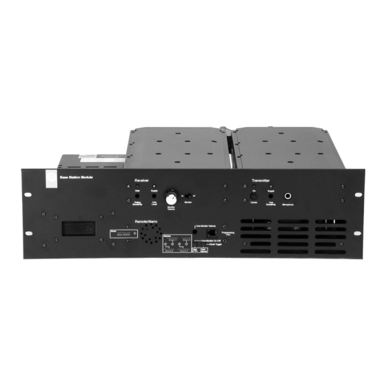
- Page 245 The T803-02 interfaces with the SL2 receiver and transmitter via the backplane PCB (X800-56-PCB3) and two small flat cable looms plugged into the D- ranges on the back. The T803 is configured using the Tait PGM800Win programming software (V4.02 and later) on a PC.
-
Page 246: Other Features
Other Features • Programmable Morse Code Encoder for automatic station identification (CWID) • User programmable Line levels • Programmable Transmit and Receive audio path delays • Programmable (on/off) notch filtering. © Copyright Tait Electronics Limited August 2004. All rights reserved. - Page 247 Mode LED The colour of the Mode LED on the front panel indicates the T803 mode of operation: • Green = Base station mode • Red = Repeater (talk through) mode © Copyright Tait Electronics Limited August 2004. All rights reserved.
- Page 248 Auxiliary 0.32s on/0.1s off alternating red and green Rack and Auxiliary 0.32s on/0.1s off/ 0.32s on/0.1s off Press the Monitor and Mode Toggle buttons together to reset all alarms. © Copyright Tait Electronics Limited August 2004. All rights reserved.
-
Page 249: Specifications
HKTA 2023 (Hong Kong): Programmable Line Output level must be set to ≤ –10dBm. For compliance with ACA TS002 (Australia): Programmable Line Output level must be set to ≤ –11dBm. © Copyright Tait Electronics Limited August 2004. All rights reserved. - Page 250 … ±24Hz typical Maximum Number of Function Tones … 2 Programmable Function Tone Duration … 20 to 100ms 1.2.6 Audio Response Frequency Response … ±1dB 300Hz to 3kHz except at notch frequency © Copyright Tait Electronics Limited August 2004. All rights reserved.
-
Page 251: Morse Code
(for test tone set at 60%) Alarm Pip Tone Frequency/Duration … 600Hz/200ms on tail of audio 1.2.8 Morse Code Sending Speed … 20 words per minute (PARIS) Maximum Code Length … 15.36 seconds © Copyright Tait Electronics Limited August 2004. All rights reserved. - Page 252 … –40dBr to –1dBr (Adjustable relative to Line-Out setting) 1.2.10 Miscellaneous Auxiliary Output Rating … open collector, 50V, 250mA (at25°C) Momentary Monitor (CTCSS Defeat) Time … off or 1 to 20 seconds © Copyright Tait Electronics Limited August 2004. All rights reserved.
-
Page 253: System Configuration
T803 Tone Remote. Refer to Section 1.3.1 for details on the product types mentioned in this chart. Part C, Section 3.10 Part B, Section Figure 1.2 T803 System Configuration © Copyright Tait Electronics Limited August 2004. All rights reserved. -
Page 254: Product Codes
General Information M8SL2-00-002-812 1.3.1 Product Codes The following table provides a brief description of the products mentioned in Figure 1.2. Consult your nearest Tait Dealer or Customer Service Organisation for more informa- tion on these products. Product Code Description T800-04-0000 T800 UHF RSSI kit. - Page 255 Phone: 0800 320 4037 Fax: 281 829-3320 Mobile: 713-703-4991 Only approved Tait Dealer or Customer Service Organisations equipped with the necessary facilities should perform any servicing. Repairs attempted with incor- rect equipment or untrained personnel may result in permanent damage. If the...
- Page 256 The T803-02 Tone Remote and Alarm Interface unit is supplied together with the follow- ing separate EMC Filter: 069-00010-31 Description Clamp-on ferrite EMC filter for 13mm diameter cable Manufacturer and part number Fair-Rite Part No. 0431 164181 © Copyright Tait Electronics Limited August 2004. All rights reserved.
- Page 257 Single turn Double turn Figure 1.3 Single and double turn of line through filter Technical Support Contact your local Tait Electronics agent or Customer Service Organisation or visit Tait Electronics Technical Support at support.taitworld.com. 1.4.4 New Zealand This product complies with the following standards: •...
- Page 258 AS/NZS 3548 Class A Radiated and conducted emissions specifications 1.4.6 Hong Kong This product complies with the Network Connection specification HKTA 2023 1.4.7 Singapore This product complies with the Type Approval specification IDA TS PSTN1 © Copyright Tait Electronics Limited August 2004. All rights reserved.
-
Page 259: Circuit Operation
The following topics are covered in this section. Section Title Page Circuit Overview Tone Detection Alarm Monitoring 2.3.1 Alarm Triggers Confirmations Clearing Alarms and Confirmations Voting Tone Operation Figure Title Page High Level Block Diagram Signal Flow © Copyright Tait Electronics Limited August 2004. All rights reserved. - Page 260 D2.2 Circuit Operation M8SL2-00-002-812 © Copyright Tait Electronics Limited August 2004. All rights reserved.
-
Page 261: Circuit Overview
• generate voting tones to Line-Out; • generate morse code to transmitter audio; • cross connect line and radio audio paths; • adjusts the Line-In and Line-Out levels; © Copyright Tait Electronics Limited August 2004. All rights reserved. - Page 262 DSP to gate audio from the receiver to Line-Out. If the line interface is 2- wire, Line-In and Line-Out are joined and the Rx audio will pass through the line inter- © Copyright Tait Electronics Limited August 2004. All rights reserved.
-
Page 263: Alarm Monitoring
Sub-rack alarms (Fwd and Rev Power, Low battery or Line fail) cannot be re-triggered until they are cleared. The 4 external closure alarms however will re-send any user programmed tone sequence if re-triggered when already latched. © Copyright Tait Electronics Limited August 2004. All rights reserved. -
Page 264: Alarm Type
If no keying from line occurs within the period programmed by the user from PGM800Win, the microprocessor latches this alarm, saves the mode status and puts the T803 into repeater mode. Note that programming zero as the line fail time disables this alarm. © Copyright Tait Electronics Limited August 2004. All rights reserved. - Page 265 It is possible to have more than one Alarm or Confirmation using the pip tone. In this situation the clearing behaviour must be carefully considered: • Line Fail Pip – Cleared by line keying-sequence only if pip tone is not ‘active’ for other Alarms and/or Confirmations. © Copyright Tait Electronics Limited August 2004. All rights reserved.
- Page 266 DSP. The DSP generates a voting tone to Line-Out. The tone fre- quency is proportional to the RSSI level. To prevent incorrect operation of the far end voting equipment, the DSP low pass filters the receiver audio transmitted to Line-Out. © Copyright Tait Electronics Limited August 2004. All rights reserved.
- Page 267 Circuit Operation D2.9 M8SL2-00-002-812 Figure 2.2 Signal Flow © Copyright Tait Electronics Limited August 2004. All rights reserved.
- Page 268 D2.10 Circuit Operation M8SL2-00-002-812 © Copyright Tait Electronics Limited August 2004. All rights reserved.
-
Page 269: Installation And Configuration
Tx Audio – Audio Level from T803 to Transmitter 3.11 3.2.4.2 Line-In Level 3.11 3.2.4.3 Rx Audio – Audio Level from Receiver to T803 3.12 3.2.4.4 Line-Out Level 3.15 Fault Finding 3.15 3.3.1 Troubleshooting 3.16 © Copyright Tait Electronics Limited August 2004. All rights reserved. - Page 270 D3.2 Installation and Configuration M8SL2-00-002-812 Figure Title Page X800-56-PCB3 backplane connectors, links and switches T803 setup Rack and test equipment setup Cycle of switching between the modes © Copyright Tait Electronics Limited August 2004. All rights reserved.
-
Page 271: Backplane Configuration
T854. See Section 3.10 in Part LN10 Link pins 2 – 3 REV power alarm signal to T803. LN11 Fitted RX CTCSS disable See Section 6.2 in Part G © Copyright Tait Electronics Limited August 2004. All rights reserved. - Page 272 Set switch 6 to ON Rx-Gate to T803 Note: For correct power alarm operation these links should be correctly set before power-up. Figure 3.1 X800-56-PCB3 backplane connectors, links and switches © Copyright Tait Electronics Limited August 2004. All rights reserved.
- Page 273 Maximum applied voltage = 50V AUX2 Maximum sink current = 250mA T803 Auxiliary Output 3. TONE REMOTE Maximum applied voltage = 50V AUX3 Maximum sink current = 250mA — — Ground © Copyright Tait Electronics Limited August 2004. All rights reserved.
-
Page 274: Line Interface
LineOut- The T803 accommodates an input signal range of 28dB. Normally this is sufficient, how- ever by shorting JP200 (found on the T803 PCB) an extra 15dB gain is added. © Copyright Tait Electronics Limited August 2004. All rights reserved. - Page 275 T803 levels can be properly calculated and programmed. Setting up receiver and transmitter levels can only be done using T803 test modes and/ or measurement. These levels are not programmable. © Copyright Tait Electronics Limited August 2004. All rights reserved.
- Page 276 T803’s built in speaker without broadcasting speech to air. The service personnel can talk back to the dispatcher using the T803 test microphone (the PTT must be pressed to gate microphone speech). © Copyright Tait Electronics Limited August 2004. All rights reserved.
-
Page 277: Test Modes
1. Line-Out Configuration Mode is only available in T803 firmware version 2.07 or later. For firmware versions prior to 2.07, a simultaneous button press while in Line-In Con- figuration Mode will exit Test Mode . © Copyright Tait Electronics Limited August 2004. All rights reserved. - Page 278 • Rx Audio – Audio level from receiver to T803 (unbalanced) • Line-Out level The only consideration of order is that the Tx Audio level needs to be configured before the Line-In level can be done. © Copyright Tait Electronics Limited August 2004. All rights reserved.
- Page 279 Press the PTT on the dispatch console again, but this time use speech instead of the test tone. Ensure the LEDs on the T803 remain constant on green during speech transmission. If not see Section 3.3.1 (point 7) on how to troubleshoot for Talkoff. © Copyright Tait Electronics Limited August 2004. All rights reserved.
- Page 280 See Section 3.5 in Part B. The T803 does however apply a 160Hz to 3kHz high pass filter resulting in an overall audio response for this path very similar to the default high pass filtered receiver balanced Line output. See the table below. © Copyright Tait Electronics Limited August 2004. All rights reserved.
- Page 281 LN8, with the links (jumpers) in place as directed in Section 3.1.1. Use a high impedance meter such as an oscilloscope for the measurement. 1. A 1020Hz tone is used (rather than 1kHz) because some Test Sets can produce unstable deviation readings © Copyright Tait Electronics Limited August 2004. All rights reserved.
- Page 282 ‘Line-Out Level’ as set in PGM800Win. 1. The Mode Toggle button may be disabled from PGM800Win 2. A 1020Hz tone is used (rather than 1kHz) because some Test Sets can produce unstable deviation readings © Copyright Tait Electronics Limited August 2004. All rights reserved.
-
Page 283: Fault Finding
Connect the T803 to its companion dispatch console via the leased line. Check that speech sent from the console can be heard on the T803 speaker (un-mute speaker if required). © Copyright Tait Electronics Limited August 2004. All rights reserved. - Page 284 PGM800Win with full T803 support. Loop-Line functionality (also known as Loopback) Loopback can be enabled in PGM800Win. It is then activated by sending the T803 the programmed function tones. © Copyright Tait Electronics Limited August 2004. All rights reserved.
- Page 285 Sensitivity control on the front panel of the receiver, so that the receiver mute opens at a higher SINAD level (12dB or preferably greater). This has the effect of reducing the noise on the line input of the T803 in 2-wire mode. © Copyright Tait Electronics Limited August 2004. All rights reserved.
- Page 286 2-wire/4-wire hybrid fitted across the line may be required. This solution has been veri- fied and documentation is available detailing how to install the TA1086-01. Contact your your nearest Tait Dealer or Customer Service Organisation for more information. © Copyright Tait Electronics Limited August 2004. All rights reserved.
- Page 287 This section provides the following information on the T803. • parts list • grid reference index • PCB layouts • circuit diagrams. Section Title Page Introduction 4.1.3 T803 Main and Front Panel PCBs 220-01581-01 4.2.1 © Copyright Tait Electronics Limited August 2004. All rights reserved.
- Page 288 D4.1.2 T803 PCB Information M8SL2-00-002-812 © Copyright Tait Electronics Limited August 2004. All rights reserved.
-
Page 289: Pcb Identification
Internal Part Number - order the component by this number The mechanical and miscellaneous section lists the variant and common parts in IPN order. © Copyright Tait Electronics Limited August 2004. All rights reserved. - Page 290 (e.g. 1R3). C371 DISCRIMINATOR %R338 R339 C369 100K 100P these grid references show where the circuit is continued C301 IF-SIG R303 L310 © Copyright Tait Electronics Limited August 2004. All rights reserved.
- Page 291 Overview and Front Panel Circuit Diagram 4.2.11 Interface Circuit Diagram 4.2.12 Control and Processing Circuit Diagram 4.2.13 P100 PI Filters Circuit Diagram 4.2.14 SK100 PI Filters Circuit Diagram 4.2.15 SK102 PI Filters Circuit Diagram 4.2.16 © Copyright Tait Electronics Limited August 2004. All rights reserved.
- Page 292 D4.2.2 T803 PCB Information M8SL2-00-002-812 © Copyright Tait Electronics Limited August 2004. All rights reserved.
- Page 293 CAP CER 0805 1N 10% X7R 50V C600 015-24100-08 CAP CER 0805 1N 10% X7R 50V C409 015-24100-08 CAP CER 0805 1N 10% X7R 50V C601 015-22270-01 CAP CER 0805 27P 5% NPO 50V © Copyright Tait Electronics Limited August 2004. All rights reserved.
- Page 294 IND 0805 120E@100M .2 EMI SUPR R320 036-15100-10 RES M/F SMD 0805 10K 1% L511 057-10120-03 IND 0805 120E@100M .2 EMI SUPR R321 036-14470-10 RES M/F SMD 0805 4K7 1% © Copyright Tait Electronics Limited August 2004. All rights reserved.
- Page 295 CONN SMD 16W 2R SKT M/MATCH 240-04021-60 SKT 6W MODR PH VRT T-ENT T200 054-00010-16 XFMR LINE 600 OHM 1:1 P1200 T201 054-00010-16 XFMR LINE 600 OHM 1:1 P1200 XL300 274-00010-59 XTAL 18.432MHZ HC49/U © Copyright Tait Electronics Limited August 2004. All rights reserved.
- Page 296 SCRW M4*10MM CSK POZI S/T BZ 349-00020-09 SCRW 4-40*3/8" T/T P/P BLK 349-00020-08 SCRW 4-40*3/8" T/T CSK POZI BZ 349-00020-55 SCRW M3*8MM T/T P/P BZ 369-01039-00 ADH RING 40MM T/ORCA SPKR © Copyright Tait Electronics Limited August 2004. All rights reserved.
- Page 297 2-M7 C438 1:D5 4-J0 C613 1:L4 6-G3 JP301 1:J15 3-E5 C300 1:L15 3-A9 C439 1:D4 4-J0 JP302 1:J15 3-F5 C301 1:M15 3-B9 C440 1:D8 4-J9 2:T9 1-T2 JP303 1:J15 3-E4 © Copyright Tait Electronics Limited August 2004. All rights reserved.
- Page 298 R272 1:K5 2-G0 TP216 1:E13 2-N9 1:R7 1-T3 R273 1:G12 2-S7 TP300 1:J12 3-C5 1:S9 1-S2 R274 1:G12 2-S5 TP301 1:J12 3-C5 1:S9 1-T2 R275 1:G12 2-S3 TP302 1:H13 3-C4 © Copyright Tait Electronics Limited August 2004. All rights reserved.
- Page 299 C527 FID1 IPN: ISS: DATE: TAIT ELECTRONICS 220-01581-04 1.TA 1 Mar 2002 T803 / T805 PCB LAYOUT - TOP SIDE Scale:1.5:1 Rotation: degrees T803 PCB Layout – Top Side 220-01581-04 © Copyright Tait Electronics Limited August 2004. All rights reserved.
- Page 300 BSLOT BHOLE IPN: ISS: DATE: TAIT ELECTRONICS 220-01581-04 4.BA 1 Mar 2002 T803 / T805 PCB LAYOUT - BOTTOM SIDE Scale:1.5:1 Rotation: degrees T803 PCB Layout – Bottom Side 220-01581-04 © Copyright Tait Electronics Limited August 2004. All rights reserved.
- Page 301 CRAIG M. PROJECT: DESIGNER: FILE NAME: FILE DATE: NO.SHEETS: REV/ISS AMENDMENTS DRAWN CHKD D.O. APVD DATE T803 TONY S 158104a 1-Mar-02 Sheet 1 – T803 Overview and Front Panel 220-01581-04 © Copyright Tait Electronics Limited August 2004. All rights reserved.
- Page 302 IPN 220-01581-04 D4.2.12 T803 PCB Information M8SL2-00-002-812 Sheet 2 – T803 Interface 220-01581-04 © Copyright Tait Electronics Limited August 2004. All rights reserved.
- Page 303 ORIGINAL CRAIG M. PROJECT: DESIGNER: FILE NAME: FILE DATE: NO.SHEETS: REV/ISS AMENDMENTS DRAWN CHKD D.O. APVD DATE T803 TONY S 158104a 1-Mar-02 Sheet 3 – T803 Control and Processing 220-01581-04 © Copyright Tait Electronics Limited August 2004. All rights reserved.
- Page 304 ORIGINAL CRAIG M. PROJECT: DESIGNER: FILE NAME: FILE DATE: NO.SHEETS: REV/ISS AMENDMENTS DRAWN CHKD D.O. APVD DATE T803 TONY S 158104a 1-Mar-02 Sheet 4 – T803 P100 PI filters 220-01581-04 © Copyright Tait Electronics Limited August 2004. All rights reserved.
- Page 305 ORIGINAL CRAIG M. PROJECT: DESIGNER: FILE NAME: FILE DATE: NO.SHEETS: REV/ISS AMENDMENTS DRAWN CHKD D.O. APVD DATE T803 TONY S 158104a 1-Mar-02 Sheet 5 – T803 SK101 PI Filters 220-01581-04 © Copyright Tait Electronics Limited August 2004. All rights reserved.
- Page 306 ORIGINAL CRAIG M. PROJECT: DESIGNER: FILE NAME: FILE DATE: NO.SHEETS: REV/ISS AMENDMENTS DRAWN CHKD D.O. APVD DATE T803 TONY S 158104a 1-Mar-02 Sheet 6 – T803 SK102 PI Filters 220-01581-04 © Copyright Tait Electronics Limited August 2004. All rights reserved.
- Page 307 This part of the manual provides the parts list, PCB layouts and circuit diagram for the T850 VCO PCB. There is a detailed table of contents at the start of Section 2. Section Title Page Introduction T850 VCO PCB 220-01145-07 © Copyright Tait Electronics Limited August 2004. All rights reserved.
- Page 308 M8SL2-00-002-812 © Copyright Tait Electronics Limited August 2004. All rights reserved.
-
Page 309: Pcb Identification
Internal Part Number - order the component by this number The mechanical and miscellaneous section lists the variant and common parts in IPN order. © Copyright Tait Electronics Limited August 2004. All rights reserved. - Page 310 A variant component is one that has the same circuit reference but different value or specification in different product types. Variant components have a character prefix, such as “&”, “=” or “#”, before the circuit reference (e.g. &R100). © Copyright Tait Electronics Limited August 2004. All rights reserved.
- Page 311 T850 VCO PCB Information E2.1 M8SL2-00-002-812 T850 VCO PCB This section contains the following information. Section Page 220-01145-07 Parts List PCB Layout – Bottom Side PCB Layout – Top Side Circuit Diagram © Copyright Tait Electronics Limited August 2004. All rights reserved.
- Page 312 E2.2 T850 VCO PCB Information M8SL2-00-002-812 © Copyright Tait Electronics Limited August 2004. All rights reserved.
- Page 313 057-00047-10 Ind Fxd 47nh +-5% 1206 056-10015-03 Ind SMD 0805cs 15nh 20% 056-10015-03 Ind SMD 0805cs 15nh 20% 056-10015-03 Ind SMD 0805cs 15nh 20% 056-10015-03 Ind SMD 0805cs 15nh 20% © Copyright Tait Electronics Limited August 2004. All rights reserved.
- Page 314 IPN 220-01145-07 E2.4 T850 VCO PCB Information M8SL2-00-002-812 T850 VCO PCB (IPN 220-01145-07) – Top Side © Copyright Tait Electronics Limited August 2004. All rights reserved.
- Page 315 IPN 220-01145-07 T850 VCO PCB Information E2.5 M8SL2-00-002-812 T850 VCO PCB (IPN 220-01145-07) – Bottom Side © Copyright Tait Electronics Limited August 2004. All rights reserved.
- Page 316 E2.6 T850 VCO PCB Information M8SL2-00-002-812 © Copyright Tait Electronics Limited August 2004. All rights reserved.
- Page 317 SMD PARTS ADDED BENC 07-10-99 220-01145-07 2.SC. CYCLIC KEYING MODIFICATION BENC PROJECT: DESIGNER: FILE NAME: FILE DATE: NO.SHEETS: REV/ISS AMENDMENTS DRAWN CHKD D.O. APVD DATE T850 SSAHI 1145_07b 10-Jun-03 T850 VCO 220-01145-07 © Copyright Tait Electronics Limited August 2004. All rights reserved.
- Page 318 IPN 220-01145-07 E2.8 T850 VCO PCB Information M8SL2-00-002-812 © Copyright Tait Electronics Limited August 2004. All rights reserved.
- Page 319 This part of the manual provides information on the power supply, and is divided into six sections as listed below.. Section Title General Information Power Supply Description Installation Guidelines Functional Testing Troubleshooting Service Information © Copyright Tait Electronics Limited August 2004. All rights reserved.
- Page 320 M8SL2-00-002-812 © Copyright Tait Electronics Limited August 2004. All rights reserved.
- Page 321 Introduction The T800-23-0011 is a switching power supply designed to meet the requirements of the T800 SL2 25W Continuous Basestation. It is capable of suppling 13.8V at up to 14.5A (see derating information in Section 1.2.4). The unit provides power to the T800 SL2 Bas- estation modules via a cable assembly (with a 12A fuse) which connects between the DC output connector on the back of the unit, and the backplane PCB (X800-56-PCB3).
-
Page 322: Specifications
AC Input Current … 2.8A maximum (115V at full load) Maximum Inrush Current … 40A maximum (230V at full load) Connection to mains supply … IEC plug on rear panel © Copyright Tait Electronics Limited August 2004. All rights reserved. - Page 323 … 15.2 to 21.8A Type: Constant current limiting Reset: Auto recovery Output Connector … Molex 6-way receptacle Note: Refer to Figure 3.1 in Section 3.2 for the output connector pinouts. © Copyright Tait Electronics Limited August 2004. All rights reserved.
-
Page 324: Emc Conformity
© Copyright Tait Electronics Limited August 2004. All rights reserved. -
Page 325: Safety Approvals
Warning: Safety approval will become void if T800-23-0011 components are replaced with non-equivalent rated or non-certified/approved components. Contact Tait Electronics Technical Support before replacing components of the T800-23-0011. See Section 6 for important servicing information. © Copyright Tait Electronics Limited August 2004. All rights reserved. - Page 326 F1.6 General Information M8SL2-00-002-812 © Copyright Tait Electronics Limited August 2004. All rights reserved.
-
Page 327: Power Supply Description
(DC Output filter) Chassis grounding point using Earth Tag Molex Socket IEC Plug (DC Output) (Mains Input) Figure 2.1 T800-23-0011 internal view. See the Parts List in Section 6.2.2 for more detail. © Copyright Tait Electronics Limited August 2004. All rights reserved. - Page 328 SL2 backplane and the SL2 front panel. The external cable connection between the T800-23-0011 and the SL2 backplane completes this path. For the wiring diagram, refer to Section 6.2.1. © Copyright Tait Electronics Limited August 2004. All rights reserved.
-
Page 329: Connector Pinouts
IEC Plug (Mains Input) Molex Socket (DC Output) Neutral Live +13.8V Ground Ground Programming port Earth (from front panel) Speaker (to front panel) Figure 3.1 Connector Pinouts on the T800-23-0011 rear panel. © Copyright Tait Electronics Limited August 2004. All rights reserved. -
Page 330: Equipment Cooling
It is estimated that the average life expectancy of this unit will double with every 10°C drop in ambient temperature. It is therefore recommended to: • Keep the ambient temperature low. • Ensure that airflow is not restricted. © Copyright Tait Electronics Limited August 2004. All rights reserved. -
Page 331: Functional Testing
• Switch on the mains supply and slowly decrease the load resistance, thereby increasing the current until voltage foldback occurs. The current should not rise above the Current Overload Limit (refer to Section 1.2.4), but voltage should drop away. © Copyright Tait Electronics Limited August 2004. All rights reserved. -
Page 332: Output Noise
• Connect the oscilloscope across the output. • Vary the mains voltage and DC load over the full specified range (refer to Section 1.2). • Check on the oscilloscope that no oscillations occur. © Copyright Tait Electronics Limited August 2004. All rights reserved. -
Page 333: Troubleshooting
Equipment cooling is inef- Refer to Section 3.3 for ficient due to incorrect installation guidelines installation of the T800-23-0011 The T800-23-0011 internal Replace module or return fan has failed faulty module for servic- © Copyright Tait Electronics Limited August 2004. All rights reserved. - Page 334 F5.2 Troubleshooting M8SL2-00-002-812 © Copyright Tait Electronics Limited August 2004. All rights reserved.
-
Page 335: Service Information
Although this is a lightweight unit, it contains a number of quite heavy and fragile indi- vidual components which are mounted directly on the PCB. Severe mechanical shock may damage the PCB (e.g. solder joints, copper tracks) and/or components (e.g. fragile ferrite magnetic materials). © Copyright Tait Electronics Limited August 2004. All rights reserved. -
Page 336: Wiring Diagram
Brown Black IEC Mains Connector Green&Yellow Ground Black Chassis Ground Blue Neutral +13.8V Brown Live Ferrite Sleeve Ferrite Beads Molex Connector External view PSU Module Figure 6.1 T800-23-0011 Wiring Diagram © Copyright Tait Electronics Limited August 2004. All rights reserved. -
Page 337: Assembly Drawing
Service Information F6.3 M8SL2-00-002-812 6.2.2 Assembly Drawing Figure 6.2 below shows an exploded view of the T800-23-0011. Figure 6.2 Mechanical assembly of the T800-23-0011. © Copyright Tait Electronics Limited August 2004. All rights reserved. - Page 338 F6.4 Service Information M8SL2-00-002-812 © Copyright Tait Electronics Limited August 2004. All rights reserved.
- Page 339 Direct input to Buffer option 2.10 Line Input Control Replacement Talk Through Repeater Line Controlled Base without Talk Through 4.11 General 4.12 Transmitter Tail Timer DC Line Keying X800-56-PCB3 PCB Information 6.1.1 © Copyright Tait Electronics Limited August 2004. All rights reserved.
- Page 340 Remote Line Controlled Base Station 4-Wire to 2-Wire Converter Receiver Disable Time vs Tail Time DC Loop Keying With Common Earth Isolated Constant Current Loop Current Detector Isolated Loop Current Switch Typical System © Copyright Tait Electronics Limited August 2004. All rights reserved.
-
Page 341: Power Supply
The circuit breaker will disconnect the mains to the entire rack. If only one channel needs to be mains-isolated and the Tait power supply module is T800-23-0011, then it is acceptable practice to pull the IEC connector directly out of the power supply module. - Page 342 It also provides overvoltage protection from voltage transients caused by lightning strikes. Note: A fuse must be fitted in the power supply line for the diode to provide effec- tive protection. © Copyright Tait Electronics Limited August 2004. All rights reserved.
- Page 343 Open drain type; AUX-OUT 1 capable of sinking CH_SLCT 6 2.25mA via 2k2Ω; AUX-OUT 2 max. = 5V Figure 1.2 T855 D-Range 2 Wiring – Rear View (standard T800-03-0000 kit) © Copyright Tait Electronics Limited August 2004. All rights reserved.
- Page 344 Note: Figure 1.4 above shows the standard pin allocations for the T800-03-0000 auxiliary D-range kit. A T800-03 auxiliary D-range kit is also available for special applications requiring custom internal wiring. © Copyright Tait Electronics Limited August 2004. All rights reserved.
- Page 345 If access to the rear of the rack frame is restricted, the cable should be long enough to allow the slimline assembly to be fully withdrawn from the cabinet. Make sure that any N-type plugs connected to Tait equipment are assembled according to the manufacturer’s instructions. It is particularly important that the centre pin in the plug is positioned correctly: •...
- Page 346 G1.6 M8SL2-00-002-812 © Copyright Tait Electronics Limited August 2004. All rights reserved.
- Page 347 T800 SL2 G1.7 M8SL2-00-002-812 Figure 1.6 T800 SL2 Assembly – with T803 fitted © Copyright Tait Electronics Limited August 2004. All rights reserved.
- Page 348 G1.8 T800 SL2 M8SL2-00-002-812 Figure 1.7 T800 SL2 Assembly – without T803 fitted © Copyright Tait Electronics Limited August 2004. All rights reserved.
- Page 349 T800 SL2 G1.9 M8SL2-00-002-812 Transmitter Receiver Power Supply Power Rating Label Front Panel Backplane PCB Tone Remote Figure 1.8 T800 SL2 Assembly – with T803 fitted (rear view) © Copyright Tait Electronics Limited August 2004. All rights reserved.
- Page 350 G1.10 T800 SL2 M8SL2-00-002-812 © Copyright Tait Electronics Limited August 2004. All rights reserved.
-
Page 351: Audio Processor
The letters in this column refer to the letters printed on the PCB beside each pair of pins. Note that the link names and pin numbers are different to earlier products. The lettering A to N is however the same. b. Factory Setting © Copyright Tait Electronics Limited August 2004. All rights reserved. - Page 352 Line transformer. %T210A and %T210B use a standard footprint which allows the use of other similar transformers with special characteristics, such as the ETAL P3181 ultra-low distortion V.90 SMD. © Copyright Tait Electronics Limited August 2004. All rights reserved.
- Page 353 Common Earth systems. If full isolated DC loop keying is required, then the T4030 must still be used. The T4030 must also be used if the Transmitter is to be used as half of a 2-wire to 4-wire hybrid. © Copyright Tait Electronics Limited August 2004. All rights reserved.
- Page 354 R240 and R243 have replaced SL203 and SL204, originally on the T856 underside. These connect the opto key to D-range 1 pins 11 and 12, and when removed free the D-range pins for alternative use. © Copyright Tait Electronics Limited August 2004. All rights reserved.
-
Page 355: Relay Driver
Transmit Key Time SL501 standard 30ms (approx.) not linked short* <5ms linked *In this configuration the standby spurious emissions should be <–65dBm. © Copyright Tait Electronics Limited August 2004. All rights reserved. - Page 356 2.10 Line Input Control Replacement The Line Input control can be replaced with fixed resistors if required. Enabled Disabled %R222 Not fitted %R234 Not fitted %RV210 Not fitted 10K Log © Copyright Tait Electronics Limited August 2004. All rights reserved.
-
Page 357: Talk Through Repeater
'N' Socket Typical line level -15dBm Line Out Line In Receiver Transmitter Tx Key Out Tx Key In Monitor Mic. Monitor Local Speaker Microphone 13.8V Supply Figure 3.1 Talk Through Repeater © Copyright Tait Electronics Limited August 2004. All rights reserved. - Page 358 G3.2 Talk Through Repeater M8SL2-00-002-812 © Copyright Tait Electronics Limited August 2004. All rights reserved.
- Page 359 Relay Rx Disable Figure 4.2 Basic Configuration Antenna RF Out RF In Coax Relay Hybrid Rx AF Tx AF Microphone Remote Speaker Control Figure 4.3 Remote Line Controlled Base Station © Copyright Tait Electronics Limited August 2004. All rights reserved.
- Page 360 Q250 (D-range 2 pin 9). © Copyright Tait Electronics Limited August 2004. All rights reserved.
- Page 361 (refer to Figure 5.7, Figure 5.8 and Figure 5.9). Figure 5.7 Isolated Constant Current Loop Current Detector (Opto-key input on T854) © Copyright Tait Electronics Limited August 2004. All rights reserved.
- Page 362 DC Line Keying M8SL2-00-002-812 Figure 5.8 Isolated Loop Current Switch Long Line Unit 1 Unit 2 Optional bridge to protect against Isolated polarity reversals Supply (T223 only). Figure 5.9 Typical System © Copyright Tait Electronics Limited August 2004. All rights reserved.
- Page 363 This section contains the following information. Section Page 220-01702-02 Backplane Links and Switches 6.2.3 Parts List 6.2.5 PCB Layout – Top Side 6.2.7 PCB Layout – Bottom Side 6.2.8 Circuit Diagram 6.2.9 © Copyright Tait Electronics Limited August 2004. All rights reserved.
- Page 364 This part of the manual provides the parts list, PCB layouts and circuit diagram for the X800-56-PCB3 backplane PCB. There is a detailed table of contents at the start of Section 2. Section Title Page Introduction 6.1.1 X800-56-PCB3 backplane PCB 220-01702-02 6.2.1 © Copyright Tait Electronics Limited August 2004. All rights reserved.
- Page 365 G6.1.2 X800-56-PCB3 PCB Information M8SL2-00-002-812 © Copyright Tait Electronics Limited August 2004. All rights reserved.
- Page 366 Internal Part Number - order the component by this number The mechanical and miscellaneous section lists the variant and common parts in IPN order. © Copyright Tait Electronics Limited August 2004. All rights reserved.
- Page 367 (e.g. 1R3). C371 DISCRIMINATOR %R338 R339 C369 100K 100P these grid references show where the circuit is continued C301 IF-SIG R303 L310 © Copyright Tait Electronics Limited August 2004. All rights reserved.
- Page 368 G6.2.2 X800-56-PCB3 PCB Information M8SL2-00-002-812 © Copyright Tait Electronics Limited August 2004. All rights reserved.
- Page 369 Connects RX CTCSS disable from the T803 to the LN11 receiver. Connects Tx-Relay-Driver output from the transmitter Recommended setting to prevent the receiver LN12 to RX-Inhibit on the receiver. mute from inadvertently opening. Table 6.1 X800-56-PCB3 links © Copyright Tait Electronics Limited August 2004. All rights reserved.
- Page 370 ( SK13 pin9 ) T803 CTCSS audio not available at SW3-7 When ON connects T803 CTCSS audio to the transmitter. time of publication. SW3-8 Not used. Figure 6.10 X800-56-PCB3 switches © Copyright Tait Electronics Limited August 2004. All rights reserved.
- Page 371 240-00010-79 SKT 10WAY 2X5 AMP MICRO MATCH TOP ENTRY 230-00010-19 DIP-8 SW X 8 SPST DIP 230-00010-19 DIP-8 SW X 8 SPST DIP 230-00010-19 DIP-8 SW X 8 SPST DIP © Copyright Tait Electronics Limited August 2004. All rights reserved.
- Page 372 IPN 220-01702-02 G6.2.6 X800-56-PCB3 PCB Information M8SL2-00-002-812 © Copyright Tait Electronics Limited August 2004. All rights reserved.
- Page 373 IPN 220-01702-02 X800-56-PCB3 PCB Information G6.2.7 M8SL2-00-002-812 X800-56-PCB3 PCB (IPN 220-01702-02) – Top Side 220-01702-02 © Copyright Tait Electronics Limited August 2004. All rights reserved.
- Page 374 IPN 220-01702-02 G6.2.8 X800-56-PCB3 PCB Information M8SL2-00-002-812 X800-56-PCB3 PCB (IPN 220-01702-02) – Bottom Side 220-01702-02 © Copyright Tait Electronics Limited August 2004. All rights reserved.
- Page 375 IPN 220-01702-02 X800-56-PCB3 PCB Information G6.2.9 M8SL2-00-002-812 X800-56-PCB3 circuit diagram 220-01702-02 © Copyright Tait Electronics Limited August 2004. All rights reserved.
- Page 376 IPN 220-01702-02 G6.2.10 X800-56-PCB3 PCB Information M8SL2-00-002-812 © Copyright Tait Electronics Limited August 2004. All rights reserved.
- Page 377 This part of the manual features a brief description of the major ancillaries that may be used with T800 SL2 equipment. For a comprehensive list of available ancillary equip- ment, please contact your nearest Tait Dealer or Customer Service Organisation. Section...
- Page 378 M8SL2-00-002-812 © Copyright Tait Electronics Limited August 2004. All rights reserved.
- Page 379 PCB), or into SK805 in the microcontroller compartment via the supplied ribbon cable loom, and is then connected to the PC with a T800-01-0002 programming cable. Refer to the T800 Ancillary Equipment Service Manual for more information. © Copyright Tait Electronics Limited August 2004. All rights reserved.
- Page 380 Typical uses of the T800-03-0000 are in paging applica- tions and where external channel control is required. Refer to for the Figure 1.4 Part G T800-03-0000 pin connections. © Copyright Tait Electronics Limited August 2004. All rights reserved.
- Page 381 300mm cord terminated in a ¼” stereo plug for use with the T854. T800-80-0001 T803 Microphone Ω A 600 microphone complete with 300mm cord terminated with a RJ11connector for use with the T803. © Copyright Tait Electronics Limited August 2004. All rights reserved.
- Page 382 (e.g. tone or speech). The T800-32-0010 is adapted for use with an external reference oscillator for simulcast transmission. The T800-32-0000 and T800-32-0010 are not designed for use with 66 to 88MHz equipment. © Copyright Tait Electronics Limited August 2004. All rights reserved.
-
Page 383: External Frequency Reference
T801-10 is a high quality ovenised crystal oscillator (OCXO). Three outputs are provided on the rear panel, which allows up to three T800 SL2 transmitters to be referenced to the source oscillator. Refer to M801-10. © Copyright Tait Electronics Limited August 2004. All rights reserved.
Need help?
Do you have a question about the T800 SL2 25W and is the answer not in the manual?
Questions and answers