
Related Manuals for iWave iW-RainboW-G25S


Summary of Contents for iWave iW-RainboW-G25S
- Page 1 Snapdragon 820 SBC Hardware User Guide iW-RainboW-G25S Snapdragon 820 Single Board Computer Hardware User Guide REL1.0 iWave Systems Technologies Pvt. Ltd. Page 1 of 33...
- Page 2 If you are not the intended recipient (or authorized to receive for the recipient), you are hereby notified that any disclosure, copying distribution or use of any of the information contained within this document is STRICTLY PROHIBITED. Thank you. “iWave Systems Tech. Pvt. Ltd.” REL1.0 iWave Systems Technologies Pvt.
- Page 3 (including liability to any person by reason of negligence) will be accepted by iWave Systems, its subsidiaries or employees for any direct or indirect loss or damage caused by omissions from or inaccuracies in this document.
-
Page 4: Table Of Contents
I/O Connectors ............................24 2.10.1 30Pin I/O Connector ..........................24 2.10.2 6Pin Connector............................26 TECHNICAL SPECIFICATION ..........................27 Electrical Characteristics ..........................27 3.1.1 Power Jack ............................. 27 3.1.2 Battery Connector ..........................28 REL1.0 iWave Systems Technologies Pvt. Ltd. Page 4 of 33... - Page 5 3.2.1 Environmental Specification ........................30 3.2.2 RoHS Compliance ........................... 30 3.2.3 Electrostatic Discharge ........................... 30 Mechanical Characteristics ........................31 3.3.1 Snapdragon 820 SBC Mechanical Dimensions ..................31 ORDERING INFORMATION ..........................32 REL1.0 iWave Systems Technologies Pvt. Ltd. Page 5 of 33...
- Page 6 Table 8: Power Jack ..............................27 Table 9: Battery Connector Pin Out ........................... 28 Table 10: Power Consumption ..........................29 Table 11: Environmental Specification........................30 Table 12: Orderable Product Part Numbers ....................... 32 REL1.0 iWave Systems Technologies Pvt. Ltd. Page 6 of 33...
-
Page 7: Introduction
This document is the Hardware User Guide for the Snapdragon 820 SBC based on the Qualcomm APQ8096 Application processor (without Modem). This board is fully supported by iWave Systems Technologies Pvt. Ltd. This Guide provides detailed information on the overall design and usage of the Snapdragon 820 SBC from a Hardware Systems perspective. - Page 8 Synchronous Dynamic Random Access Memory SPMI Serial power management interface To Be Defined UART Universal Asynchronous Receiver/Transmitter Universal Serial Bus USB OTG USB On The Go Voltage Wi-Fi Wireless Fidelity REL1.0 iWave Systems Technologies Pvt. Ltd. Page 8 of 33...
-
Page 9: Terminlogy Description
Note: Signal Type does not include internal pull-ups or pull-downs implemented by the chip vendors and only includes the pull-ups or pull-downs implemented On-SBC. References • APQ8096 Hardware User Manuals REL1.0 iWave Systems Technologies Pvt. Ltd. Page 9 of 33... -
Page 10: Important Note
If CPU pin doesn’t have multiplexing option, then the signal name is mentioned as, “Function name” Example: SPMI_CLK In this signal, functionality which we are using SPMI_CLK Note: The above naming is not applicable for other signals which are not connected to CPU. REL1.0 iWave Systems Technologies Pvt. Ltd. Page 10 of 33... -
Page 11: Architecture And Design
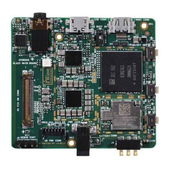
2. ARCHITECTURE AND DESIGN This section provides detailed information about the Snapdragon 820 SBC features and Hardware architecture with high level block diagram. Snapdragon 820 SBC Block Diagram iW-RainboW-G25S - Snapdragon 820 SBC Block Diagram Snapdragon 820 (APQ8096) Power Jack LPDDR4 (64bit) PMIC &... -
Page 12: Snapdragon 820 Sbc Features
USB3.0 OTG Port through USB Type-C Connector (Optional) Serial Interface Features • Debug UART through 3Pin Header On Board Switches • ON/OFF Switch • VOL+ Switch • RST/VOL- Switch • Forced USB Boot selection Switch REL1.0 iWave Systems Technologies Pvt. Ltd. Page 12 of 33... - Page 13 6pin Connector ➢ Power Out : 4.2V,2A ➢ Digital MIC Input General Specification • Power Supply : 4.2V,2A • Power Jack & Battery Connector • Form Factor : 56mm x 50mm REL1.0 iWave Systems Technologies Pvt. Ltd. Page 13 of 33...
-
Page 14: Qualcomm Apq8096 Cpu
Output power management, battery monitoring and charging. The PMI8996 mixed-signal BiCMOS device is available in the 210-pin wafer-level nanoscale package (210 WLNSP) that includes ground pins for improved electrical ground, mechanical stability, and thermal conductivity. REL1.0 iWave Systems Technologies Pvt. Ltd. Page 14 of 33... -
Page 15: Memory
SD card connector (J11) is directly connected to the SDC2 controller of the APQ8096 CPU. The main power to Micro SD Card Connector is 2.95 Voltage. Micro SD Connector is physically located on bottom side of the Snapdragon 820 SBC as shown below. Figure 2: Micro SD Connector REL1.0 iWave Systems Technologies Pvt. Ltd. Page 15 of 33... -
Page 16: Audio/Video Feature
Termination HPH_L HPH_L O, Analog Headphone Output Left. HPH_R HPH_R O, Analog Headphone Output Right. HSDET_L HSDET_L I, Analog Headphone Detection. AMIC I, Analog Microphone Input Signal. HPH_REF Power Ground. REL1.0 iWave Systems Technologies Pvt. Ltd. Page 16 of 33... -
Page 17: Hdmi Port
4k × 2k at 60 fps + 4k × 2k at 30 fps HDMI • Up to 8-channel audio for 7.1 surround sound • Dolby Digital Plus, Dolby True-HD, and DTS-HD Master Figure 4: Micro HDMI Connector REL1.0 iWave Systems Technologies Pvt. Ltd. Page 17 of 33... -
Page 18: Communication Features
MHF-4 Micro RF Coax connectors are used for interfacing the RF antenna as shown below. Receptacle: 20449-001E from IPEX Example Mating Antenna Cable: FXP830.24.0100B from Taoglas Figure 5: WLAN/BT Antenna Connector REL1.0 iWave Systems Technologies Pvt. Ltd. Page 18 of 33... -
Page 19: Gps/Gnss
GPS antenna as shown in below figure. Also connector details mentioned below. Receptacle: 20449-001E from IPEX Example Mating Antenna Cable: FXP830.24.0100B from Taoglas Figure 6: GPS Antenna Connector REL1.0 iWave Systems Technologies Pvt. Ltd. Page 19 of 33... -
Page 20: Usb 2.0 Otg Port
Snapdragon 820 SBC supports reversible cable insertion functionality for USB Type C connector a per Type C specification. The USB Type-C connector (J10) is optional feature and default not populated. Note: To add support of this optional feature in Snapdragon 820 SBC, please contact iWave Systems. REL1.0 iWave Systems Technologies Pvt. -
Page 21: Serial Interface Features
Table 4: Debug UART Header Pin Out Signal Type/ Pin Name Signal Name Description Termination BLSP8_UART_TX O, 3.3V CMOS UART Transmit signal. BLSP8_UART_RX I, 3.3V CMOS UART Receive Signal. 10K PD Power Ground REL1.0 iWave Systems Technologies Pvt. Ltd. Page 21 of 33... -
Page 22: On Board Switches
The Snapdragon 820 SBC supports Volume+ Push button switch (SW3) to increase the volume of audio out. VOL+ Push button switch (SW3) is physically located at the top of the board as shown below. Figure 10: Volume + Switch REL1.0 iWave Systems Technologies Pvt. Ltd. Page 22 of 33... -
Page 23: Rst/Vol- Switch
This mode can be used for programming the boot media and debug the CPU through USB Micro B connector (J1). This USB boot selection switch (SW1) is physically located at the top of the board as shown below. Figure 12: USB Boot Selection Switch REL1.0 iWave Systems Technologies Pvt. Ltd. Page 23 of 33... -
Page 24: I/O Connectors
I, DIFF MIPI CSI0 differential clock positive. MIPI_CSI0_DLN0_M I, DIFF MIPI CSI0 differential date negative0. MIPI_CSI0_DLN0_P I, DIFF MIPI CSI0 differential data positive0. MIPI_CSI0_DLN1_M I, DIFF MIPI CSI0 differential date negative1. REL1.0 iWave Systems Technologies Pvt. Ltd. Page 24 of 33... - Page 25 MIPI DSI0 differential data positive1. MIPI_DSI0_LN1_N O, DIFF MIPI DSI0 differential data negative1. Power Ground. AUD_EAROP O, Analog Earpiece amplifier output, differential positive. AUD_EARON O, Analog Earpiece amplifier output, differential negative. REL1.0 iWave Systems Technologies Pvt. Ltd. Page 25 of 33...
-
Page 26: 6Pin Connector
Power output (Voltage is same as Main power input VBATT). Power Ground. Power Ground. DMIC_CLK DMIC_CLK O, 1.8V, CMOS Digital MIC clock. DMIC_DIN DMIC_DIN I, 1.8V, CMOS Digital MIC data input. REL1.0 iWave Systems Technologies Pvt. Ltd. Page 26 of 33... -
Page 27: Technical Specification
(J6).This Power jack (J6) is physically located at the top of the board as shown below. Figure 15: Power Jack Table 8: Power Jack Signal Type/ Pin Name Signal Name Description Termination VBATT_CONN VBATT I, 4.2V Input Supply Voltage Power Ground Power Ground REL1.0 iWave Systems Technologies Pvt. Ltd. Page 27 of 33... -
Page 28: Battery Connector
Table 9: Battery Connector Pin Out Signal Type/ Pin Name Signal Name Description Termination VBATT VBATT I, 3.6 ~ 4.35V Battery input pin BATT_THERM BATT_THERM Battery thermal sense pin. Power Ground REL1.0 iWave Systems Technologies Pvt. Ltd. Page 28 of 33... -
Page 29: Power Consumption
• HDMI Connected • Headset Connected • Mouse Connected • microSD Connected • GPS Connected ¹Power consumption measurements have been done in iWave’s Snapdragon 820 SBC running with iWave BSP. REL1.0 iWave Systems Technologies Pvt. Ltd. Page 29 of 33... -
Page 30: Environmental Characteristics
3.2.3 Electrostatic Discharge iWave’s Snapdragon 820 SBC is sensitive to electro static discharge and so high voltages caused by static electricity could damage some of the devices on board. It is packed with necessary protection while shipping. Do not open or use the SOM except at an electrostatic free workstation. -
Page 31: Mechanical Characteristics
(3.28mm) followed by Micro SD connector (1.29mm). Please refer the below figure which gives height details of the Snapdragon 820 SBC. Figure 18: Mechanical dimension of Snapdragon 820 SBC- Side View REL1.0 iWave Systems Technologies Pvt. Ltd. Page 31 of 33... -
Page 32: Ordering Information
The below table provides the standard orderable part numbers for different Snapdragon 820 SBC variations. Please contact iWave for orderable part number of higher RAM memory size or Flash memory size SOM configurations. Also if the desired part number is not listed in below table or if any custom configuration part number is required, please contact iWave. - Page 33 Snapdragon 820 SBC Hardware User Guide REL1.0 iWave Systems Technologies Pvt. Ltd. Page 33 of 33...
Need help?
Do you have a question about the iW-RainboW-G25S and is the answer not in the manual?
Questions and answers