
Related Manuals for iWave STM32MP13 Series


Summary of Contents for iWave STM32MP13 Series
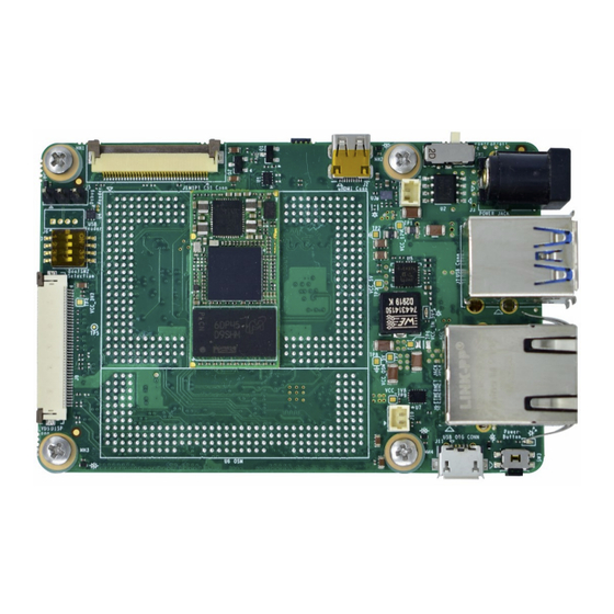
- Page 1 STM32MP13x SBC Hardware User Guide iW-RainboW-G54S STM32MP13x Single Board Computer Hardware User Guide REL0.1 iWave Systems Technologies Pvt. Ltd. Page 1 of 51 DRAFT VERSION SUBJECT TO CHANGE...
- Page 2 If you are not the intended recipient (or authorized to receive for the recipient), you are hereby notified that any disclosure, copying distribution or use of any of the information contained within this document is STRICTLY PROHIBITED. Thank you. “iWave Systems Tech. Pvt. Ltd.” REL0.1 iWave Systems Technologies Pvt.
- Page 3 No warranty of accuracy is given concerning the contents of the information contained in this publication. To the extent permitted by law no liability (including liability to any person by reason of negligence) will be accepted by iWave Systems, its subsidiaries or employees for any direct or indirect loss or damage caused by omissions from or inaccuracies in this document.
-
Page 4: Table Of Contents
STM32MP13x Pin Multiplexing on Expansion Connector ................40 TECHNICAL SPECIFICATION.......................... 45 Electrical Characteristics ..........................45 3.1.1 Power Input Requirement ........................... 45 Power Consumption............................46 EnvironmentalCharacteristics ......................... 47 3.3.1 Environmental Specification ........................47 REL0.1 iWave Systems Technologies Pvt. Ltd. Page 4 of 51 DRAFT VERSION SUBJECT TO CHANGE... - Page 5 3.3.2 RoHS Compliance ............................47 3.3.3 Electrostatic Discharge ..........................47 Mechanical Characteristics ..........................48 3.4.1 3.4.1 STM32MP13x SBC Mechanical Dimensions ..................48 ORDERING INFORMATION .......................... 50 REL0.1 iWave Systems Technologies Pvt. Ltd. Page 5 of 51 DRAFT VERSION SUBJECT TO CHANGE...
- Page 6 Figure 18: Mechanical Dimensions of STM32MP13x SBC Side View-1 ................48 Figure 19: Mechanical Dimensions of STM32MP13x SBC Bottom View ................ 49 Figure 20: Mechanical Dimensions of STM32MP13x SBC Side View-2 ................49 REL0.1 iWave Systems Technologies Pvt. Ltd. Page 6 of 51 DRAFT VERSION SUBJECT TO CHANGE...
- Page 7 Table 11: STM32MP13x SoC IOMUX for Expansion Connector Interfaces ..............40 Table 12: Power Input Requirement ..........................45 Table 13: Environmental Specification ........................... 47 Table 14: Orderable Product Part Numbers ........................50 REL0.1 iWave Systems Technologies Pvt. Ltd. Page 7 of 51 DRAFT VERSION SUBJECT TO CHANGE...
-
Page 8: Introduction
This document is the Hardware User Guide for the Single Board Computer based on the STMicroelectronics’s STM32MP13x Application processor. This board is fully supported by iWave Systems Technologies Pvt. Ltd. This Guide provides detailed information on the overall design and usage of the STMicroelectronics’s STM32MP13x SBC from a Hardware Systems perspective. - Page 9 Serial Audio Interface Secure Digital System on Chip Single Board Computer To Be Defined UART Universal Asynchronous Receiver/Transmitter Universal Serial Bus USB OTG USB On The Go REL0.1 iWave Systems Technologies Pvt. Ltd. Page 9 of 51 DRAFT VERSION SUBJECT TO CHANGE...
-
Page 10: Terminology Description
Note: Signal Type does not include internal pull-ups or pull-downs implemented by the chip vendors and only includes the pull-ups or pull-downs implemented on SBC. References • STM32MP131_Datasheet.pdf • STM32MP133_Datasheet.pdf • STM32MP135_Datasheet.pdf • STM32MP13_RM.pdf REL0.1 iWave Systems Technologies Pvt. Ltd. Page 10 of 51 DRAFT VERSION SUBJECT TO CHANGE... -
Page 11: Important Note
In this signal, BCONFIG_0 is the GPIO functionality which we are using and PA_0 is the GPIO number. Note: The above naming is not applicable for other signals which are not connected to CPU. REL0.1 iWave Systems Technologies Pvt. Ltd. Page 11 of 51 DRAFT VERSION SUBJECT TO CHANGE... -
Page 12: Architecture And Design
Note: These features are available only when using STM32MP133 or STM32MP135 MPU. There is no display support available in this SBC. mktg@iwavesystems.com iWave Systems Technologies Pvt. Ltd. Figure 1: STM32MP13x SBC Block Diagram REL0.1 iWave Systems Technologies Pvt. Ltd. Page 12 of 51... -
Page 13: Stm32Mp13X Sbc Features
UART x 2 Ports (without flow control) • SPI – 2 Ports • PWM – 5 Ports • ADC – 2 Ports • I2C3 – 1 Port REL0.1 iWave Systems Technologies Pvt. Ltd. Page 13 of 51 DRAFT VERSION SUBJECT TO CHANGE... - Page 14 Form Factor : 85mm x 56mm Memory Size will differ based on iWave’s SBC Product Part Number. eMMC is not populated in default configuration. Contact iWave if eMMC support is needed in the SBC. REL0.1 iWave Systems Technologies Pvt. Ltd.
-
Page 15: Cpu
Note: The STM32MP13x processor offers numerous advanced features, please refer the latest STM32MP13x Datasheet & Reference Manual for Electrical characteristics and other information, which may be revised from time to time. REL0.1 iWave Systems Technologies Pvt. Ltd. Page 15 of 51 DRAFT VERSION SUBJECT TO CHANGE... -
Page 16: Pmic
The STPMIC1EPQR comes in 44 pin WFQFN (5x6) Package and is placed on the Top side of the Module. REL0.1 iWave Systems Technologies Pvt. Ltd. Page 16 of 51 DRAFT VERSION SUBJECT TO CHANGE... -
Page 17: Memory
SDMMC2 controller of the STM32MP13x SoC and operates at 1.8V (I/O supply). The eMMC flash memory is physically located on bottom side of the SBC. The memory size of the eMMC Flash can be customised based on the requirement by contacting iWave Support Team. 2.6.4 Micro SD Connector The STM32MP13x SBC supports Micro SD slot which can be used to connect Micro SD card as an boot device as well as Mass storage device. -
Page 18: Boot Media Setting
Figure 4: Boot Media Switch Table 3: Boot Media Settings Boot Media POS3 POS2 POS1 (Force_Recov#) (BOOT_SEL1) (BOOT_SEL0) Serial NOR Flash (QSPI) SD Card (SDMMC1) UART/USB Boot REL0.1 iWave Systems Technologies Pvt. Ltd. Page 18 of 51 DRAFT VERSION SUBJECT TO CHANGE... -
Page 19: Network & Communication
Link/Activity (Green) LED indications on RJ45 Magjack. The RJ45 Magjack connector is physically located at the top of the board as shown below. Figure 5: Single RJ45 Magjack REL0.1 iWave Systems Technologies Pvt. Ltd. Page 19 of 51 DRAFT VERSION SUBJECT TO CHANGE... -
Page 20: Usb2.0 Otg Interface
This port can be used for USB OTG functionality which supports USB host and USB device based on the USB ID pin status. This USB2.0 OTG connector is physically located at the top of the board as shown below. Figure 6: USB OTG Connector REL0.1 iWave Systems Technologies Pvt. Ltd. Page 20 of 51 DRAFT VERSION SUBJECT TO CHANGE... -
Page 21: Usb Header
Pin Name Signal Name Description Termination VBUS_HOST_TP 5V, Power 5V Supply Voltage. I, USB Differential USB Negative. USB_DM1 Differential USB Positive. USB_DP1 I, USB Power Ground. REL0.1 iWave Systems Technologies Pvt. Ltd. Page 21 of 51 DRAFT VERSION SUBJECT TO CHANGE... -
Page 22: Serial Interface Features
Signal Type/ Pin Name Signal Name Description Termination UART4_TX(PD6) O, 3.3V CMOS UART interface Receive signal. UART4_RX(PD8) I, 3.3V CMOS UART interface Transmit signal. Power Ground. REL0.1 iWave Systems Technologies Pvt. Ltd. Page 22 of 51 DRAFT VERSION SUBJECT TO CHANGE... -
Page 23: Expansion Connector - 1
5V Supply Voltage. VCC_5V Power 5V Supply Voltage. VCC_5V Power 5V Supply Voltage. VCC_5V Power 5V Supply Voltage. Power Ground. VCC_5V Power 5V Supply Voltage. REL0.1 iWave Systems Technologies Pvt. Ltd. Page 23 of 51 DRAFT VERSION SUBJECT TO CHANGE... - Page 24 General purpose IO TIM1_CH2(PA9) PA9/D2 O, 1.8V PWM2 Signal GPIO_B_5(PD13) PD13/N1 IO, 1.8V General purpose IO SAI2_SCK_A_VD(PG1 PG12/L6 O, 1.8 SAI2 Serial clock Power Ground. REL0.1 iWave Systems Technologies Pvt. Ltd. Page 24 of 51 DRAFT VERSION SUBJECT TO CHANGE...
- Page 25 PA13/K7 IO, 1.8V BOOTFAIL_IN, Boot fail interrupt pin(connected to vendor define GPIO) GPIO_B_2(PA11) PA11/N5 IO, 1.8V General purpose IO Power Ground. Power Ground. Power Ground. REL0.1 iWave Systems Technologies Pvt. Ltd. Page 25 of 51 DRAFT VERSION SUBJECT TO CHANGE...
- Page 26 Signal Name CPU Ball Name/ Signal Type/ Description Pin No Pin Number Termination Power Ground. Power Ground. Power Ground. Power Ground. Power Ground. Power Ground. REL0.1 iWave Systems Technologies Pvt. Ltd. Page 26 of 51 DRAFT VERSION SUBJECT TO CHANGE...
-
Page 27: Expansion Connector - 2
Expansion Connector (J15) is physically located at the top of the SBC as shown below. Number of Pins : 100 Connector Part : TBD Figure 10: Expansion Connector-2 REL0.1 iWave Systems Technologies Pvt. Ltd. Page 27 of 51 DRAFT VERSION SUBJECT TO CHANGE... -
Page 28: Table 7: Expansion Connector-2 Pinouts
Power 12V Supply Voltage. VCC_12V Power 12V Supply Voltage. Power Ground. Power Ground. Power Ground. Power Ground. Power Ground. Power Ground. Power Ground. Power Ground. REL0.1 iWave Systems Technologies Pvt. Ltd. Page 28 of 51 DRAFT VERSION SUBJECT TO CHANGE... - Page 29 Signal Name CPU Ball Name/ Signal Type/ Description Pin No Pin Number Termination Power Ground. Power Ground. Power Ground. Power Ground. Power Ground. Power Ground. REL0.1 iWave Systems Technologies Pvt. Ltd. Page 29 of 51 DRAFT VERSION SUBJECT TO CHANGE...
- Page 30 SPI1 Master Chip Select 0. SPI1_MOSI(PA3) PA3/ T7 O, 1.8V CMOS SPI1 Master OUT and Slave IN. SPI1_MISO(PA6) PA6/ R8 I, 1.8V CMOS SPI1 Master IN and Slave OUT REL0.1 iWave Systems Technologies Pvt. Ltd. Page 30 of 51 DRAFT VERSION SUBJECT TO CHANGE...
-
Page 31: Expansion Connector - 3
Expansion Connector (J16) is physically located at the top of the SBC as shown below. Number of Pins : 100 Connector Part : TBD Figure 11: Expansion Connector-3 REL0.1 iWave Systems Technologies Pvt. Ltd. Page 31 of 51 DRAFT VERSION SUBJECT TO CHANGE... -
Page 32: Table 8: Expansion Connector-3 Pinouts
O, 1.8V SAI2 Master clock (PA12) Power Ground. SAI2_SD_B(PG3) PG3/U2 I, 1.8V SAI2 Data out SAI1_SCK_A(PC0) PC0/T4 I, 1.8V SAI1 clock Power Ground. Power Ground. REL0.1 iWave Systems Technologies Pvt. Ltd. Page 32 of 51 DRAFT VERSION SUBJECT TO CHANGE... - Page 33 SoC Tamper IN/OUT pin or UT4_RSVD1(PI2) General Purpose IO TAMP_IN8/TAMP_O SoC Tamper IN/OUT pin or UT1_RSVD2(PI0) General Purpose IO JTAG_TDO JTAG Data Out Signal Power Ground. JTAG_NJTRST JTAG Reset REL0.1 iWave Systems Technologies Pvt. Ltd. Page 33 of 51 DRAFT VERSION SUBJECT TO CHANGE...
- Page 34 JTAG Data In JTAG_TCK JTAG Clock JTAG_TMS JTAG TMS Power Ground. ADC2_INP8(PF11) ADC Analog Input ADC2_INP3(PA1) ADC Analog Input Power Ground. Power Ground. Power Ground. REL0.1 iWave Systems Technologies Pvt. Ltd. Page 34 of 51 DRAFT VERSION SUBJECT TO CHANGE...
- Page 35 STM32MP13x SBC Hardware User Guide Exp. Signal Name CPU Ball Name/ Signal Type/ Description Pin No Pin Number Termination Power Ground. Power Ground. REL0.1 iWave Systems Technologies Pvt. Ltd. Page 35 of 51 DRAFT VERSION SUBJECT TO CHANGE...
-
Page 36: Other Features
:10114829-10102LF from Amphenol ICC (FCI) Table 9: Fan Connector Pin Assignment Signal Type/ Pin No Signal Name Description Termination VCC_5V O, Power +5V Power output to FAN. Power Ground. REL0.1 iWave Systems Technologies Pvt. Ltd. Page 36 of 51 DRAFT VERSION SUBJECT TO CHANGE... -
Page 37: Rtc Battery Header
Pin No Signal Name Description Termination VRTC_3V0 I, Power +3V Power Input Power Ground. Note: Contact iWave support team if External RTC Controller support is required. REL0.1 iWave Systems Technologies Pvt. Ltd. Page 37 of 51 DRAFT VERSION SUBJECT TO CHANGE... -
Page 38: Power On/Off Switch
The STM32MP13x SBC has power ON/OFF switch (SW1) to control the Main power Input ON/OFF functionality. The Power ON/OFF switch is physically located at the top of the board as shown below. Figure 14: Power ON/OFF Switch REL0.1 iWave Systems Technologies Pvt. Ltd. Page 38 of 51 DRAFT VERSION SUBJECT TO CHANGE... -
Page 39: Reset Switch
Reset Push button switch to the reset signals of SoC and PMIC. This Reset Push button switch is physically located at the bottom of the board as shown below. Figure 15: Reset Switch REL0.1 iWave Systems Technologies Pvt. Ltd. Page 39 of 51 DRAFT VERSION SUBJECT TO CHANGE... -
Page 40: Stm32Mp13X Pin Multiplexing On Expansion Connector
This table has been prepared by referring STMicroelectronics STM32MP13x Hardware User’s Manual. Important Note: 1. It is strongly recommended to use the pin function same as selected in the SBC for iWave’s BSP reusability and to have compatible SBCs in future for upgradability. 2.Signals in blue are available in both 133 and 135. - Page 41 USART1_TX SAI1_CK2 LTDC_B6 1_NCS FMC_NE3 DCMIPP_D5 LTDC_B7 HDP_HDP6 TIM8_CH1 Expansion Connector-2 SPI1 DFSDM1_CKO I2S1_SDI/SPI1 I2S1_CK/SPI1 SAI1_MCLK_ ETH1_TX_C ETH2_TX_CL ADC1_INP13, I2S1_CK/SPI1_ SAI1_CK1 _MISO _SCK UART5_CTS ADC1_INN12 REL0.1 iWave Systems Technologies Pvt. Ltd. Page 41 of 51 DRAFT VERSION SUBJECT TO CHANGE...
- Page 42 I2S4_SDO/SPI4 QUADSPI_BK FMC_D3/FM I2S4_SDO/SPI4 I2C5_SCL _MOSI UART4_TX 1_NCS LTDC_B6 C_DA3 DCMIPP_D13 LTDC_G2 _MOSI TIM1_BKI SAI2_SCK_ UART4_DE/U RCC_MCO_2 TIM15_CH2 I2C3_SMBA SAI1_SCK_B ART4_RTS ETH2_TXD3 FMC_A22 DCMIPP_D7 LTDC_G3 REL0.1 iWave Systems Technologies Pvt. Ltd. Page 42 of 51 DRAFT VERSION SUBJECT TO CHANGE...
- Page 43 LPTIM3_OUT TIM15_CH1N USART2_RTS RX_CLK ADC2_INP3 ADC2_INP3 PF11 ADC1_INP8, ADC1_INN4, USART2_T DFSDM1_CKIN ADC2_INP8, SAI1_D2 SAI1_FS_A ETH2_RX_ER ADC2_INN4 ADC2_INP8 JTAG PF14 DEBUG_JTCK- SWCLK DEBUG_JTDI DEBUG_JTDO- NJTRST DEBUG_JTRST REL0.1 iWave Systems Technologies Pvt. Ltd. Page 43 of 51 DRAFT VERSION SUBJECT TO CHANGE...
- Page 44 ETH2_REF_ I2S2_WS/SPI2 QUADSPI_BK CLK/ETH2_ SPI5_NSS TIM5_CH2 SAI2_SD_A _NSS I2C4_SCL USART6_RX 2_IO0 RX_CLK FMC_A12 LTDC_G6 SAI2_SD_A ETH2_GTX_C ETH1_MDI TIM8_BKIN2 I2C2_SDA SAI2_SD_B FDCAN2_RX FMC_A13 DCMIPP_D15 DCMIPP_D12 SAI2_SD_B REL0.1 iWave Systems Technologies Pvt. Ltd. Page 44 of 51 DRAFT VERSION SUBJECT TO CHANGE...
-
Page 45: Technical Specification
12.25V ±50mV VRTC_3V0 2.8V 3.3V ±20mV ¹ The STM32MP13x SBC uses this voltage as backup power source to SoC VBAT pin when VCC is off. REL0.1 iWave Systems Technologies Pvt. Ltd. Page 45 of 51 DRAFT VERSION SUBJECT TO CHANGE... -
Page 46: Power Consumption
STM32MP13x SBC Hardware User Guide Power Consumption REL0.1 iWave Systems Technologies Pvt. Ltd. Page 46 of 51 DRAFT VERSION SUBJECT TO CHANGE... -
Page 47: Environmentalcharacteristics
3.3.3 Electrostatic Discharge iWave’s STM32MP13x SBC is sensitive to electro static discharge and so high voltages caused by static electricity could damage some of the devices on board. It is packed with necessary protection while shipping. Do not open or use the SBC except at an electrostatic free workstation. -
Page 48: Mechanical Characteristics
Connector), followed by Dual Ethernet Connector (16.40mm). In bottom side maximum height component is JTAG connector (5.91mm) followed by M.2 SMT spacer (3.99mm). Figure 18: Mechanical Dimensions of STM32MP13x SBC Side View-1 REL0.1 iWave Systems Technologies Pvt. Ltd. Page 48 of 51 DRAFT VERSION SUBJECT TO CHANGE... -
Page 49: Figure 19: Mechanical Dimensions Of Stm32Mp13X Sbc Bottom View
STM32MP13x SBC Hardware User Guide Figure 19: Mechanical Dimensions of STM32MP13x SBC Bottom View Figure 20: Mechanical Dimensions of STM32MP13x SBC Side View-2 REL0.1 iWave Systems Technologies Pvt. Ltd. Page 49 of 51 DRAFT VERSION SUBJECT TO CHANGE... -
Page 50: Ordering Information
The below table provides the standard orderable part numbers for different STM32MP13x SBC variations. Please contact iWave for orderable part number of higher RAM memory size or Flash memory size SBC configurations. Also, if the desired part number is not listed in below table or if any custom configuration part number is required, please contact iWave. -
Page 51: Iwave Systems Technologies Pvt. Ltd
STM32MP13x SBC Hardware User Guide REL0.1 iWave Systems Technologies Pvt. Ltd. Page 51 of 51 DRAFT VERSION SUBJECT TO CHANGE...
Need help?
Do you have a question about the STM32MP13 Series and is the answer not in the manual?
Questions and answers