
Related Manuals for iWave iW-RainboW-G25M


Summary of Contents for iWave iW-RainboW-G25M
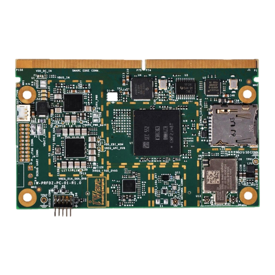
- Page 1 Snapdragon 820 SMARC SOM Hardware User Guide iW-RainboW-G25M Snapdragon 820 SMARC SOM Hardware User Guide DRAFT VERSION SUBJECT TO CHANGE REL0.1 iWave Systems Technologies Pvt. Ltd. Page 1 of 52...
- Page 2 If you are not the intended recipient (or authorized to receive for the recipient), you are hereby notified that any disclosure, copying distribution or use of any of the information contained within this document is STRICTLY PROHIBITED. Thank you. “iWave Systems Tech. Pvt. Ltd.” REL0.1 iWave Systems Technologies Pvt.
- Page 3 No warranty of accuracy is given concerning the contents of the information contained in this publication. To the extent permitted by law no liability (including liability to any person by reason of negligence) will be accepted by iWave Systems, its subsidiaries or employees for any direct or indirect loss or damage caused by omissions from or inaccuracies in this document.
-
Page 4: Table Of Contents
2.9.1 JTAG Header ............................43 2.9.2 Debug UART Header ..........................44 2.9.3 Battery Connector ..........................44 2.9.4 Audio In/Out Jack ........................... 45 2.9.5 UFS - Universal Flash Storage ......................... 45 REL0.1 iWave Systems Technologies Pvt. Ltd. Page 4 of 52... - Page 5 3.2.3 Electrostatic Discharge ........................... 48 Mechanical Characteristics ........................49 3.3.1 Snapdragon 820 SMARC SOM Mechanical Dimensions ................49 ORDERING INFORMATION ..........................50 APPENDIX ................................. 51 Snapdragon 820 SMARC SOM Development Platform ................51 REL0.1 iWave Systems Technologies Pvt. Ltd. Page 5 of 52...
- Page 6 Table 8: Battery Connector Pin Out ........................... 44 Table 9: Power Input Requirement ..........................46 Table 10: Power Sequence Timing ..........................47 Table 11: Environmental Specification........................48 Table 12: Orderable Product Part Numbers ....................... 50 REL0.1 iWave Systems Technologies Pvt. Ltd. Page 6 of 52...
-
Page 7: Introduction
This document is the Hardware User Guide for the Snapdragon 820 SMARC SOM based on the Qualcomm APQ8096 Application processor. This board is fully supported by iWave Systems Technologies Pvt. Ltd. This Guide provides detailed information on the overall design and usage of the Snapdragon 820 SMARC SOM from a Hardware Systems perspective. - Page 8 Smart Mobility ARChitecture SPMI Serial power management interface To Be Defined UART Universal Asynchronous Receiver/Transmitter Universal Flash Storage Universal Serial Bus USB OTG USB On The Go Voltage Wi-Fi Wireless Fidelity REL0.1 iWave Systems Technologies Pvt. Ltd. Page 8 of 52...
-
Page 9: Terminlogy Description
Note: Signal Type does not include internal pull-ups or pull-downs implemented by the chip vendors and only includes the pull-ups or pull-downs implemented On-SMARC SOM. References • APQ8096 Hardware User Manuals. • SMARC Specification V2.0 REL0.1 iWave Systems Technologies Pvt. Ltd. Page 9 of 52... -
Page 10: Important Note
If CPU pin doesn’t have multiplexing option, then the signal name is mentioned as, “Function name” Example: SPMI_CLK In this signal, functionality which we are using SPMI_CLK Note: The above naming is not applicable for other signals which are not connected to CPU. REL0.1 iWave Systems Technologies Pvt. Ltd. Page 10 of 52... -
Page 11: Architecture And Design
2. ARCHITECTURE AND DESIGN This section provides detailed information about the Snapdragon 820 SMARC SOM features and Hardware architecture with high level block diagram. Snapdragon 820 SMARC SOM Block Diagram iW-RainboW-G25M - APQ8096 SMARC SOM Block Diagram Gigabit PCIe Ethernet... -
Page 12: Snapdragon 820 Smarc Som Features
SPI x 2 Port • USB2.0 x 2 Port • USB3.0 x 2 Port • USB OTG x 1 Port • PCIe x 1 Port • HDMI x 1 Port REL0.1 iWave Systems Technologies Pvt. Ltd. Page 12 of 52... - Page 13 UFS (Universal Flash Storage) • Debug UART Header • Battery Connector • JTAG Header General Specification • Power Supply : 5V,3A • Form Factor : 82mm X 50mm (SMARC V2.0 Specification) REL0.1 iWave Systems Technologies Pvt. Ltd. Page 13 of 52...
-
Page 14: Qualcomm Apq8096 Cpu
Adreno 430. Note: Please refer the latest APQ8096 Datasheet & Reference Manual for Electrical characteristics and other information related to APQ8096 CPU which may be revised from time to time. REL0.1 iWave Systems Technologies Pvt. Ltd. Page 14 of 52... -
Page 15: Power Management
The eMMC flash (U24) memory is physically located on bottom side of the SMARC SOM. The memory size of the eMMC Flash can be expandable and the APQ8096 CPU supports eMMC version 5.1V REL0.1 iWave Systems Technologies Pvt. Ltd. Page 15 of 52... -
Page 16: Micro Sd Connector Slot
SD Interface Data Line0. DAT1 SDC4_DATA_1(GPIO_95) IO 1.8 V CMOS SD Interface Data Line1. SDC4_CD_N(GPIO_26) I, 1.8V CMOS SD Interface Card Detect. /1M PU Power Ground. Power Ground. Power Ground. Power Ground. REL0.1 iWave Systems Technologies Pvt. Ltd. Page 16 of 52... -
Page 17: Network & Communiation
WLAN/BT and ANT2 is for WLAN only. MHF-4 Micro RF Coaxl connectors are used for interfacing the RF antenna as shown below. Example of RF connector P/N: 20449-001E (MHF-4). Figure 3: WLAN/BT Antenna Connector REL0.1 iWave Systems Technologies Pvt. Ltd. Page 17 of 52... -
Page 18: Gps Interface
GLONASS and COMPASS operations. RF antenna need to be connected for better GPS locking function. MHF-4 Micro R Coax connector is used for interfacing the GPS antenna (J7) as shown in below figure. Figure 4: GPS Antenna Connector REL0.1 iWave Systems Technologies Pvt. Ltd. Page 18 of 52... -
Page 19: Smarc Pcb Edge Connector
314pin SMARC Edge connector are explained in the following sections. Figure 5: SMARC Edge Connector Number of Pins - : 314 Connector Part - : Not Applicable (On Board PCB Edge connector) Mating Connector - : 91782-3140M-001 from Aces REL0.1 iWave Systems Technologies Pvt. Ltd. Page 19 of 52... -
Page 20: Gigabit Ethernet
SPI0 and ESPI channels from the SMARC Edge connector with BLSP1_SPI and BLSP1_SPI respectively. For more details on SMARC Edge SPI pinouts, refer SAMRC Edge connector pins P43, P44, P45, P46, P31, P54, P55, P56, P57 & P58 on Table 6. REL0.1 iWave Systems Technologies Pvt. Ltd. Page 20 of 52... -
Page 21: Usb Interface
For more details on SMARC Edge DSI pinouts, refer SAMRC Edge connector S107, S108, S109, S111, S112, S114, S115, S116, S117, S118, S120, S121, S122, S125, S126, S127, S128, S129, S131, S132, S133, S134, S135, S137, S138, S139, S140 & S141 on Table 6. REL0.1 iWave Systems Technologies Pvt. Ltd. Page 21 of 52... -
Page 22: Mipi Csi Camera
SMARC V2.0 specification supports System and Power & Management Signals. For more details on SMARC Edge Power & Management Signals pinouts, refer SAMRC Edge connectorP123, P124, P125, P126, P127, P128, S145, S147, S150, S153, S154 & S155 pins on Table 6. REL0.1 iWave Systems Technologies Pvt. Ltd. Page 22 of 52... -
Page 23: Table 4: 314-Pin Pcb Edge Connector Pin Assignment
Gigabit Ethernet link status GBE0_LINK1000# O, 3.3V CMOS Gigabit Ethernet MDI GBE0_MDI2- GBE0_MDI2- IO, DIFF differential pair 2 negative. Gigabit Ethernet MDI GBE0_MDI2+ GBE0_MDI2+ IO, DIFF differential pair 2 positive. REL0.1 iWave Systems Technologies Pvt. Ltd. Page 23 of 52... - Page 24 SPI0_CS0# O, 1.8V CMOS SPI0 Chip Select 0 N(GPIO_2) BLSP1_SPI_CLK( GPIO_3/ SPI0_CK O, 1.8V CMOS SPI0 Clock GPIO_3) BLSP1_SPI_MIS GPIO_1/ SPI0_DIN I, 1.8V CMOS SPI0 Master IN Slave Out O(GPIO_1) REL0.1 iWave Systems Technologies Pvt. Ltd. Page 24 of 52...
- Page 25 USB Port1 Power Enable/ USB1_EN_OC# USB_HUB3_OC IO, 3.3V CMOS Over Current Indicator Note: Connected to USB Hub Power Ground. USB_HUB1OUT_ USB Port2 Data Positive USB2+ IO, DIFF Note: Connected to USB Hub REL0.1 iWave Systems Technologies Pvt. Ltd. Page 25 of 52...
- Page 26 PCIE1_RX_M I, Diff PCIE1 Receive Negative Power Ground. O, Diff/ PCIE1_TX_P/ PCIE_A_TX+ PCIE1_TX_P 0.1uF AC PCIE1 Transmit Positive Couple O, Diff/ PCIE1_TX_M/ PCIE_A_TX- PCIE1_TX_M 0.1uF AC PCIE1 Transmit Negative Couple REL0.1 iWave Systems Technologies Pvt. Ltd. Page 26 of 52...
- Page 27 SMARC General Purpose P112 GPIO4 / HDA_RST# IO, 1.8V CMOS (GPIO_100) AP46 Input/output 4 SMARC General Purpose SMARC_GPIO_5 P113 GPIO5 / PWM_OUT IO, 1.8V CMOS Input/output 5 (PM_GPIO4) Note: Connected to PMIC REL0.1 iWave Systems Technologies Pvt. Ltd. Page 27 of 52...
- Page 28 Clear to Send S_N(GPIO_51) BD52 P133 Power Ground. BLSP10_UART_T GPIO_8/ P134 SER1_TX O, 1.8V CMOS BLSP10_UART Transmitter X(GPIO_8) BF50 BLSP10_UART_R GPIO_9/ P135 SER1_RX I, 1.8V CMOS BLSP10_UART Receiver X(GPIO_9) BG51 REL0.1 iWave Systems Technologies Pvt. Ltd. Page 28 of 52...
- Page 29 MIPI CSI0 I2C Clock I2C_CAM0_CK PIO_18) CLK1_OUT(GPIO GPIO_13/ CAM_MCK O, 1.8V CMOS Master Clock for Camera _13) CSI0_TX+ / CCI_I2C0_SDA(G GPIO_17/ IO, 1.8V CMOS MIPI CSI0 I2C Data I2C_CAM0_DAT PIO_17) REL0.1 iWave Systems Technologies Pvt. Ltd. Page 29 of 52...
- Page 30 Note: Connected to USB Hub USB3_VBUS_DET MI2S_2_MCLK( GPIO_79/ AUDIO_MCK O, 1.8V CMOS Master Clock for Audio codec GPIO_79) MI2S_2_WS(GPI GPIO_81/ I2S0_LRCK O, 1.8V CMOS I2S Channel0 Left Right Clock O_81) REL0.1 iWave Systems Technologies Pvt. Ltd. Page 30 of 52...
- Page 31 Note: Connected to USB Hub USB3.0 Port3 Transmit USB3_HUB2_TX USB3_SSTX- O, DIFF Negative Note: Connected to USB Hub Power Ground. USB3.0 Port3 Receive USB3_HUB2_RX USB3_SSRX+ I, DIFF Positive Note: Connected to USB Hub REL0.1 iWave Systems Technologies Pvt. Ltd. Page 31 of 52...
- Page 32 AV46 PCIE_C_RX+ Note: Optionally connected to PCIE0_RX_P PCIE_C_RX- Note: Optionally connected to PCIE0_RX_M Power Ground. PCIE_C_TX+ Note: Optionally connected to PCIE0_TX_P PCIE_C_TX- Note: Optionally connected to PCIE0_TX_M Power Ground. PCIE_B_REFCK+ REL0.1 iWave Systems Technologies Pvt. Ltd. Page 32 of 52...
- Page 33 MIPI_DSI1_CLK_ MIPI_DSI1_CLK_P/ MIPI DSI1 differential clock S108 eDP1_AUX+ / O, DIFF BE31 positive DSI1_CLK+ LVDS1_CK- / MIPI_DSI1_CLK_ MIPI_DSI1_CLK_N/ MIPI DSI1 differential clock S109 eDP1_AUX- / O, DIFF BF32 negative DSI1_CLK- REL0.1 iWave Systems Technologies Pvt. Ltd. Page 33 of 52...
- Page 34 LVDS0_0- / MIPI_DSI0_LN0 MIPI_DSI0_LN0_N/ MIPI DSI0 differential data S126 eDP0_TX0- / O, DIFF BJ37 lane 0 negative DSI0_D0- LCD0_BKLT_EN( GPIO_119/ S127 LCD0_BKLT_EN O, 1.8V CMOS LCD0 Backlight Enable GPIO_119) AR51 REL0.1 iWave Systems Technologies Pvt. Ltd. Page 34 of 52...
- Page 35 LCD0_BKLT_PWM O, 1.8V CMOS control PWM M(PM_GPIO3) Note: from PMIC S142 RSVD9 S143 Power Ground. S144 eDP0_HPD WDT_TIME_OU GPIO_101/ Watch DOG Time Out S145 WDT_TIME_OUT# O, 1.8V CMOS AT52 Interrupt REL0.1 iWave Systems Technologies Pvt. Ltd. Page 35 of 52...
- Page 36 Client Mode when in the Force Recovery function is invoked. S156 BATLOW# I, 1.8V CMOS Module vendor specific test S157 TEST# TEST# 10K PU is not supported. S158 Power Ground. REL0.1 iWave Systems Technologies Pvt. Ltd. Page 36 of 52...
-
Page 37: Expansion Connector
SOM. Figure 6: SMARC Expansion Connector Number of Pins - : 100 Connector Part - : FX8C-100S-SV(91) from Hirose Mating Connector - : FX8C-100P-SV(91) from Hirose REL0.1 iWave Systems Technologies Pvt. Ltd. Page 37 of 52... -
Page 38: Table 5: Expansion Connector Pin Assignment
Note: On SOM Audio Codec is not supported by default Power Ground. EXP_HPH_R Note: On SOM Audio Codec is not supported by default USB3.0 Port3 Transmit Positive USB3_HUB4_TXP I, DIFF Note: Connected to USB Hub REL0.1 iWave Systems Technologies Pvt. Ltd. Page 38 of 52... - Page 39 Power Ground. Power Ground. HSDET_L Note: On SOM Audio Codec is not supported by default AMIC3_INP Note: On SOM Audio Codec is not supported by default Power Ground. REL0.1 iWave Systems Technologies Pvt. Ltd. Page 39 of 52...
- Page 40 GPIO_12/ GPIO_12 IO, 1.8V CMOS General Purpose Input / Output BJ45 EXP_SLIMBUS_CLK(GPIO_7 GPIO_70/ IO, 1.8V CMOS SLIMBUS Clock SSC_14/ SSC_UART_2_TX (SSC_14) IO, 1.8V CMOS Sensor Core UART2 Transmitter Power Ground. REL0.1 iWave Systems Technologies Pvt. Ltd. Page 40 of 52...
- Page 41 GPIO_27/ BLSP6_I2C_SDA(GPIO_27) IO, 1.8V CMOS BLSP6 I2C2 Data GPIO_22/ GPIO_22 IO, 1.8V CMOS General Purpose Input / Output Power Ground. GPIO_24/ GPIO_24 IO, 1.8V CMOS General Purpose Input / Output REL0.1 iWave Systems Technologies Pvt. Ltd. Page 41 of 52...
- Page 42 MIPI_CSI2_DCLK_P I, DIFF MIPI CSI2 differential Clock positive /BF2 MIPI_CSI2_DLN3_ MIPI CSI2 differential data lane 3 MIPI_CSI2_DLN3_M I, DIFF M/AY2 negative MIPI_CSI2_DCLK_ MIPI CSI2 differential Clock MIPI_CSI2_DCLK_M I, DIFF negative REL0.1 iWave Systems Technologies Pvt. Ltd. Page 42 of 52...
-
Page 43: Optional Features
JTAG_TDO O, 1.8V CMOS JTAG test data output. Power Ground. JTAG_RESETB I, 1.8V CMOS/ Reset input. 10K PU Power Ground. I, 1.8V CMOS/ Only pull up is provided. 10K PU REL0.1 iWave Systems Technologies Pvt. Ltd. Page 43 of 52... -
Page 44: Debug Uart Header
Table 8: Battery Connector Pin Out Signal Type/ Pin Name Signal Name Description Termination VBATT VBATT I, 3.6 ~ 4.35V Battery input pin BATT_THERM BATT_THERM Battery thermal sense pin. Power Ground REL0.1 iWave Systems Technologies Pvt. Ltd. Page 44 of 52... -
Page 45: Audio In/Out Jack
JEDEC specification for Universal Flash Storage (UFS)(JESD220B) –v2.0, JEDEC specification for UFS Host Controller Interface(JESD223A) –v2.0, MIPI Alliance specification for Unified Protocol(UniPro) –v1.6.00 and MIPI Alliance specification for M-PHY–v3Audio/Video Feature The UFS(U23) memory is physically located on bottom side of the SMARC SOM Contact iWave Support team for further information. REL0.1 iWave Systems Technologies Pvt. -
Page 46: Technical Specification
Sl. No. Power Rail Min (V) Typical (V) Max(V) Max Input Ripple VDD_IN 4.2V 5.25 ±50mV ¹ VDD_IN pin can be powered from either SMRAC Carrier Card or External power source. REL0.1 iWave Systems Technologies Pvt. Ltd. Page 46 of 52... -
Page 47: Power Input Sequencing
SOM Power rise time to CARRIER_PWR_ON rise time ≥ 0 ms CARRIER_PWR_ON rise time to CARRIER_STBY# rise time ≥ 0 ms CARRIER_STBY# rise time to CARRIER POWER rise time 100 to 500ms 3.1.2 Power Consumption REL0.1 iWave Systems Technologies Pvt. Ltd. Page 47 of 52... -
Page 48: Environmental Characteristics
3.2.3 Electrostatic Discharge iWave’s Snapdragon 820 SMARC SOM is sensitive to electro static discharge and so high voltages caused by static electricity could damage some of the devices on board. It is packed with necessary protection while shipping. Do not open or use the SOM except at an electrostatic free workstation. -
Page 49: Mechanical Characteristics
IC U25 (1.2mm). Please refer the below figure which gives height details of the Snapdragon 820 SMARC SOM. Figure 9: Mechanical dimension of Snapdragon 820 SMARC SOM- Side View REL0.1 iWave Systems Technologies Pvt. Ltd. Page 49 of 52... -
Page 50: Ordering Information
The below table provides the standard orderable part numbers for different Snapdragon 820 SMARC SOM variations. Please contact iWave for orderable part number of higher RAM memory size or Flash memory size SOM configurations. Also, if the desired part number is not listed in below table or if any custom configuration part number is required, please contact iWave. -
Page 51: Appendix
5. APPENDIX Snapdragon 820 SMARC SOM Development Platform iWave Systems supports iW-RainboW-G25D – Snapdragon 820 SMARC SOM Development Platform which is targeted for quick validation of Snapdragon 820 CPU based SMARC SOM and its features. Being a Nano-ITX form factor with 120mm x 120mm size, the carrier board is highly packed with all necessary interfaces &... - Page 52 Snapdragon 820 SMARC SOM Hardware User Guide REL0.1 iWave Systems Technologies Pvt. Ltd. Page 52 of 52...
Need help?
Do you have a question about the iW-RainboW-G25M and is the answer not in the manual?
Questions and answers