
Related Manuals for iWave iW-RainboW-G23S


Summary of Contents for iWave iW-RainboW-G23S
- Page 1 RZ/G1C SBC Hardware User Guide iW-RainboW-G23S RZ/G1C Single Board Computer Hardware User Guide REL1.1 iWave Systems Technologies Pvt. Ltd. Page 1 of 51...
- Page 2 If you are not the intended recipient (or authorized to receive for the recipient), you are hereby notified that any disclosure, copying distribution or use of any of the information contained within this document is STRICTLY PROHIBITED. Thank you. “iWave Systems Tech. Pvt. Ltd.” REL1.1 iWave Systems Technologies Pvt.
- Page 3 (including liability to any person by reason of negligence) will be accepted by iWave Systems, its subsidiaries or employees for any direct or indirect loss or damage caused by omissions from or inaccuracies in this document.
-
Page 4: Table Of Contents
Expansion Connector2 (40 Pin) Interfaces ...................... 32 2.10.1 LVDS Interface ............................. 33 2.10.2 CAN Interface .............................. 33 2.10.3 I2S Audio Interface ............................33 2.10.4 Data UART Interface ........................... 34 2.10.5 I2C Interface ..............................34 REL1.1 iWave Systems Technologies Pvt. Ltd. Page 4 of 51... - Page 5 3.2.3 Electrostatic Discharge ..........................47 Mechanical Characteristics ..........................48 3.3.1 RZ/G1C SBC Mechanical Dimensions ......................48 ORDERING INFORMATION .......................... 49 APPENDIX I ..............................50 5.1.1 RZ/G1C SPI Programmer Board ........................50 REL1.1 iWave Systems Technologies Pvt. Ltd. Page 5 of 51...
- Page 6 Table 13: Power Input Requirement ..........................45 Table 14: Power Output Specification ..........................46 Table 15: Power Consumption ............................46 Table 16: Environmental Specification ........................... 47 Table 17: Orderable Product Part Numbers ........................49 REL1.1 iWave Systems Technologies Pvt. Ltd. Page 6 of 51...
-
Page 7: Introduction
This document is the Hardware User Guide for the RZ/G1C Single Board Computer based on the Renesas’s RZ/G1C Application processor. This board is fully supported by iWave Systems Technologies Pvt. Ltd. This guide provides detailed information on the overall design and usage of the RZ/G1C SBC from a Hardware Systems perspective. - Page 8 Serial Communication Interface with FIFO Secure Digital SDHI SD Card Host Interface Serial Sound Interface SDRAM Synchronous Dynamic Random Access Memory UART Universal Asynchronous Receiver/Transmitter Universal Serial Bus USB OTG USB On The Go REL1.1 iWave Systems Technologies Pvt. Ltd. Page 8 of 51...
-
Page 9: Terminlogy Description
Note: Signal Type does not include internal pull-ups or pull-downs implemented by the chip vendors and only includes the pull-ups or pull-downs implemented On-SBC. References • RZ/G1C CPU Hardware User Manual REL1.1 iWave Systems Technologies Pvt. Ltd. Page 9 of 51... -
Page 10: Important Note
“Function name” Example: TXOUT0M In this signal, functionality which we are using is LVDS TXOUT0M Note: The above naming is not applicable for other signals which are not connected to CPU. REL1.1 iWave Systems Technologies Pvt. Ltd. Page 10 of 51... -
Page 11: Architecture And Design
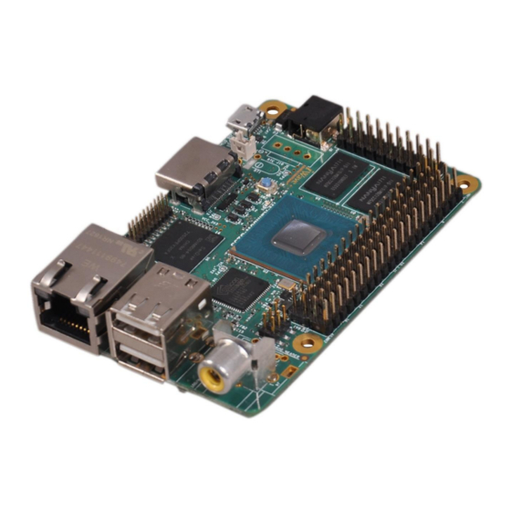
This section provides detailed information about the RZ/G1C SBC features and Hardware architecture with high level block diagram. Also, this section provides detailed information about SBC Expansion connectors pin assignment and usage. RZ/G1C SBC Block Diagram iW-RainboW-G23S - RZ/G1C SBC Block Diagram 40Pin 40Pin SPI Programming... -
Page 12: Rz/G1C Sbc Features
• JTAG Header • Reset Switch Expansion Connector1 (40 Pin) Interfaces • Data UART (without CTS & RTS) x 1 • SPI x1 • I2C x 2 • GPIOs (17nos) REL1.1 iWave Systems Technologies Pvt. Ltd. Page 12 of 51... - Page 13 RZ/G1C CPU supports one CVBS Video IN and one CVBS Video Out port. By default CVBS Video IN port is supported on RZ/G1C SBC. To support CVBS Video Out port, contact iWave. Expansion connector1 pinout is compatible with Raspberry Pi3 connector pinout.
-
Page 14: Rz/G1C Cpu
1 GHz/core. The Block Diagram of RZ/G1C CPU from Renesas’s website is shown below for reference. Figure 2: RZ/G1C CPU Simplified Block Diagram Note: Please refer the latest RZ/G1C Hardware User Manual for more details which may be revised from time to time. REL1.1 iWave Systems Technologies Pvt. Ltd. Page 14 of 51... -
Page 15: Boot Media Setting Switch
Figure 3: Boot Media Switch Table 3: Boot Media Settings SW1 (2 Position Switch) Boot Media Setting On RZ/G1C SBC POS1 POS2 Image QSPI0 - SPI Flash (Default) MMC0 - 8bit eMMC REL1.1 iWave Systems Technologies Pvt. Ltd. Page 15 of 51... -
Page 16: Memory
The SPI flash memory is physically located on bottom side of the SBC. To program the boot code in to the SPI flash (for the first time or if boot code is corrupted), use iWave’s RZ/G1C SPI Programmer Board through SPI Flash Programming Header (J6) (or) JTAG debugger through JTAG Header (J14). -
Page 17: Micro Sd Connector
GP2_24. If GP2_24 is set to low, then 1.8V IO level is selected for SDHI2 lines. If GP2_24 is set to high, then 3.3V IO level is selected for SDHI2 lines. Micro SD Connector is physically located on bottom side of the SBC as shown below. Figure 4: Micro SD Connector REL1.1 iWave Systems Technologies Pvt. Ltd. Page 17 of 51... -
Page 18: Communication Features
RZ/G1C SBC also supports Activity (Yellow) and Link (Green) LED indications on RJ45 Magjack. The 100/1000 Mbps Ethernet Connector is physically located on top side of the SBC as shown below. Figure 5: Gigabit Ethernet Connector REL1.1 iWave Systems Technologies Pvt. Ltd. Page 18 of 51... -
Page 19: Dual Usb 2.0 Host Ports
500mA. Also over current output & power enable input of the current limit power switch is connected to corresponding USB HUB port’s control pins to control the USB ports VBUS power. Figure 6: Dual USB 2.0 Host Connector REL1.1 iWave Systems Technologies Pvt. Ltd. Page 19 of 51... -
Page 20: Usb 2.0 Device Port
Micro B Connector is connected to RZ/G1C CPU’s GPIO “GP0_1” pin. The Micro B Connector (J15) is physically located on top side of the SBC as shown below. Figure 7: USB 2.0 Device Connector REL1.1 iWave Systems Technologies Pvt. Ltd. Page 20 of 51... -
Page 21: Video Features
HDMI transmitter output is connected to Standard HDMI connector with ESD protection circuitry. HDMI Output connector (J13) is physically located on top of the SBC as shown below. Figure 8: HDMI Connector REL1.1 iWave Systems Technologies Pvt. Ltd. Page 21 of 51... -
Page 22: Cvbs Input Port
Video DAC. It supports NTSC, PAL, PAL-M, PAL-N, and PAL-60 encode processing. The output of the Video DAC is directly connected to RCA JACK and by default not populated. REL1.1 iWave Systems Technologies Pvt. Ltd. Page 22 of 51... -
Page 23: Other Features
Figure 10: RTC Battery Connector Table 4: RTC Battery Connector Pin Assignment Signal Type/ Signal Name Description Termination VBAT+ I, 3.0V Power RTC Coin Cell Power input. VBAT- Power Ground. REL1.1 iWave Systems Technologies Pvt. Ltd. Page 23 of 51... -
Page 24: Spi Flash Programming Header
2.8.2 SPI Flash Programming Header To program the boot code in to the SPI flash (for the first time or if boot code is corrupted), use iWave’s RZ/G1C SPI Programmer Board through 6pin SPI Flash Programming Header (J6) (or) JTAG debugger through JTAG Header (J14). -
Page 25: Jtag Header
SBC as shown below. Figure 12: JTAG Header Number of Pins - 20 Connector Part Number - 62132021021 Mating Connector - LPPB102CFFN-RC from Sullins Connector Solutions REL1.1 iWave Systems Technologies Pvt. Ltd. Page 25 of 51... -
Page 26: Table 6: Jtag Header Pin Assignment
JTAG test data Output. Power Ground. JTAG_RESETB JTAG_RESETB I, 1.8V CMOS/ JTAG reset Signal. 1K PU Power Ground. Power Ground. I, 1.8V CMOS/ Only pull down is provided. 10K PD Power Ground. REL1.1 iWave Systems Technologies Pvt. Ltd. Page 26 of 51... -
Page 27: Reset Switch
The RZ/G1C SBC supports Push button switch (SW2) to reset the RZ/G1C CPU. This Reset Push button switch (SW2) is physically located at the top of the SBC as shown below. Figure 13: Reset Switch REL1.1 iWave Systems Technologies Pvt. Ltd. Page 27 of 51... -
Page 28: Expansion Connector1 (40 Pin) Interfaces
Note: This connector pinout is compatible with Raspberry Pi3 connector pinout. Number of Pins - 40 Connector Part Number - 61304021121 Mating Connector - 61304021821 from Wurth Electronics Staking Height - 6mm REL1.1 iWave Systems Technologies Pvt. Ltd. Page 28 of 51... -
Page 29: Data Uart Interface
For more details, refer Expansion Connector1 Pins 7, 11, 12, 13, 15, 16, 18, 22, 29, 31, 32, 33, 35, 36, 37, 38 & 40 for GPIOs on Table 7. REL1.1 iWave Systems Technologies Pvt. Ltd. Page 29 of 51... -
Page 30: Table 7: Expansion Connector1 Pin Assignment
IO, 3.3V CMOS General purpose input/output. MSIOF2_TXD_A(GP1_11) D11/ O,3.3V CMOS SPI Master serial output/Slave serial input (MSIOF2). Power Ground. MSIOF2_RXD_A(GP1_10) D10/ I,3.3V CMOS SPI Master serial input /Slave serial output (MSIOF2). REL1.1 iWave Systems Technologies Pvt. Ltd. Page 30 of 51... - Page 31 GPIO(GP1_20) QSPI0_IO3/ IO, 3.3V CMOS General purpose input/output. Note: GP1_20 is connected to this pin through resistor and default populated. Power Ground. GPIO(GP5_0) SSI_SCK5_A/ IO, 3.3V CMOS General purpose input/output. REL1.1 iWave Systems Technologies Pvt. Ltd. Page 31 of 51...
-
Page 32: Expansion Connector2 (40 Pin) Interfaces
Expansion Connector2 (J3) is physically located at the top of the SBC as shown below. Figure 15: Expansion Connector2 Number of Pins - 40 Connector Part Number - 61304021121 Mating Connector - 61304021821 from Wurth Electronics Staking Height - 6mm REL1.1 iWave Systems Technologies Pvt. Ltd. Page 32 of 51... -
Page 33: Lvds Interface
297.3kHz to 15.1 MHz at slave mode. SSI Module supports TDM format operation at 44.1 or 48kHz sampling rate. For more details, refer Expansion connector2 pins 1, 3 & 5 for SSI1 and 6, 8, 10 & 12 for SSI0/9 on Table 8. REL1.1 iWave Systems Technologies Pvt. Ltd. Page 33 of 51... -
Page 34: Data Uart Interface
× 1024 cycles of internal bus clock (i.e. from 30.77 ns to 264 seconds when bus clock = 65 MHz). Also it supports continuous pulse output mode or single pulse output mode which is configurable. For more details, refer Expansion connector2 pin 40 for PWM0 on Table 8. REL1.1 iWave Systems Technologies Pvt. Ltd. Page 34 of 51... -
Page 35: Table 8: Expansion Connector2 Pin Assignment
Interface (HSCIF2) Ready to Send. TXOUT2M TXOUT2M/ O, 3.3V LVDS LVDS data output2 negative. AE15 HSCIF2_HRX2(GP1_5) I, 3.3V CMOS High Speed Serial Communication Interface (HSCIF2) Serial Data Receiver. Power Ground. REL1.1 iWave Systems Technologies Pvt. Ltd. Page 35 of 51... - Page 36 I, 3.3V CMOS High Speed Serial Communication Interface (HSCIF1) Serial Data Receiver. I2C3_SDA(GP5_2) SSI_SDATA5_A/ IO, 3.3V OD/ I2C3 Data. 1K PU PWM0_C(GP5_11) SSI_SDATA0_A/ O,3.3V CMOS Pulse Width Modulated output 0. REL1.1 iWave Systems Technologies Pvt. Ltd. Page 36 of 51...
-
Page 37: Expansion Connector3 (20 Pin) Interfaces
It has On-chip baud rate generator that allows any bit rate to be selected. Also it supports DMA transfers. For more details, refer Expansion connector3 pins 17 & 19 for SCIF1 Debug UART interface on Table 9. REL1.1 iWave Systems Technologies Pvt. Ltd. Page 37 of 51... -
Page 38: Data Uart/I2C Interface
× 1024 cycles of internal bus clock (i.e. from 30.77 ns to 264 seconds when bus clock = 65 MHz). Also it supports continuous pulse output mode or single pulse output mode which is configurable. For more details, refer Expansion connector3 pin 7 for PWM2 on Table 9 REL1.1 iWave Systems Technologies Pvt. Ltd. Page 38 of 51... -
Page 39: Table 9: Expansion Connector3 Pin Assignment
SCIF4_RX4_B(GP1_2) I, 3.3V CMOS SCIF4 Serial data receiver input. SCIF1_TX1_B(GP5_20) SSI_WS1_A/ O, 3.3V CMOS SCIF1 Serial data transmitter output for debug. SCIF4_TX4_B(GP1_3) O, 3.3V CMOS SCIF4 Serial data transmitter output. REL1.1 iWave Systems Technologies Pvt. Ltd. Page 39 of 51... -
Page 40: Rz/G1C Pin Multiplexing On Expansion Connectors
GP1_14 APTURE_A MSIOF1_TXD AUDIO_CLKB TX3_A SDA1_C DU1_DB5 SSI_WS4_B GP4_23 GP4_23 I2C1 MSIOF1_RXD AUDIO_CLKA SSI_SDATA4_ RX3_A SCL1_C DU1_DB4 GP4_22 GP4_22 SSI_SCK78_A SDA4_E DU1_DISP GP5_6 GP5_6 I2C4 SSI_WS78_A SCL4_E DU1_CDE GP5_7 GP5_7 REL1.1 iWave Systems Technologies Pvt. Ltd. Page 40 of 51... - Page 41 GP5_24 VI0_B4 AVB_AVTP_ MSIOF2_SS2 PWM4_A CAN1_TX_B IRQ2 GP1_15 GP1_15 MATCH_A USB0_PWEN GP0_0 GP0_0 QSPI0_IO3 GP1_20 GP1_20 DU1_DOTCL SSI_SCK5_A GP5_0 GP5_0 KOUT1 IRQ3 TCLK1_A PWM6_C Reserved GP1_4 GP1_4 CLKOUT GP0_4 GP0_4 REL1.1 iWave Systems Technologies Pvt. Ltd. Page 41 of 51...
-
Page 42: Table 11: Rz/G1C Cpu Iomux For Expansion Connector2 Interfaces
TX5_B SSI_WS5_B GP1_1 GP1_1 REMOCON_ HCTS1#_A PWM2_A DU1_DG2 GP4_12 GP4_12 HSCIF1 HRTS1#_A DU1_DG3 SSI_WS1_B IRQ1 GP4_13 GP4_13 HTX1_A SDA4_A DU1_DG1 TX0_A GP4_11 GP4_11 HRX1_A SCL4_A PWM6_A DU1_DG0 RX0_A GP4_10 GP4_10 REL1.1 iWave Systems Technologies Pvt. Ltd. Page 42 of 51... - Page 43 PWM4_C Reserved GP1_6 GP1_6 HSCK2 SCIF1_SCK_C IRQ6 PWM5_C Reserved GP1_7 GP1_7 DU1_DOTCL SSI_WS5_A SCL3_C GP5_1 GP5_1 I2C3 SSI_SDATA5_ DU1_DOTCL SDA3_C GP5_2 GP5_2 KOUT0 SSI_SDATA0_ MSIOF1_SYN PWM0 PWM0_C VI0_R0 GP5_11 GP5_11 REL1.1 iWave Systems Technologies Pvt. Ltd. Page 43 of 51...
-
Page 44: Table 12: Rz/G1C Cpu Iomux For Expansion Connector3 Interfaces
GP4_2 GP4_2 SDA1_A TX4_A DU1_DR1 SSI_WS6_B VI0_G1 GP4_3 GP4_3 SSI_SDATA7_ AUDIO_CLKA IRQ8 CAN_CLK_D VI0_G5 GP5_8 GP5_8 SSI_SCK0129 MSIOF1_RXD RX5_D VI0_G6 GP5_9 GP5_9 SSI_SDATA9_ VI0_DATA7_ PWM2 SCIF2_SCK_B PWM2_D GP5_27 GP5_27 VI0_B7 REL1.1 iWave Systems Technologies Pvt. Ltd. Page 44 of 51... -
Page 45: Technical Specification
3.4mm. This Power Jack (J9) is physically located at the top of the SBC as shown below. The RZ/G1C SBC optionally supports 4pin Power Header (J10) and can be used for 5V power input if power jack is not required. Please contact iWave to support Power Header instead of Power Jack. Figure 17: Power IN Connector The below table provides the Power Input Requirement of RZ/G1C SBC. -
Page 46: Power Output Specification
System Idle Mode VCC_5V 0.34A/1.7W Deep Sleep Mode VCC_5V 0.25A/1.25W ¹ Power consumption measurements have been done in iWave’s RZ/G1C CPU based SBC (iW-G23S-CC02-3D512M- E008G-LEE) with iWave’s Linux3.10.31 BSP (iW-PRFCC-SC-01-R4.0-REL1.0-Linux3.10.31) REL1.1 iWave Systems Technologies Pvt. Ltd. Page 46 of 51... -
Page 47: Environmental Characteristics
² If CVBS Input RCA Jack is not supported in RZ/G1C SBC, then operating temperature range is -25°C to 85°C. To meet this humidity specification, conformal coating needs to be done on the board. By default, iWave boards doesn’t come with conformal coating. Please contact iWave to support conformal coating. -
Page 48: Mechanical Characteristics
(15.91mm) followed by Ethernet connector (15.07mm) and bottom side maximum height component is Inductor (4.50mm) followed by RCA Jack (2.38mm). Please refer the below figure for height details of the RZ/G1C SBC. Figure 19: Mechanical Dimension of RZ/G1C SBC- Side View REL1.1 iWave Systems Technologies Pvt. Ltd. Page 48 of 51... -
Page 49: Ordering Information
The below table provides the standard orderable part numbers for different RZ/G1C SBC variations. Please contact iWave for orderable part number of higher RAM memory size or Flash memory size SBC configurations. Also if the desired part number is not listed in below table or if any custom configuration part number is required, please contact iWave. -
Page 50: Rz/G1C Spi Programmer Board
5.1.1 RZ/G1C SPI Programmer Board iWave Systems supports RZ/G1C SPI Programmer Board to program the boot code in to the RZ/G1C SBC’s SPI flash through 6pin SPI Flash Programming Header (J6). This RZ/G1C SPI Programmer Board has single bit DIP switch to select the SPI Flash chip select. - Page 51 RZ/G1C SBC Hardware User Guide REL1.1 iWave Systems Technologies Pvt. Ltd. Page 51 of 51...
Need help?
Do you have a question about the iW-RainboW-G23S and is the answer not in the manual?
Questions and answers