Advertisement
Quick Links
This user's guide describes the characteristics, operation, and use of the INA281 evaluation module
(EVM). This EVM is designed to evaluate the performance of the INA281 voltage-output, current shunt
monitor in a variety of configurations. Throughout this document, the terms evaluation board, evaluation
module, and EVM are synonymous with the INA281EVM. This document also includes a schematic,
reference printed-circuit board (PCB) layouts, and a complete bill of materials (BOM).
Trademarks
All trademarks are the property of their respective owners.
SBOU244 – June 2020
Submit Documentation Feedback
Copyright © 2020, Texas Instruments Incorporated
User's Guide
SBOU244 – June 2020
INA281EVM
1
INA281EVM
Advertisement

Related Manuals for Texas Instruments INA281EVM


Summary of Contents for Texas Instruments INA281EVM
- Page 1 Throughout this document, the terms evaluation board, evaluation module, and EVM are synonymous with the INA281EVM. This document also includes a schematic, reference printed-circuit board (PCB) layouts, and a complete bill of materials (BOM).
- Page 2 Any other use and/or application are strictly prohibited by Texas Instruments. If you are not suitable qualified, you should immediately stop from further use of the HV EVM.
- Page 3 General Texas Instruments High Voltage Evaluation (TI HV EVM) User Safety Guidelines www.ti.com 3. Personal Safety a. Wear personal protective equipment (for example, latex gloves or safety glasses with side shields) or protect EVM in an adequate lucent plastic box with interlocks to protect from accidental touch.
-
Page 4: Evm Kit Contents
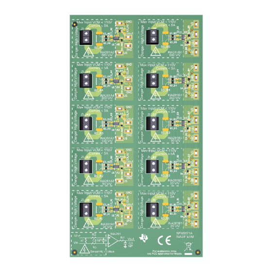
Item Item Part Number Quantity INA281EVM test board INA281EVM Related Documentation From Texas Instruments This document provides information regarding Texas Instruments' integrated circuits used in the assembly of the INA281EVM. Table 3. Related Documentation Document Literature Number INA281 product data sheet... - Page 5 (EMC) testing. The INA281EVM consists of one PCB with an option to cut out ten individual PCBs, one for each of the five gain options (1 to 5) and the two different pin outs (A and B) listed in Table 1.
-
Page 6: Operation
Operation Quick Start Setup Follow these procedures to set up and use one of the panels of the INA281EVM. For the following instructions, X is pinout A or B, and n is gain option 1, 2, 3, 4, or 5. - Page 7 EVM Components www.ti.com EVM Components This section summarizes the INA281EVM components. For the following instructions, X is pinout A or B, and n is gain option 1, 2, 3, 4, or 5. R2_Xn, R3_Xn, R4_Xn, C2_Xn, C3_Xn R2_Xn, R3_Xn, R4_Xn, are factory-installed 0-Ω 0603 resistors.
- Page 8 INA281EVM PCBs. Schematics Figure 1 shows the schematic of the INA281EVM for all gain versions for the A pinout. The difference is noted on the reference designator ending in the gain option _An. Figure 2 shows the B1 gain panel and this is also a copy for all the other gain options with the reference designator ending with the gain option _Bn.
- Page 9 Schematic, PCB Layout, and Bill of Materials www.ti.com Figure 2. INA281EVM Schematic: Gain B1 Panel SBOU244 – June 2020 INA281EVM Submit Documentation Feedback Copyright © 2020, Texas Instruments Incorporated...
-
Page 10: Pcb Layout
Schematic, PCB Layout, and Bill of Materials www.ti.com PCB Layout Figure 3 through Figure 9 illustrate the PCB layout for the INA281EVM. Figure 3. INA281EVM Top Overlay Figure 4. INA281EVM Bottom Overlay INA281EVM SBOU244 – June 2020 Submit Documentation Feedback... - Page 11 Schematic, PCB Layout, and Bill of Materials www.ti.com Figure 5. INA281EVM Top Layer Figure 6. INA281EVM Bottom Layer SBOU244 – June 2020 INA281EVM Submit Documentation Feedback Copyright © 2020, Texas Instruments Incorporated...
- Page 12 Schematic, PCB Layout, and Bill of Materials www.ti.com Figure 7. INA281EVM Top Solder Figure 8. INA281EVM Bottom Solder INA281EVM SBOU244 – June 2020 Submit Documentation Feedback Copyright © 2020, Texas Instruments Incorporated...
- Page 13 Schematic, PCB Layout, and Bill of Materials www.ti.com Figure 9. INA281EVM Drill Drawing SBOU244 – June 2020 INA281EVM Submit Documentation Feedback Copyright © 2020, Texas Instruments Incorporated...
- Page 14 Schematic, PCB Layout, and Bill of Materials www.ti.com Bill of Materials Table 4 provides the parts list for the INA281EVM. Table 4. Bill of Materials Designator Value Description Package Reference Part Number Manufacturer C1_A1, C1_A2, C1_A3, C1_A4, 0.1uF CAP, CERM, 0.1 uF, 25 V, +/- 10%, X7R, AEC-Q200 Grade 1,...
- Page 15 Fiducial mark. There is nothing to buy or mount. R1_A1, R1_A2, R1_A3, R1_A4, 0.01 RES, 0.01, 1%, 3 W, 2512 2512 CRA2512-FZ-R010ELF Bourns R1_A5, R1_B1, R1_B2, R1_B3, R1_B4, R1_B5 SBOU244 – June 2020 INA281EVM Submit Documentation Feedback Copyright © 2020, Texas Instruments Incorporated...
- Page 16 TI products. TI’s provision of these resources does not expand or otherwise alter TI’s applicable warranties or warranty disclaimers for TI products. Mailing Address: Texas Instruments, Post Office Box 655303, Dallas, Texas 75265 Copyright © 2020, Texas Instruments Incorporated...
Need help?
Do you have a question about the INA281EVM and is the answer not in the manual?
Questions and answers