Table of Contents
Advertisement
Quick Links
www.ti.com
User's Guide
INA233EVM Rev A User's Guide And Software Tutorial
This EVM user's guide describes the characteristics, operation, and use of the INA233EVM evaluation board. It
discusses how to set up and configure the software and hardware, and reviews various aspects of the program
operation. Throughout this document, the terms evaluation board, evaluation module, and EVM are synonymous
with the INA233EVM. This EVM user's guide also includes information regarding operating procedures and
input/output connections, an electrical schematic, printed circuit board (PCB) layout drawings, and a parts list for
the EVM.
SBOU187A – APRIL 2017 – REVISED APRIL 2023
Submit Document Feedback
ABSTRACT
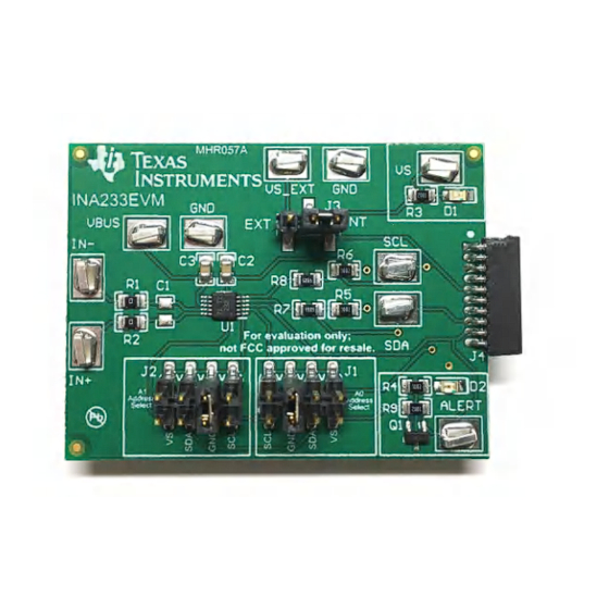
Figure 1-1. INA233EVM Evaluation Module
Copyright © 2023 Texas Instruments Incorporated
INA233EVM Rev A User's Guide And Software Tutorial
1
Advertisement
Table of Contents

Subscribe to Our Youtube Channel
Related Manuals for Texas Instruments INA233EVM


Summary of Contents for Texas Instruments INA233EVM
-
Page 1: Figure 1-1. Ina233Evm Evaluation Module
INA233EVM Rev A User's Guide And Software Tutorial ABSTRACT This EVM user's guide describes the characteristics, operation, and use of the INA233EVM evaluation board. It discusses how to set up and configure the software and hardware, and reviews various aspects of the program operation. -
Page 2: Table Of Contents
Figure 3-3. Connecting the INA233 Test Board and SM-USB-DIG Platform Board to the Computer........Figure 3-4. Connecting the INA233 Test Board and SM-USB-DIG Platform Board..............11 Figure 3-5. INA233 Power Up Using SM_USB DIG and INA233EVM GUI Software..............12 Figure 3-6. VDUT Voltage Selection in INA233EVM GUI......................12... - Page 3 Layer..........................27 List of Tables Table 1-1. INA233EVM Kit Contents............................4 Table 1-2. Related Documentation.............................. Table 2-1. Signal Definition of J4 on INA233EVM Board......................7 Table 3-1. INA233EVM Test Board Jumper Functions......................Table 4-1. INA233 I C Address Configuration........................... Table 5-1. Bill of Materials: INA233EVM............................28...
-
Page 4: Overview
Programmable calibration value, conversion times, and averaging, combined with an internal multiplier, enable direct readouts of current in amperes and power in watts. The INA233EVM is a platform for evaluating the performance of the INA233 under various signal, shunt, and supply conditions. -
Page 5: Related Documentation From Texas Instruments
The following documents provide information regarding Texas Instruments integrated circuits used in the assembly of the INA233EVM. This EVM user's guide is available from the TI web site under literature number SBOU187. Any letter appended to the literature number corresponds to the document revision that is current at the time of the writing of this document. -
Page 6: Theory Of Operation For Ina233 Hardware
INA233EVM Hardware www.ti.com 2.1 Theory of Operation for INA233 Hardware Figure 2-2 depicts a block diagram of the INA233EVM PCB highlighting the power supplies, analog inputs, and digital I/O signals. VBUS Supply (DVDD) 10-Pin Female I C Address SM-USB-DIG INA233... -
Page 7: Signal Definitions Of H1 (10-Pin Connector Socket)
2.2 Signal Definitions of H1 (10-Pin Connector Socket) Table 2-1 lists the pinout for the 10-pin connector socket used to communicate between the INA233EVM and the SM-USB-DIG. It should be noted that the INA233EVM only uses the necessary I C communication lines (pins 1 and 3) and the VS and GND pins (pin 6 and pin 8) to issue commands to the INA233 chip. -
Page 8: Sm-Usb-Dig Platform Description
Figure 2-3 shows the block diagram for the SM-USB-DIG Platform. This platform is a general-purpose data acquisition system that is used on several different Texas Instruments evaluation modules. The details of its operation are included in a separate document, SBOU098 (available for download at www.ti.com). -
Page 9: Ina233Evm Hardware Setup
Windows 7 is the recommended operating system. 3.2.2 Software Installation Make sure the hardware is not connected to the computer. Download the INA233EVM GUI from the INA233 Tools & Software folder. Extract the contents of the downloaded .zip file and run Setup_INA233EVM.exe. Follow... -
Page 10: Configuration Of Ina233Evm Jumper Settings
Figure 3-2. INA233EVM Default Jumper Settings Typically, jumper 3 (J3) on the INA233EVM is always set to the INT position. When set to the INT position, the SM-USB-DIG Platform provides the supply for the INA233. When this jumper is set to the EXT position, an external supply voltage can be connected to test point VS_EXT to provide the supply for the INA233. -
Page 11: Connecting The Hardware
3.4 Connecting the Hardware To set up the INA233EVM and connect the two PCBs of the EVM together (that is, the INA233 test board and SM-USB-DIG Platform board), gently slide the male and female ends of the 10-pin connectors together. -
Page 12: System Power Up
3.4.1 System Power Up Launch the INA233EVM GUI software. By default the Power button on the GUI is enabled so the VS LED on the EVM (D1) immediately lights up, indicating that the EVM PCB is receiving power, as shown Figure 3-5. -
Page 13: Ina233Evm Features
3.5.5 IN+/IN– Input Filter (R1, R2, and C1) The INA233EVM has an optional input filter to remove high-frequency noise from the inputs IN+ and IN–. This filter is typically unpopulated. The default values for R1 and R2 are 0-Ω resistors. -
Page 14: Shunt Monitor Configuration
Depending on the user’s needs, either of these configurations can be used without making any changes to the INA233EVM board or software. The INA233EVM have VBUS, GND, IN+ and IN- test points. Use these test points to apply external voltage sources depending the configuration selected. -
Page 15: Ina233Evm Software Overview
INA233EVM Software Overview 4 INA233EVM Software Overview This section discusses how to use the INA233EVM software. Software operation involves a two-step process: configuration of the INA233 settings, and operation of the tool. 4.1 Starting the INA233EVM Software The INA233 software can be operated through the Windows Start menu. From Start, select All Programs; then select the INA233EVM program. -
Page 16: Configuring The Ina233Evm Software
Figure 4-2. INA233EVM Software: Communication Error With the SM-USB-DIG Platform 4.2 Configuring the INA233EVM Software The INA233EVM software first requires a series of setup processes to configure the device and make sure that the software works properly. 1. Set I C Address on the SM-USB-DIG Tab 2. -
Page 17: C Address Selection
Figure 4-3. Setting the I C Address SBOU187A – APRIL 2017 – REVISED APRIL 2023 INA233EVM Rev A User's Guide And Software Tutorial Submit Document Feedback Copyright © 2023 Texas Instruments Incorporated... -
Page 18: Set The Configuration Register (Mfr_Adc_Config)
Setting the conversion times allows the user to customize the amount of measurement time for conversions. Typically, for the INA233EVM software, the user is not able to notice a visual difference between the conversion times unless a high averaging mode and conversion time are chosen. The Shunt and Bus conversion times can... -
Page 19: Set Calibration Register (Mfr_Calibration)
The Device Configuration tab of the INA233EVM GUI allows the user to set the averaging mode (AVG[2:0]), Vbus conversion time (VBUSCT[2:0]), Vshunt conversion time(VSHCT[2:0]) and operating mode (MODE[2:0]). -
Page 20: Register
4-10. Refer to data sheet Standard PMBus Commands section for register descriptions. Figure 4-10. Set the Warning Limit Registers INA233EVM Rev A User's Guide And Software Tutorial SBOU187A – APRIL 2017 – REVISED APRIL 2023 Submit Document Feedback Copyright © 2023 Texas Instruments Incorporated... -
Page 21: Using The Ina233Evm Software
INA233EVM Software Overview 4.3 Using the INA233EVM Software After configuring the INA233EVM software, the rest of the tabs can be evaluated. This section describes the basic operation of the device, and offers guidelines for interpreting the graphic user interface (GUI). -
Page 22: Status Register Tab
STATUS_CML (0x7Eh): Retrieves information about communications status. • STATUS_MFR_SPECIFIC (0x80h): Retrieves information about manufacturer-specific device status. Figure 4-12. Status Register Tab INA233EVM Rev A User's Guide And Software Tutorial SBOU187A – APRIL 2017 – REVISED APRIL 2023 Submit Document Feedback Copyright © 2023 Texas Instruments Incorporated... -
Page 23: Register Map Tab
The Register tab contains information on the individual operation of the INA233 registers as shown in Figure 4-13. Figure 4-13. Registers Map Tab SBOU187A – APRIL 2017 – REVISED APRIL 2023 INA233EVM Rev A User's Guide And Software Tutorial Submit Document Feedback Copyright © 2023 Texas Instruments Incorporated... -
Page 24: Plots Tab
Capture Data in Loop button above the plot to begin polling for data. Figure 4-14. Graphing the INA233 Data INA233EVM Rev A User's Guide And Software Tutorial SBOU187A – APRIL 2017 – REVISED APRIL 2023 Submit Document Feedback Copyright ©... -
Page 25: Ina233Evm Documentation
INA233EVM Documentation 5 INA233EVM Documentation This section contains the complete bill of materials, schematic diagram, and PCB layout for the INA233EVM. Note The board layout is not to scale. This image is intended to show how the board is laid out; it is not intended to be used for manufacturing INA233EVM PCBs. -
Page 26: Pcb Layout
PCB layout for the INA233EVM. Figure 5-2. INA233EVM PCB Top Overlay Figure 5-3. INA233EVM PCB Top Solder INA233EVM Rev A User's Guide And Software Tutorial SBOU187A – APRIL 2017 – REVISED APRIL 2023 Submit Document Feedback Copyright © 2023 Texas Instruments Incorporated... -
Page 27: Figure 5-4. Ina233Evm Pcb Top Layer
INA233EVM Documentation Figure 5-4. INA233EVM PCB Top Layer Figure 5-5. INA233EVM PCB Bottom Layer SBOU187A – APRIL 2017 – REVISED APRIL 2023 INA233EVM Rev A User's Guide And Software Tutorial Submit Document Feedback Copyright © 2023 Texas Instruments Incorporated... -
Page 28: Bill Of Materials
INA233EVM Documentation www.ti.com 5.3 Bill of Materials Table 5-1 lists the bill of materials for the INA233EVM. Table 5-1. Bill of Materials: INA233EVM DESIGNATOR QUANTITY VALUE DESCRIPTION PACKAGE REFERENCE PART NUMBER MANUFACTURER !PCB Printed Circuit MHR057 Board C2, C3 0.1 µF CAP, CERM, 0.1... -
Page 29: Revision History
• Changed document title to include software tutorial content................• Added registered trademark for Windows®......................9 SBOU187A – APRIL 2017 – REVISED APRIL 2023 INA233EVM Rev A User's Guide And Software Tutorial Submit Document Feedback Copyright © 2023 Texas Instruments Incorporated... - Page 30 STANDARD TERMS FOR EVALUATION MODULES Delivery: TI delivers TI evaluation boards, kits, or modules, including any accompanying demonstration software, components, and/or documentation which may be provided together or separately (collectively, an “EVM” or “EVMs”) to the User (“User”) in accordance with the terms set forth herein.
-
Page 31: Software
www.ti.com Regulatory Notices: 3.1 United States 3.1.1 Notice applicable to EVMs not FCC-Approved: FCC NOTICE: This kit is designed to allow product developers to evaluate electronic components, circuitry, or software associated with the kit to determine whether to incorporate such items in a finished product and software developers to write software applications for use with the end product. - Page 32 www.ti.com Concernant les EVMs avec antennes détachables Conformément à la réglementation d'Industrie Canada, le présent émetteur radio peut fonctionner avec une antenne d'un type et d'un gain maximal (ou inférieur) approuvé pour l'émetteur par Industrie Canada. Dans le but de réduire les risques de brouillage radioélectrique à...
- Page 33 www.ti.com EVM Use Restrictions and Warnings: 4.1 EVMS ARE NOT FOR USE IN FUNCTIONAL SAFETY AND/OR SAFETY CRITICAL EVALUATIONS, INCLUDING BUT NOT LIMITED TO EVALUATIONS OF LIFE SUPPORT APPLICATIONS. 4.2 User must read and apply the user guide and other available documentation provided by TI regarding the EVM prior to handling or using the EVM, including without limitation any warning or restriction notices.
- Page 34 Notwithstanding the foregoing, any judgment may be enforced in any United States or foreign court, and TI may seek injunctive relief in any United States or foreign court. Mailing Address: Texas Instruments, Post Office Box 655303, Dallas, Texas 75265 Copyright © 2023, Texas Instruments Incorporated...
- Page 35 TI products. TI’s provision of these resources does not expand or otherwise alter TI’s applicable warranties or warranty disclaimers for TI products. TI objects to and rejects any additional or different terms you may have proposed. IMPORTANT NOTICE Mailing Address: Texas Instruments, Post Office Box 655303, Dallas, Texas 75265 Copyright © 2023, Texas Instruments Incorporated...
Need help?
Do you have a question about the INA233EVM and is the answer not in the manual?
Questions and answers