
Related Manuals for CIS VCC-12CL1M


Summary of Contents for CIS VCC-12CL1M
- Page 1 VCC-12CL1M Rev. 900-795-35-00 English Camera Link I/F 12M Pixels CMOS B/W Camera VCC-12CL1M Product Specifications & Operational Manual CIS Corporation ©2016 CIS Corporation. All rights reserved.
-
Page 2: Table Of Contents
Remote Communication Function .......................... 22 Factory Settings ..............................23 CMOS Optical Axis Accuracy ..........................24 Dimensions ................................. 25 Cases for Indemnity (Limited Warranty) ........................ 29 CMOS Pixel Defect ............................... 29 Product Support ..............................29 Ordering Information ............................30 ©2016 CIS Corporation. All rights reserved. -
Page 3: Scope Of Application
VCC-12CL1M Rev. 900-795-35-00 Scope of Application This is to describe VCC-12CL1M, 12M resolution, Camera Link B/W CMOS Camera. All specifications contained herein are subject to change without prior notice. Reproduction in whole or in part is prohibited. 2. Handling Precautions The camera must not be used for any nuclear equipments or aerospace equipments with which mechanical failure or malfunction could result in serious bodily injury or loss of human life. -
Page 4: Product Outline
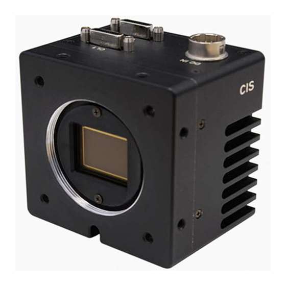
Voltage Rising Time [ ms ] Product Outline VCC-12CL1M is a Camera Link interfaced and 12M resolution industrial B/W video camera module. 12M pixels CMOS sensor with diagonal length 23.5mm4/3 is utilized. Entire pixels can be read out within 1/43s at Full Configuration output. -
Page 5: Cautions
Fixed Shutter Trigger Mode/ Pulse Width Shutter Trigger Mode (19) Partial Scan Full frame scan ~2 lines(2 lines/step) (20) Safety/Quality standards UL: Conform to UL Standard including materials and others. EN55022:2010(ClassA) for Emission EN61000-6-2:2005 for Immunity RoHS: Conform to RoHS. ©2016 CIS Corporation. All rights reserved. -
Page 6: Camera Output Signal Specification
※ 3 seconds shall be waited after turning on power to get proper camera operation. +5.0V( VCC) 100Ω FVAL Output LVAL Output DVAL Output HD74LV1GT32 ACME(RENESAS) Exposure Output Voh:3.8V(Min) Vol:0.55V( Max) 100Ω Trigger Input ©2016 CIS Corporation. All rights reserved. HD74LV1GT14 ACME(RENESAS) Vt-:0.5(Min) Vt+:1.9V(Max) -
Page 7: Spectral Sensitivity Characteristic
※the lens characteristic and the illuminant characteristic are excluded. Video Output Format (1) Medium Configuration Mode : 22fps 4000 Pixel ・・・ (2) Full , 8Tap10Bit Configuration Mode : 43fps (Factory settings) 4000 Pixel ・・・ ©2016 CIS Corporation. All rights reserved. -
Page 8: Function Settings
1/25000s 1/35000s 1/70000s 1/40000s 1/35000s 1/70000s 1/85000s Fixed Trigger Shutter Mode Medium Full , 8Tap10Bit 10Tap Configuration Configuration Configuration Mode Mode Mode 1/22s(OFF) 1/43s(OFF) 1/54s(OFF) 1/60s 1/60s 1/60s 1/100s 1/100s 1/100s 1/120s 1/120s 1/120s ©2016 CIS Corporation. All rights reserved. - Page 9 12bit output (12bit cannot be output at 8Tap/10Tap mode) Reflection partial scan 1: Check a setting error of each partial scan area and execute the partial setting value scan without error. Partial Scan Mode Full Frame Scan Mode Partial Scan Mode ©2016 CIS Corporation. All rights reserved.
- Page 10 ※Set the data of Address 15 to 1. ※Odd setting is not acceptable 9600bps (factory-configurable) Baud rate 115200bps (factory-configurable) Factory Settings Input 68 to set back to factory settings. Data Save Input 83 to save the data to EEP-ROM. ©2016 CIS Corporation. All rights reserved.
-
Page 11: External Connector Pin Assignment
VCC-12CL1M Rev. 900-795-35-00 External Connector Pin Assignment 12 pins Circular Connector HR10-10R-12PA (HIROSE) equivalent 7.1. Pin No. Power Input (DC+12V) LVAL Output FVAL Output EXPOSURE Output DVAL Output Trigger Input ©2016 CIS Corporation. All rights reserved. -
Page 12: Camera Link Connector 12226-1100-00Pl (Sumitomo 3M)
When changing the selection of the switch, please confirm that the power of the power supply source is turned OFF always. Changing the switch at the powering up might cause malfunction to the camera. ©2016 CIS Corporation. All rights reserved. -
Page 13: Timing Chart
← Approx.156H at Binarization Mode (Output image is delayed by 2H) Exposure Time(*1) SP Out(Exposure Out) 1H = 14.028us *1 Exposure Time : (Address9) Min 28.1us ~ Max 42.1ms 4Tap Medium Configuration Output 22.6fps モード ©2016 CIS Corporation. All rights reserved. -
Page 14: Horizontal Synchronous Signals Timing (Full , 8Tap10Bit Configuration Mode : 43Fps)
←Approx.156H at Binarization Mode (Output image is delayed by 2H) SP Out(Exposure Out) Exposure Time (*1) 1H = 7.222us *1 Exposure Time : (Address9) Min 14.4us ~ Max 21.7ms 8Tap Full Configuration Output 43.9fps モード ©2016 CIS Corporation. All rights reserved. -
Page 15: Horizontal Synchronous Signals Timing (10Tap Configuration Mode : 54Fps)
About ←Approx.156H at Binarization Mode (Output image is delayed by 2H) Exposure Out(12P) Exposure Time (*1) 1H = 5.778us *1 Exposure Time : (Address9) Min 11.6us ~ Max 17.3ms 10Tap Configuration Output 54.8fps モード ©2016 CIS Corporation. All rights reserved. -
Page 16: Fixed Trigger Shutter Mode
Effective Line : 3000H (Trigger input ignore period) TRIG IN ① ② SP Out (Exposure Out) Medium Configuration Mode ①max 170us ②max 30us Full Configuration Mode ①max 90us ②max 17us 10Tap Configuration Mode ①max 72us ②max 14us ©2016 CIS Corporation. All rights reserved. -
Page 17: Pulse Width Trigger Shutter Mode
Effective Line : 3000H (Trigger input ignore period) TRIG IN ① ② SP Out (Exposure Out) Medium Configuration Mode ①max 170us ②max 30us Full Configuration Mode ①max 90us ②max 17us 10Tap Configuration Mode ①max 72us ②max 14us ©2016 CIS Corporation. All rights reserved. -
Page 18: Binarization
Not effective when there is only horizontal edge. ※ Set a parameter of binarization threshold value to 512d. ※ Manual ・・・ Based on a parameter of binarization threshold value, the binarization is performed. ©2016 CIS Corporation. All rights reserved. -
Page 19: Shading Correction
When the object with uniform levels, such as a pattern box, is imaged on the whole screen and a shading correction data calculation start (address 27) is set ON, the correction data is calculated inside a camera automatically and saved. Start the shading correction data setting at full frame scan mode. ©2016 CIS Corporation. All rights reserved. -
Page 20: Partial Scan Mode
Example : 3 partial areas to be set. ① : V Blanking (Fixed to 156H) ② : Partial Area 1 ③ : Partial Area 2 ④ : Partial Area 3 ⑤ : Total line count per frame ©2016 CIS Corporation. All rights reserved. - Page 21 □ The line numbers at partial scan setting can be set from 2 lines. □ At partial scan setting, the gain(AGC) and the shutter(AE) turn to be OFF □ The effective line numbers of the manual shutter setting value at partial scan setting become the maximum. ©2016 CIS Corporation. All rights reserved.
-
Page 22: Remote Communication Function
(4) 【Example for Get Command】 To get the information of the address 33 [Send] GU[sp]33[¥r] or[¥n] [¥r]=CR(0x0D) [Returned value] 50[¥r] [¥n] [Acquired data + Linefeed] [¥n]=LF(0x0A) [Returned value] [¥r] [¥n] [Linefeed] [sp]=Space(0x20) [Returned value] >[sp] [Prompt + Space] ©2016 CIS Corporation. All rights reserved. -
Page 23: Factory Settings
Full Frame Scan Mode Vertical Flip Horizontal Flip Gamma Correction Binarization Shading Correction Defective Pixel Correction Camera Mode Full Configuration Mode Factory setting of the Switch at the back Power Supply Selection (PoCL) CL side ©2016 CIS Corporation. All rights reserved. -
Page 24: Cmos Optical Axis Accuracy
VCC-12CL1M Rev. 900-795-35-00 CMOS Optical Axis Accuracy ©2016 CIS Corporation. All rights reserved. -
Page 25: Dimensions
VCC-12CL1M Rev. 900-795-35-00 Dimensions ©2016 CIS Corporation. All rights reserved. - Page 26 VCC-12CL1M Rev. 900-795-35-00 ©2016 CIS Corporation. All rights reserved.
- Page 27 VCC-12CL1M Rev. 900-795-35-00 ©2016 CIS Corporation. All rights reserved.
- Page 28 VCC-12CL1M Rev. 900-795-35-00 ©2016 CIS Corporation. All rights reserved.
-
Page 29: Cases For Indemnity (Limited Warranty)
On very rare occasions, however, CMOS pixel defects might be noted with time of usage of the products. Cause of the CMOS pixel defects is the characteristic phenomenon of CMOS itself and CIS is exempted from taking any responsibilities for them. Should you have any questions on CMOS pixel defects compensation, please contact us. -
Page 30: 19. Ordering Information
VCC-12CL1M Rev. 900-795-35-00 19. Ordering Information Connector Model Name Baud Rate(bps) Position VCC-12CL1M-T1 115200 VCC-12CL1M-T9 9600 VCC-12CL1M-B1 BOTTOM 115200 VCC-12CL1M-B9 BOTTOM 9600 VCC-12CL1M-L1 LEFT 115200 VCC-12CL1M-L9 LEFT 9600 VCC-12CL1M-R1 RIGHT 115200 VCC-12CL1M-R9 RIGHT 9600 ©2016 CIS Corporation. All rights reserved.
Need help?
Do you have a question about the VCC-12CL1M and is the answer not in the manual?
Questions and answers