
Related Manuals for Holtek HT66FM5340


Summary of Contents for Holtek HT66FM5340
- Page 1 Brushless DC MCU with Pre-driver HT66FM5340 Revision: V1.00 Date: December 07, 2018...
-
Page 2: Table Of Contents
HT66FM5340 Brushless DC MCU with Pre-driver Table of Contents Features ........................ 6 CPU Features ..........................6 Peripheral Features ........................6 General Description ..................... 7 Block Diagram ...................... 7 Pin Assignment ....................8 Pin Description ....................8 Absolute Maximum Ratings ................11 D.C. Characteristics ................... 11 Operating Voltage Characteristics ..................... - Page 3 HT66FM5340 Brushless DC MCU with Pre-driver Data Memory ...................... 24 Structure .............................24 Data Memory Addressing ......................25 General Purpose Data Memory ....................25 Special Purpose Data Memory ....................25 Special Function Register Description ............27 Indirect Addressing Registers – IAR0, IAR1, IAR2 ..............27 Memory Pointers –...
- Page 4 HT66FM5340 Brushless DC MCU with Pre-driver TM External Pins ........................56 Programming Considerations .....................56 Periodic Type TM – PTM ..................58 Periodic TM Operation ......................59 Periodic Type TM Register Description ..................60 Periodic Type TM Operating Modes ..................67 Capture Timer Module – CAPTM ..............81 Capture Timer Overview ......................81...
- Page 5 HT66FM5340 Brushless DC MCU with Pre-driver Interrupts ......................133 Interrupt Registers ........................133 Interrupt Operation ........................141 Hall Sensor Interrupts ......................142 External Interrupt 1 ........................143 Noise Filter Input Interrupt ......................143 Comparator 0 Interrupt ......................144 Capture Timer Module Interrupts .....................144 Multi-function Interrupts ......................144 PWM Module Interrupts ......................144...
-
Page 6: Features
HT66FM5340 Brushless DC MCU with Pre-driver Features CPU Features • Operating voltage =32kHz~20MHz: 4.5V~5.5V ♦ • Up to 0.2μs instruction cycle with 20MHz system clock at V • Power down and wake-up functions to reduce power consumption • Oscillator types Internal High Speed 20MHz RC –... -
Page 7: General Description
HT66FM5340 Brushless DC MCU with Pre-driver General Description The HT66FM5340 is a Flash Memory 8-bit high performance RISC architecture microcontroller, which includes a host of fully integrated special features specifically designed for brushless DC motor applications. The device includes an internal LDO (Low Dropout Regulator) for voltage regulation with a 12V input and 5V output as well as an internal pre-driver which provides a 12V high voltage output, which can directly drive a P-N MOSFET driver or a BLCD motor. -
Page 8: Pin Assignment
3. The OCDSDA and OCDSCK pins are supplied as dedicated OCDS pins and as such only available for the HT66VM5340 device which is the OCDS EV chip for the HT66FM5340 device. 4. For the less pin count package type there will be unbounded pins which should be properly configured to avoid unwanted power consumption resulting from floating input conditions. - Page 9 HT66FM5340 Brushless DC MCU with Pre-driver Pin Name Function Description PAPU General purpose I/O. Register enabled pull-up and PAWU CMOS wake-up PAPS0 PA3/H1/PTP1I/C1P PAPS0 — Hall sensor input PTP1I PAPS0 — PTM1 input PAPS0 — Comparator 1 positive input PAPU General purpose I/O.
- Page 10 HT66FM5340 Brushless DC MCU with Pre-driver Pin Name Function Description PBPU CMOS General purpose I/O. Register enabled pull-up PBPS0 PTCK0 PBPS0 — PTM0 clock input PTCK3 PBPS0 — PTM3 clock input PB2/PTCK0/PTCK3/ [NFIN]/AN1/HCO/PTP2 NFIN — External Noise Filter input PBPS0 PBPS0 —...
-
Page 11: Absolute Maximum Ratings
HT66FM5340 Brushless DC MCU with Pre-driver Absolute Maximum Ratings Supply Voltage (V ) ..................V -0.3V to 15V Supply Voltage (V ) ....................V -0.3V to 6.0V High Voltage Input Voltage ................V -0.3V to V +0.3V Input Voltage ..................... V -0.3V to V +0.3V... -
Page 12: Operating Current Characteristics
HT66FM5340 Brushless DC MCU with Pre-driver Operating Current Characteristics Ta=-40°C~85°C Test Conditions Symbol Parameter Min. Typ. Max. Unit Conditions Operating Current – HIRC 5V f =20MHz — HIRC Additional Current for HIRC Enable 5V f =20MHz — μA HIRC HIRC Note: When using the characteristic table data, the following notes should be taken into consideration: 1. -
Page 13: Operating Frequency Characteristic Curves
HT66FM5340 Brushless DC MCU with Pre-driver Operating Frequency Characteristic Curves System Operating Frequency 20MHz 4.5V 5.5V Operating Voltage System Start Up Time Characteristics Ta=-40°C~85°C Test Conditions Symbol Parameter Min. Typ. Max. Unit Conditions — f /64, f — — System Start-up Time... -
Page 14: Input/Output Characteristics
HT66FM5340 Brushless DC MCU with Pre-driver Input/Output Characteristics Ta=-40°C~85°C Test Conditions Symbol Parameter Min. Typ. Max. Unit Conditions Input Low Voltage for I/O Ports — — 0.3V Input High Voltage for I/O Ports — 0.7V — Sink Current for I/O Ports 5V V =0.1V... -
Page 15: Low Dropout Regulator Electrical Characteristics
HT66FM5340 Brushless DC MCU with Pre-driver Low Dropout Regulator Electrical Characteristics +1V, Ta=-40°C~85°C, unless otherwise specified =10μF+0.1μF LOAD Test Conditions Symbol Parameter Min. Typ. Max. Unit Conditions Input Voltage — — +0.1 Ta=25°C, — =1mA, V =5.0V Output Voltage LOAD —... -
Page 16: A/D Converter Electrical Characteristics
HT66FM5340 Brushless DC MCU with Pre-driver A/D Converter Electrical Characteristics Ta=-40°C~85°C Test Conditions Symbol Parameter Min. Typ. Max. Unit Conditions A/D Converter Operating Voltage — — Additional Current for A/D Converter Enable — — — A/D Converter Standby Current —... -
Page 17: Comparators Electrical Characteristics
HT66FM5340 Brushless DC MCU with Pre-driver Test Conditions Symbol Parameter Min. Typ. Max. Unit Conditions 3.3V +0.1 — -1.4 Gain=1, Ga<±5% +0.1 — -1.4 PGA Input Voltage Range 3.3V Gain=5, 10, 20 +0.1 — (Max)/Gain Ga<±5% +0.1 — (Max)/Gain 3.3V —... -
Page 18: Power-On Reset Characteristics
Time System Architecture A key factor in the high-performance features of the Holtek range of microcontrollers is attributed to their internal system architecture. The range of the device take advantage of the usual features found within RISC microcontrollers providing increased speed of operation and enhanced performance. -
Page 19: Program Counter - Pc
HT66FM5340 Brushless DC MCU with Pre-driver (System Clock) Phase Clock T1 Phase Clock T2 Phase Clock T3 Phase Clock T4 Program Counter PC+1 PC+2 Fetch Inst. (PC) Pipelining Execute Inst. (PC-1) Fetch Inst. (PC+1) Execute Inst. (PC) Fetch Inst. (PC+2) Execute Inst. -
Page 20: Stack
HT66FM5340 Brushless DC MCU with Pre-driver Stack This is a special part of the memory which is used to save the contents of the Program Counter only. For this device the stack has 8 levels and neither part of the data nor part of the program space, and is neither readable nor writeable. -
Page 21: Flash Program Memory
HT66FM5340 Brushless DC MCU with Pre-driver Flash Program Memory The Program Memory is the location where the user code or program is stored. For the device the Program Memory is Flash type, which means it can be programmed and re-programmed a large number of times, allowing the user the convenience of code modification on the same device. - Page 22 HT66FM5340 Brushless DC MCU with Pre-driver The accompanying diagram illustrates the addressing data flow of the look-up table. Program Memory Last Page or TBHP Register Data 16 bits TBLP Register User Selected Register TBLH Register High Byte Low Byte Table Program Example The following example shows how the table pointer and table data is defined and retrieved from the microcontroller.
-
Page 23: In Circuit Programming - Icp
The provision of Flash type Program Memory provides the user with a means of convenient and easy upgrades and modifications to their programs on the same device. As an additional convenience, Holtek has provided a means of programming the microcontroller in- circuit using a 4-pin interface. This provides manufacturers with the possibility of manufacturing their circuit boards complete with a programmed or un-programmed microcontroller, and then programming or upgrading the program at a later stage. -
Page 24: On-Chip Debug Support - Ocds
Users can use the EV chip device to emulate the real chip device behavior by connecting the OCDSDA and OCDSCK pins to the Holtek HT-IDE development tools. The OCDSDA pin is the OCDS Data/Address input/output pin while the OCDSCK pin is the OCDS clock input pin. -
Page 25: Data Memory Addressing
HT66FM5340 Brushless DC MCU with Pre-driver Special Purpose Data Memory (Sector 0 & Sector 1) General Purpose Data Memory (Sector 0 & Sector 1) Sector 0 Sector 1 Data Memory Structure Data Memory Addressing For the device that supports the extended instructions, the desired Data Memory Sector is selected by the MP1H or MP2H register and the certain Data Memory address in the pointed sector is specified by the MP1L or MP2L register when using indirect addressing access. - Page 26 HT66FM5340 Brushless DC MCU with Pre-driver Sector 1 Sector 0 Sector 1 Sector 0 IAR0 IAR1 OCPS MP1L HDCR MP1H HDCD MPTC1 MPTC2 TBLP PTM1C0 TBLH PTM1C1 TBHP PTM1DL STATUS PTM1DH PTM1AL IAR2 PTM1AH MP2L PTM1RPL MP2H PTM1RPH PTM0C0 SMOD...
-
Page 27: Special Function Register Description
HT66FM5340 Brushless DC MCU with Pre-driver Special Function Register Description Most of the Special Function Register details will be described in the relevant functional section; however several registers require a separate description in this section. Indirect Addressing Registers – IAR0, IAR1, IAR2 The Indirect Addressing Registers, IAR0, IAR1 and IAR2, although having their locations in normal RAM register space, do not actually physically exist as normal registers. -
Page 28: Accumulator - Acc
HT66FM5340 Brushless DC MCU with Pre-driver Indirect Addressing Program Example 2 data .section ´data´ adres1 db ? adres2 db ? adres3 db ? adres4 db ? block db ? code .section at 0 ´code´ org 00h start: mov a, 04h ;... -
Page 29: Program Counter Low Register - Pcl
HT66FM5340 Brushless DC MCU with Pre-driver Program Counter Low Register – PCL To provide additional program control functions, the low byte of the Program Counter is made accessible to programmers by locating it within the Special Purpose area of the Data Memory. By manipulating this register, direct jumps to other program locations are easily implemented. - Page 30 HT66FM5340 Brushless DC MCU with Pre-driver In addition, on entering an interrupt sequence or executing a subroutine call, the status register will not be pushed onto the stack automatically. If the contents of the status registers are important and if the subroutine can corrupt the status register, precautions must be taken to correctly save it.
-
Page 31: Oscillators
HT66FM5340 Brushless DC MCU with Pre-driver Oscillators Various oscillator options offer the user a wide range of functions according to their various application requirements. The flexible features of the oscillator functions ensure that the best optimisation can be achieved in terms of speed and power saving. Oscillator selections and operation are selected through relevant control registers. -
Page 32: Internal High Speed Rc Oscillator - Hirc
As Holtek has provided this device with both high and low speed clock sources and the means to switch between them dynamically, the user can optimise the operation of their microcontroller to achieve the best performance/power ratio. - Page 33 HT66FM5340 Brushless DC MCU with Pre-driver High Speed Oscillator 6-stage HIRC Prescaler HLCLK, CKS2~CKS0 bits LIRC Low Speed Oscillator Time Base TBCK Device Clock Configurations Note: When the system clock source f is switched to f from f , the high speed oscillator will be turned off to conserve the power.
-
Page 34: System Operation Modes
HT66FM5340 Brushless DC MCU with Pre-driver System Operation Modes There are five different modes of operation for the microcontroller, each one with its own special characteristics and which can be chosen according to the specific performance and power requirements of the application. There are two modes allowing normal operation of the microcontroller, the FAST Mode and SLOW Mode. -
Page 35: Control Registers
HT66FM5340 Brushless DC MCU with Pre-driver Control Registers The SMOD register and the FSYSON bit in the CTRL register are used to control the internal clocks within the device. • SMOD Register Name CKS2 CKS1 CKS0 — IDLEN HLCLK —... -
Page 36: Operating Mode Switching
HT66FM5340 Brushless DC MCU with Pre-driver • CTRL Register Name FSYSON — — — — LVRF — — — — — — — — “x”: unknown Bit 7 FSYSON: f on/off control in IDLE Mode 0: Disable 1: Enable This bit is used to control whether the system clock is switched on or not in the IDLE Mode. - Page 37 HT66FM5340 Brushless DC MCU with Pre-driver IDLE1 FAST HALT instruction executed CPU stop IDLEN=1 CPU run FSYSON=1 IDLE0 SLEEP HALT instruction executed HALT instruction executed CPU stop IDLEN=1 CPU stop FSYSON=0 IDLEN=0 SLOW WDT on CPU run FAST Mode to SLOW Mode Switching...
- Page 38 HT66FM5340 Brushless DC MCU with Pre-driver SLOW Mode to FAST Mode Switching In SLOW mode the system clock uses LIRC low speed system oscillator. To switch back to the FAST mode, where the high speed system oscillator is used, the HLCLK bit should be set to “1” or HLCLK bit is “0”...
-
Page 39: Standby Current Considerations
HT66FM5340 Brushless DC MCU with Pre-driver Entering the IDLE1 Mode There is only one way for the device to enter the IDLE1 Mode and that is to execute the “HALT” instruction in the application program with both the IDLEN bit in the SMOD register equal to “1”... -
Page 40: Watchdog Timer
HT66FM5340 Brushless DC MCU with Pre-driver Each pin on Port A can be setup using the PAWU register to permit a negative transition on the pin to wake-up the system. When a Port A pin wake-up occurs, the program will resume execution at the instruction following the “HALT”... -
Page 41: Watchdog Timer Operation
HT66FM5340 Brushless DC MCU with Pre-driver 110: 2 111: 2 These three bits determine the division ratio of the Watchdog Timer source clock, which in turn determines the timeout period. • CTRL Register Name FSYSON — — — — LVRF —... -
Page 42: Reset And Initialisation
HT66FM5340 Brushless DC MCU with Pre-driver The maximum time-out period is when the 2 division ratio is selected. As an example, with a 32kHz LIRC oscillator as its source clock, this will give a maximum watchdog period of around 8s... - Page 43 HT66FM5340 Brushless DC MCU with Pre-driver Low Voltage Reset – LVR The microcontroller contains a low voltage reset circuit in order to monitor the supply voltage of the device and provides an MCU reset should the value fall below a certain predefined level.
-
Page 44: Reset Initial Conditions
HT66FM5340 Brushless DC MCU with Pre-driver Bit 6~3 Unimplemented, read as “0” LVRF: LVR function reset flag Bit 2 0: Not occur 1: Occurred This bit is set to 1 when a specific Low Voltage Reset situation condition occurs. This bit can only be cleared to 0 by the application program. - Page 45 HT66FM5340 Brushless DC MCU with Pre-driver The following table indicates the way in which the various components of the microcontroller are affected after a power-on reset occurs. Item Condition after RESET Program Counter Reset to zero Interrupts All interrupts will be disabled...
- Page 46 HT66FM5340 Brushless DC MCU with Pre-driver WDT Time-out WDT Time-out Register Power On Reset (Normal Operation) (IDLE/SLEEP) HVRC - - - - - - 0 0 - - - - - - 0 0 - - - - - - u u...
- Page 47 HT66FM5340 Brushless DC MCU with Pre-driver WDT Time-out WDT Time-out Register Power On Reset (Normal Operation) (IDLE/SLEEP) PTM1C0 0 0 0 0 0 - - - 0 0 0 0 0 - - - u u u u u - - -...
- Page 48 HT66FM5340 Brushless DC MCU with Pre-driver WDT Time-out WDT Time-out Register Power On Reset (Normal Operation) (IDLE/SLEEP) MFI6 - - 0 0 - - 0 0 - - 0 0 - - 0 0 - - u u - - u u...
-
Page 49: Input/Output Ports
Brushless DC MCU with Pre-driver Input/Output Ports Holtek microcontrollers offer considerable flexibility on their I/O ports. With the input or output designation of every pin fully under user program control, pull-high selections for all ports and wake-up selections on certain pins, the user is provided with an I/O structure to meet the needs of a wide range of application possibilities. -
Page 50: Port A Wake-Up
HT66FM5340 Brushless DC MCU with Pre-driver Port A Wake-up The HALT instruction forces the microcontroller into the SLEEP or IDLE Mode which preserves power, a feature that is important for battery and other low-power applications. Various methods exist to wake-up the microcontroller, one of which is to change the logic condition on one of the Port A pins from high to low. - Page 51 HT66FM5340 Brushless DC MCU with Pre-driver Pin-shared Function Selection Registers The limited number of supplied pins in a package can impose restrictions on the amount of functions a certain device can contain. However by allowing the same pins to share several different functions and providing a means of function selection, a wide range of different functions can be incorporated into even relatively small package sizes.
- Page 52 HT66FM5340 Brushless DC MCU with Pre-driver NFINPS1~NFINPS0: NFIN input source pin selection Bit 3~2 00: PA7 01: PA6 10: PB2 11: PA7 Bit 1~0 Unimplemented, read as “0” • PAPS0 Register Name PAS07 PAS06 PAS05 PAS04 PAS03 PAS02 PAS01 PAS00...
- Page 53 HT66FM5340 Brushless DC MCU with Pre-driver PAS13~PAS12: PA5 Pin-Shared function selection Bit 3~2 00: PA5/H3/PTP3I 01: C3P 10: PTP2 11: PTP1 Bit 1~0 PAS11~PAS10: PA4 Pin-Shared function selection 00: PA4/H2/PTP2I 01: C2P 10: PTP1 11: PTP2 • PBPS0 Register Name...
-
Page 54: I/O Pin Structures
HT66FM5340 Brushless DC MCU with Pre-driver PBS11~PBS10: PB4 Pin-Shared function selection Bit 1~0 00: PB4 01: C2N 10: PTP0 11: PTP3 I/O Pin Structures The accompanying diagram illustrates the internal structure of the I/O logic function. As the exact logical construction of the I/O pin will differ from this drawing, it is supplied as a guide only to assist with the functional understanding of the I/O logic function. -
Page 55: Timer Modules - Tm
HT66FM5340 Brushless DC MCU with Pre-driver Timer Modules – TM One of the most fundamental functions in any microcontroller device is the ability to control and measure time. To implement time related functions each device includes several Timer Modules, abbreviated to the name TM. The TMs are multi-purpose timing units and serve to provide operations such as Timer/Counter, Input Capture, Compare Match Output and Single Pulse Output as well as being the functional unit for the generation of PWM signals. -
Page 56: Tm Interrupts
HT66FM5340 Brushless DC MCU with Pre-driver TM Interrupts The TMs each has two internal interrupts, the internal comparator A and comparator P, which generate a TM interrupt when a compare match condition occurs. When a TM interrupt is generated it can be used to clear the counter and also to change the state of the TM output pin. - Page 57 HT66FM5340 Brushless DC MCU with Pre-driver As the CCRA, CCRB and CCRP registers are implemented in the way shown in the following diagram and accessing these register pairs is carried out in a specific way as described above, it is recommended to use the “MOV” instruction to access the CCRA, CCRB and CCRP low byte registers, named PTMnAL, PTMnBL and PTMnRPL, using the following access procedures.
-
Page 58: Periodic Type Tm - Ptm
HT66FM5340 Brushless DC MCU with Pre-driver Periodic Type TM – PTM The Periodic Type TM contains five operating modes, which are Compare Match Output, Timer/ Event Counter, Capture Input, Single Pulse Output and PWM Output modes. The Periodic TM can be controlled with two external input pins and can drive one external output pin. -
Page 59: Periodic Tm Operation
HT66FM5340 Brushless DC MCU with Pre-driver CCRP Comparator P Match 16-bit Comparator P PTnMPF Interrupt PTnOC b0~b15 Output Polarity Counter Clear 16-bit Count-up Counter PTPn Control Control PTnON PTnCCLR PTnPAU b0~b15 PTnPOL PTnM1, PTnM0 PTnCK PTnIO1, PTnIO0 Comparator A Match... -
Page 60: Periodic Type Tm Register Description
HT66FM5340 Brushless DC MCU with Pre-driver Periodic Type TM Register Description Overall operation of the Periodic Type TM is controlled using a series of registers. A read only register pair exists to store the internal counter 10-bit or 16-bit value, while two read/write register pairs exist to store the internal 10-bit or 16-bit CCRA value and CCRP value. - Page 61 HT66FM5340 Brushless DC MCU with Pre-driver PTnCK2~PTnCK0: Select PTMn Counter clock Bit 6~4 000: f 001: f 010: f 011: f 100: f 101: f 110: PTCKn rising edge clock 111: PTCKn falling edge clock These three bits are used to select the clock source for the PTMn. The external pin clock source can be chosen to be active on the rising or falling edge.
- Page 62 HT66FM5340 Brushless DC MCU with Pre-driver Capture Input Mode PTnTCLR[1:0]=00B: 00: Input capture at rising edge of input signal and the counter value will be latched into CCRA 01: Input capture at falling edge of input signal and the counter value will be...
- Page 63 HT66FM5340 Brushless DC MCU with Pre-driver PTnPOL: PTMn Output polarity control Bit 2 0: Non-invert 1: Invert This bit controls the polarity of the output pins. When the bit is set high the PTMn output pin will be inverted and not inverted when the bit is zero. It has no effect if the PTMn is in the Timer/Counter Mode.
- Page 64 HT66FM5340 Brushless DC MCU with Pre-driver Timer/Counter Mode Unused These two bits are used to determine how the PTMn operates when a certain condition is reached. The function that these bits select depends upon in which mode the PTMn is running.
- Page 65 HT66FM5340 Brushless DC MCU with Pre-driver When the bit is low, the counter will be cleared when a compare match occurs from the Comparator P or with a counter overflow. A counter overflow clearing method can only be implemented if the CCRP bits are all cleared to zero. The PTnCCLR bit is not used in the PWM Output Mode, Single Pulse Output Mode or Capture Input Mode.
- Page 66 HT66FM5340 Brushless DC MCU with Pre-driver • PTMnDH Register (n=0~1) Name Bit 7~0 D15~D8: PTMn Counter High Byte Register bit 7 ~ bit 0 PTMn 16-bit Counter bit 15 ~ bit 8 • PTMnDH Register (n=2~3) Name — — —...
-
Page 67: Periodic Type Tm Operating Modes
HT66FM5340 Brushless DC MCU with Pre-driver • PTMnRPL Register (n=0~3) Name Bit 7~0 D7~D0: PTMn CCRP Low Byte Register bit 7 ~ bit 0 PTMn 10-bit/16-bit CCRP bit 7 ~ bit 0 • PTMnRPH Register (n=0~1) Name Bit 7~0 D15~D8: PTMn CCRP High Byte Register bit 7 ~ bit 0 PTMn 16-bit CCRP bit 15 ~ bit 8 •... - Page 68 HT66FM5340 Brushless DC MCU with Pre-driver As the name of the mode suggests, after a comparison is matched, the PTMn output pin will change state. The PTMn output pin condition however only changes state when a PTMnAF interrupt request flag is generated after a compare match occurs from Comparator A. The PTMnPF interrupt request flag, generated from a compare match occurs from Comparator P, will have no effect on the PTMn output pin.
- Page 69 HT66FM5340 Brushless DC MCU with Pre-driver Counter Value PTnCCLR = 1; PTnM [1:0] = 00 CCRA = 0 CCRA > 0 Counter cleared by CCRA value Counter overflow 0x3FF/ 0xFFFF CCRA=0 Resume CCRA Pause Stop Counter Restart CCRP Time PTnON...
- Page 70 HT66FM5340 Brushless DC MCU with Pre-driver Timer/Counter Mode To select this mode, bits PTnM1 and PTnM0 in the PTMnC1 register should be set to 11 respectively. The Timer/Counter Mode operates in an identical way to the Compare Match Output Mode generating the same interrupt flags. The exception is that in the Timer/Counter Mode the PTMn output pin is not used.
- Page 71 HT66FM5340 Brushless DC MCU with Pre-driver Counter Value PTnM [1:0] = 10 Counter cleared by CCRP Counter Reset when PTnON returns high CCRP Counter Stop if Pause Resume PTnON bit low CCRA Time PTnON PTnPAU PTnPOL CCRA Int. Flag PTMnAF CCRP Int.
- Page 72 HT66FM5340 Brushless DC MCU with Pre-driver Single Pulse Output Mode To select this mode, bits PTnM1 and PTnM0 in the PTMnC1 register should be set to 10 respectively and also the PTnIO1 and PTnIO0 bits should be set to 11 respectively. The Single Pulse Output Mode, as the name suggests, will generate a single shot pulse on the PTMn output pin.
- Page 73 HT66FM5340 Brushless DC MCU with Pre-driver Counter Value PTnM [1:0] = 10 ; PTnIO [1:0] = 11 Counter stopped by CCRA Counter Reset when PTnON returns high CCRA Counter Stops by Resume Pause software CCRP Time PTnON Auto. set by...
- Page 74 HT66FM5340 Brushless DC MCU with Pre-driver Capture Input Mode (PTM0) To select this mode bits PTnM1 and PTnM0 in the PTMnC1 register should be set to 01 respectively. This mode enables external signals to capture and store the present value of the internal counter and can therefore be used for applications such as pulse width measurements.
- Page 75 HT66FM5340 Brushless DC MCU with Pre-driver Counter Value PTnM[1:0] = 01; PTnTCLR[1:0] = 00 Counter cleared by CCRP Counter Counter Stop Reset CCRP Resume Pause Time PTnON PTnPAU Active Active Active edge edge edge PTMn Capture Input Source CCRA Int.
- Page 76 HT66FM5340 Brushless DC MCU with Pre-driver PTnM[1:0] = 01; PTnTCLR[1:0] = 01 Counter Value Counter cleared by CCRP Counter Counter Stop Reset CCRP Resume Pause Time PTnON PTnPAU Active Active edge Active edge Active edge edge PTMn Capture Input Source CCRA Int.
- Page 77 HT66FM5340 Brushless DC MCU with Pre-driver PTnM[1:0] = 01; PTnTCLR[1:0] = 10 Counter cleared by Counter Value CCRP Counter Counter Stop Reset CCRP Resume Pause Time PTnON PTnPAU Active Active Active edge edge edge PTMn Capture Input Source CCRA Int.
- Page 78 HT66FM5340 Brushless DC MCU with Pre-driver PTnM[1:0] = 01; PTnTCLR[1:0] = 11 Counter Value Counter cleared by CCRP Counter Counter Reset Stop CCRP Resume Pause Time PTnON PTnPAU Active Active Active Active edge edge edge edge PTMn Capture Input Source CCRA Int.
- Page 79 HT66FM5340 Brushless DC MCU with Pre-driver Capture Input Mode (PTM1~PTM3) To select this mode bits PTnM1 and PTnM0 in the PTMnC1 register should be set to 01 respectively. This mode enables external signals to capture and store the present value of the internal counter and can therefore be used for applications such as pulse width measurements.
- Page 80 HT66FM5340 Brushless DC MCU with Pre-driver Counter Value PTnM[1:0] = 01 Counter cleared by CCRP Counter Counter Stop Reset CCRP Resume Pause Time PTnON PTnPAU Active Active Active edge edge edge PTMn Capture Pin PTPnI or PTCKn CCRA Int. Flag PTMnAF CCRP Int.
-
Page 81: Capture Timer Module - Captm
HT66FM5340 Brushless DC MCU with Pre-driver Capture Timer Module – CAPTM The Capture Timer Module is a timing unit specifically used for Motor Control purposes. The CAPTM is controlled by a programmable clock source. Capture Timer Overview At the core of the Capture Timer Module is a 16-bit count-up counter which is driven by a user selectable internal clock source which is some multiple of the system clock or by the PWMO. - Page 82 HT66FM5340 Brushless DC MCU with Pre-driver • CAPTC0 Register Name CAPTPAU CAPTCK2 CAPTCK1 CAPTCK0 CAPTON — CAPS1 CAPS0 — — Bit 7 CAPTPAU: CAPTM Counter Pause control 0: Run 1: Pause The counter can be paused by setting this bit high. Clearing the bit to zero restores normal counter operation.
- Page 83 HT66FM5340 Brushless DC MCU with Pre-driver CAPNFT: CAPTM Noise Filter sampling times definition Bit 4 0: 2 times 1: 4 times The CAPTM Noise Filter circuit requires sampling the signal twice or 4 times continuously, when the sampled signals are all the same, the signal will be acknowledged.
-
Page 84: Capture Timer Operation
HT66FM5340 Brushless DC MCU with Pre-driver • CAPTMAH Register Name Bit 7~0 D15~D8: CAPTM Compare High Byte Register bit 7 ~ bit 0 CAPTM 16-bit Compare Register bit 15 ~ bit 8 • CAPTMCL Register Name “x”: unknown Bit 7~0... - Page 85 HT66FM5340 Brushless DC MCU with Pre-driver Noise Filter Sampling Noise Filter Timing – CAPNFT=0 & CAPNFS=0 Capture Mode Operation The capture timer module contains two capture registers, CAPTMCL and CAPTMCH, which are used to store the present value in the counter. When the Capture Module is enabled, then each...
-
Page 86: Noise Filter
HT66FM5340 Brushless DC MCU with Pre-driver Noise Filter The external NFIN pin is connected to an internal filter to reduce the possibility of unwanted event counting events or inaccurate pulse width measurements due to adverse noise or spikes on the NFIN input signal and then outputs to the 16-bit PTM0 capture circuit in order to ensure that the motor control circuit works normally. -
Page 87: Analog To Digital Converter
HT66FM5340 Brushless DC MCU with Pre-driver Analog to Digital Converter The need to interface to real world analog signals is a common requirement for many electronic systems. However, to properly process these signals by a microcontroller, they must first be converted into digital signals by A/D converters. -
Page 88: A/D Converter Register Description
HT66FM5340 Brushless DC MCU with Pre-driver A/D Converter Register Description Overall operation of the A/D converter is controlled using a series of registers. A read only register pair, ADRH and ADRL, exists to store the A/D converter data 12-bit value. Two register pairs, ADLVDH/ADLVDL and ADHVDH/ADHVDL, are used to store the boundary limit values of the A/D interrupt trigger. - Page 89 HT66FM5340 Brushless DC MCU with Pre-driver A/D Converter Control Registers To control the function and operation of the A/D converter, several control registers known as ADCR0, ADCR1 and ADCR2 are provided. These 8-bit registers define functions such as the selection of which analog channel is connected to the internal A/D converter, the digitised data format, the A/D clock source as well as controlling the start function and monitoring the A/D converter end of conversion status.
- Page 90 HT66FM5340 Brushless DC MCU with Pre-driver ACS3~ACS0: A/D converter channel selection Bit 3~0 0000: AN0 0001: AN1 0010: AN2 0011: Undefined 0100: AN4 0101: Voltage detection circuit output, V 0110: OPA output 0111: AN6 1000: AN7 1001~1111: Undefined • ADCR1 Register...
-
Page 91: A/D Converter Operation
HT66FM5340 Brushless DC MCU with Pre-driver • ADDL Register Name Bit 7~0 D7~D0: Control code for A/D converter DELAY circuit delay time (count based on system clock) A/D Converter Boundary Registers The device contains two pairs of registers what are known as boundary registers to strore fixed values for comparison with the A/D converted data value stored in ADRH and ADRL to trigger an A/D converter compare result interrupt. -
Page 92: Summary Of A/D Conversion Steps
HT66FM5340 Brushless DC MCU with Pre-driver signal will be generated. This A/D internal interrupt signal will direct the program flow to the associated A/D internal interrupt address for processing. If the A/D internal interrupt is disabled, the microcontroller can poll the EOCB bit in the ADCR0 register to check whether it has been cleared as an alternative method of detecting the end of an A/D conversion cycle. -
Page 93: Programming Considerations
HT66FM5340 Brushless DC MCU with Pre-driver • Step 5 Select which trigger circuit is to be used to start an A/D conversion by correctly programming the ADSTS bit in the ADCR1 register. • Step 6 Select A/D converter output data format by setting the ADRFS bit in the ADCR0 register. -
Page 94: A/D Conversion Function
HT66FM5340 Brushless DC MCU with Pre-driver irrespective of what analog voltage is applied to their input lines. If the A/D converter input lines are used as normal I/Os, then care must be taken as if the input voltage is not at a valid logic level, then this may lead to some increase in power consumption. - Page 95 HT66FM5340 Brushless DC MCU with Pre-driver clr ADSTR ; high pulse on start bit to initiate conversion set ADSTR ; reset A/D clr ADSTR ; start A/D polling_EOC: sz EOCB ; poll the ADCR0 register EOCB bit to detect end of A/D ; conversion jmp polling_EOC ; continue polling mov a,ADRL ; read low byte conversion result value mov ADRL_buffer,a ; save result to user defined register mov a,ADRH ; read high byte conversion result value mov ADRH_buffer,a ; save result to user defined register jmp start_conversion ;...
-
Page 96: Comparators
HT66FM5340 Brushless DC MCU with Pre-driver Comparators Four independent analog comparators are contained within these devices. These functions offer flexibility via their register controlled features such as power-down, polarity select, hysteresis etc. In sharing their pins with normal I/O pins the comparators do not waste precious I/O pins if there functions are otherwise unused. -
Page 97: Comparator Register
HT66FM5340 Brushless DC MCU with Pre-driver Comparator Register The CMPC control register controls the hysteresis functions and on/off control of the four comparators. The CnHYEN bit is the comparator n hysteresis control bit and if set high will apply a limited amount of hysteresis to the comparator, as specified in the Comparator Electrical Characteristics table. -
Page 98: Over Current Detection
HT66FM5340 Brushless DC MCU with Pre-driver Over Current Detection The device contains a fully integrated over current detect circuit which is used for motor protection. PA7/OPAO Int_AHL_ Lim OPA & CMP0 Int_Is ADLVD/ADHVD PAPS1[7:6] AD HL/LV Int_AHL_ Lim Trigger PA7/OPAO... - Page 99 HT66FM5340 Brushless DC MCU with Pre-driver • OPOMS Register Name CMP0_EG1 CMP0_EG0 — — — OPAVS2 OPAVS1 OPAVS0 — — — — — — Bit 7~6 CMP0_EG1~CMP0_EG0: Interrupt edge control for Comparator 0 00: Comparator 0 and D/A converter both disabled...
- Page 100 HT66FM5340 Brushless DC MCU with Pre-driver • CMPC Register Name C3HYEN C2HYEN C1HYEN C0HYEN C3EN C2EN C1EN C0EN Bit 7 C3HYEN: Comparator 3 Hysteresis control 0: Off 1: On This is the comparator 3 hysteresis control bit and if set high will apply a limited amount of hysteresis to the comparator, as specified in the Comparator Electrical Characteristics table.
-
Page 101: Bldc Motor Control Circuit
HT66FM5340 Brushless DC MCU with Pre-driver C0EN: Comparator 0 On/Off control Bit 0 0: Off 1: On This is the comparator 0 on/off control bit. If the bit is zero the comparator will be switched off and no power consumed even if analog voltages are applied to its inputs. -
Page 102: Pwm Counter Control Circuit
HT66FM5340 Brushless DC MCU with Pre-driver PWMME PWMR DUTR×3 PRDR PWMC PWMMD PWMDn_Int ×3 CAPNFT/ PWMP_Int CAPNFS/ INTB INTA INTC CAPFIL PWMO×3 High HSEL 10-bit Dead Voltage PWMB×3 Staggered PWM counter Mask Time Polarity OCPS CAPTM Rising/Falling/Double Circuit Complement Drive... - Page 103 HT66FM5340 Brushless DC MCU with Pre-driver New PWM Period PWMP(New) PWMP(Old) New PWM Duty PWMD_CH0(New PWMD_CH0(Old) PWMO Center-aligned mode 1 Center-aligned mode 2 PWMD_CH0(New) PWMP(New) PWM Center-Aligned Mode Timing Diagram PWM Duty Synchronous Update Modes In high speed BLDC applications, using PWM interrupt to update the duty may result in asynchronous update for the three PWM duty values.
- Page 104 HT66FM5340 Brushless DC MCU with Pre-driver PWM period is complete, and then output to the next phase. However, when the PWMMEDO bit is high, the PWM will output to the next phase immediately once the phase is changed. The timings are shown as follows.
- Page 105 HT66FM5340 Brushless DC MCU with Pre-driver Register Name PWMC PWMMS1 PWMMS0 PCKS1 PCKS0 PWMON ITCMS1 ITCMS0 PWMLD PWMCS — — — — PWMMEDO PWMSUF PWMSU PWMSV DUTR0L DUTR0H — — — — — — DUTR1L DUTR1H — — — —...
- Page 106 HT66FM5340 Brushless DC MCU with Pre-driver • PWMCS Register Name — — — — PWMMEDO PWMSUF PWMSU PWMSV — — — — — — — — Bit 7~4 Unimplemented, read as “0” PWMMEDO: PWM output state quickly update control bit when PWM change the...
-
Page 107: Mask Function
HT66FM5340 Brushless DC MCU with Pre-driver • PRDRH Register Name — — — — — — — — — — — — — — — — — — Bit 7~2 Unimplemented, read as “0” D9~D8: 10-bit PWM Period High Byte Register bit 1 ~ bit 0... - Page 108 HT66FM5340 Brushless DC MCU with Pre-driver Motor HV Motor Power MOS Mask Switching Normal Mode In the Normal Mode, the motor speed control method is determined by the PWMS and MPWE bits in the MCF register. • When PWMS=0, Transistor pair low side GAB/GBB/GCB will output PWM.
- Page 109 HT66FM5340 Brushless DC MCU with Pre-driver PWMS: High sides or low sides output PWM selection for Hardware Mask mode Bit 0 0: Low sides output PWM 1: High sides output PWM • MCD Register Name — — — — —...
- Page 110 HT66FM5340 Brushless DC MCU with Pre-driver PWMS=0 PWMO PWMS=1 PWMO Software Mask Mode To control the software Mask circuit, two registers known as PWMME and PWMMD are provided. PWMME register is used to control PWM signal masked or not and PWMMD is used to determine the MOSFET Driver Circuit is on or off.
- Page 111 HT66FM5340 Brushless DC MCU with Pre-driver Note: 1. If the mask mode is enabled, when PWMxH and PWMxL are masked simultaneously, the two line data of each pair, PMD0 and PMD1, PMD2 and PMD3, PMD4 and PMD5, can not be both set to “1”...
-
Page 112: Other Functions
HT66FM5340 Brushless DC MCU with Pre-driver Other Functions Several other functions exist for additional motor control drive signal flexibility. These are the Dead Time Insertion Function, Staggered Function and Polarity Control Function. Dead Time Insertion Function During a transistor pair switchover, a dead time should be introduced to prevent the transistor being turned on at the same time in both the high and low sides which will provide a direct short circuit. - Page 113 HT66FM5340 Brushless DC MCU with Pre-driver Staggered Function The Staggered Function will force all output drive transistors to be off when a software error occurs or other errors due to external factors such as ESD. Note: The default condition for the BLDC motor control circuit is designed for default N-type transistor pairs.
-
Page 114: Hall Sensor Decoder
HT66FM5340 Brushless DC MCU with Pre-driver Hall Sensor Decoder This device contains a fully integrated Hall Sensor decoder function which interfaces to the Hall Sensors in the BLDC motor for motor direction and speed control. CAPNFT/ CAPNFS/ CAPFIL INTA INTB... - Page 115 HT66FM5340 Brushless DC MCU with Pre-driver Several registers are used to control the noise filter. The HNF_EN bit in the HNF_MSEL register is used as the overall enable/disable control for the noise filter. HNF_EN bit Status Noise filter off – HA/HB/HC bypass the noise filter...
- Page 116 HT66FM5340 Brushless DC MCU with Pre-driver Hall Noise Hall Delay Circuit Filter Hall Sensor Decoder HDCD 12×6 Register BUF1[2:0] BUF2[2:0] HDMS HDCEN CTM_SEL[1:0] HDLY_MSEL PTM0 PTM1 PTM3 (10-bit (16-bit (16-bit PTM) PTM) PTM) Delay Function Block Diagram Delay Time Delay Function Timing Rev.
- Page 117 HT66FM5340 Brushless DC MCU with Pre-driver Motor Control Drive Signals The direction of the BLDC motor is controlled using the HDCR and HDCD registers as well as a series of 6-bit HDCT registers, HDCT0~HDCT11. When using the Hall Sensor Decoder function, the direction can be determined using the FRS bit and the brake operation can be controlled using the BRKE bit.
- Page 118 HT66FM5340 Brushless DC MCU with Pre-driver Hall sensor: 120 degree Motor Forward 2-pole Motor Power MOS HT66FM5340 Motor HV Motor Motor Drive Signal Timing Diagram – Forward Direction Hall sensor: 120 degree Motor Backward 2-pole Motor Power MOS HT66FM5340 Motor HV Motor Motor Drive Signal Timing Diagram –...
- Page 119 HT66FM5340 Brushless DC MCU with Pre-driver Hall Sensor Decoder Register Description The HDCR register is the Hall Sensor Decoder control register, HDCD is the Hall Sensor Decoder input data register, and HDCT0~HDCT11 are the Hall Sensor Decoder tables. The HCHK_NUM register is the Hall Noise Filter check time number register and HNF_MSEL is the Hall Noise Filter Mode select register.
- Page 120 HT66FM5340 Brushless DC MCU with Pre-driver BRKE: Motor brake control Bit 2 0: MAT/MBT/MCT/MAB/MBB/MCB=V 1: MAT/MBT/MCT=0, MAB/MBB/MCB=1 FRS: Motor Forward/Backward selection Bit 1 0: Forward 1: Backward Bit 0 HDCEN: Hall Sensor Decoder control 0: Disable 1: Enable • HDCD Register Name —...
-
Page 121: Motor Protection Function
HT66FM5340 Brushless DC MCU with Pre-driver • HCHK_NUM Register Name — — — HCK_N4 HCK_N3 HCK_N2 HCK_N1 HCK_N0 — — — — — — Bit 7~5 Unimplemented, read as “0” HCK_N4~HCK_N0: Number of Hall Noise Filter check times Bit 4~0 •... - Page 122 HT66FM5340 Brushless DC MCU with Pre-driver PSWE PSWPS=0 PSWD PSWPS=1 Reset PROTECT AHLHE AHLPS=1 Int_AHL_Lim Delay AHLPS=0 ISPS=1 & Compare ISHE ISPS=0 Int_Is CapCHE CapTM_Cmp PROTECTOC Latch OCPSE Enable CAPTM Reset CapOHE CapTM_Over OCPWE Protection Function Control Logic Motor Protection Function Description...
- Page 123 HT66FM5340 Brushless DC MCU with Pre-driver Current Protection Function The device contains an internal OPA, a high speed 12-bit A/D Converter, an 8-bit D/A Converter and a comparator 0 to measure the motor current and to detect excessive current values. If an over current situation should occur, then the external drive circuit can be shut down immediately to prevent motor damage.
- Page 124 HT66FM5340 Brushless DC MCU with Pre-driver OCPSE=1: H/W Direct Over Current trigger & S/W release Ensure that the ISHE bit has been set to select the hardware Int_Is over current protection before setting the OCPSE bit high. Then the over current compare interrupt signal Int_Is can be used to directly switch off the drive signals.
- Page 125 HT66FM5340 Brushless DC MCU with Pre-driver CapCHE: CapTM_Cmp Hardware trigger Mode control Bit 4 0: Disable 1: Enable ISHE: Int_Is Hardware trigger Mode control Bit 3 0: Disable 1: Enable Bit 2 AHLHE: Int_AHL_Lim Hardware trigger Mode control 0: Disable...
-
Page 126: Low Dropout Regulator - Ldo
HT66FM5340 Brushless DC MCU with Pre-driver • OCPS Register Name — — OCPCB OCPCT OCPBB OCPBT OCPAB OCPAT — — — — Bit 7~6 Unimplemented, read as “0” OCPCB: GCB over current protection output selection Bit 5 0: Output 0... -
Page 127: High Voltage I/O Ports
HT66FM5340 Brushless DC MCU with Pre-driver High Voltage I/O Ports The device provides several 15V high voltage input/output lines, known as GxT and GxB, where “x” stands for A, B or C. These high voltage I/O ports can convert logic output signals to 15V voltage outputs. -
Page 128: High Voltage I/O Functional Description
HT66FM5340 Brushless DC MCU with Pre-driver High Voltage I/O Functional Description The High Voltage I/O driver circuit is composed of two sections, the pre-driver combinational circuit and a voltage detector circuit. Pre-driver Combinational Circuit The internal pre-driver combinational circuit consists of three groups of high voltage driver circuits. - Page 129 HT66FM5340 Brushless DC MCU with Pre-driver VCC1 High Voltage Drive VSS1 Output VCC1 High Voltage Drive VSS1 Direct Drive Motor MOS Mode HVMDC=0: Direct Drive P-N MOSFET Mode The GxT truth table is shown as follows: GxTC GxT Status Floating...
- Page 130 HT66FM5340 Brushless DC MCU with Pre-driver HVMDC=1: Direct Drive Motor MOS Mode The GxT truth table is shown as follows: GxTC GxT Status Floating VSS1 Floating Floating VCC1 “x”: Don’t care Note: 1. When the GxTC is zero, GxT pin will be floating state regardless of the MxT and MxB settings.
-
Page 131: High Voltage I/O Registers
HT66FM5340 Brushless DC MCU with Pre-driver High Voltage I/O Registers Overall operation of high voltage I/O ports is controlled using two registers. The GATEC register is used to control the GxB and GxT enable/disable. The HVRC register is used to select the high voltage mode and divider output enable/disable. -
Page 132: Low Voltage Detector
HT66FM5340 Brushless DC MCU with Pre-driver Low Voltage Detector The device has a Low Voltage Detector function, also known as LVD. This enables the device to monitor the power supply voltage, V , and provides a warning signal should it fall below a certain level. -
Page 133: Interrupts
HT66FM5340 Brushless DC MCU with Pre-driver LVDEN LVDO LVDS LVD Operation The Low Voltage Detector also has its own interrupt, providing an alternative means of low voltage detection, in addition to polling the LVDO bit. The interrupt will only be generated after a delay of after the LVDO bit has been set high by a low voltage condition. - Page 134 HT66FM5340 Brushless DC MCU with Pre-driver Function Enable Bit Request Flag Notes Low Voltage Detector — Time Base — Multi-function MFnE MFnF n=0 ~ 6 AEOCE AEOCF — A/D Converter ALIME ALIMF — CAPOE CAPOF — 16-bit Capture Timer Module...
- Page 135 HT66FM5340 Brushless DC MCU with Pre-driver INTBS1~INTBS0: FHB Interrupt edge control for INTB Bit 3~2 00: Disable 01: Rising edge trigger 10: Falling edge trigger 11: Dual edge trigger Bit 1~0 INTAS1~INTAS0: FHA Interrupt edge control for INTA 00: Disable...
- Page 136 HT66FM5340 Brushless DC MCU with Pre-driver • INTC1 Register Name — MF1F NFIF — MF1E NFIE — — — — Bit 7 Unimplemented, read as “0” LVF: LVD interrupt request flag Bit 6 0: No request 1: Interrupt request Bit 5...
- Page 137 HT66FM5340 Brushless DC MCU with Pre-driver MF3E: Multi-function interrupt 3 control Bit 1 0: Disable 1: Enable MF2E: Multi-function interrupt 2 control Bit 0 0: Disable 1: Enable • INTC3 Register Name MF6F — — MF6E — — — —...
- Page 138 HT66FM5340 Brushless DC MCU with Pre-driver • MFI1 Register Name CAPCF CAPOF ALIMF AEOCF CAPCE CAPOE ALIME AEOCE Bit 7 CAPCF: CAPTM compare match interrupt request flag 0: No request 1: Interrupt request Bit 6 CAPOF: CAPTM capture overflow interrupt request flag...
- Page 139 HT66FM5340 Brushless DC MCU with Pre-driver PWMD2E: PWM2 Duty match interrupt control Bit 2 0: Disable 1: Enable PWMD1E: PWM1 Duty match interrupt control Bit 1 0: Disable 1: Enable Bit 0 PWMD0E: PWM0 Duty match interrupt control 0: Disable 1: Enable •...
- Page 140 HT66FM5340 Brushless DC MCU with Pre-driver • MFI5 Register Name — — PTM1AF PTM1PF — — PTM1AE PTM1PE — — — — — — — — Bit 7~6 Unimplemented, read as “0” PTM1AF: PTM1 Comparator A match interrupt request flag...
-
Page 141: Interrupt Operation
HT66FM5340 Brushless DC MCU with Pre-driver Interrupt Operation When the conditions for an interrupt event occur, such as a TM Comparator P or Comparator A match or A/D conversion completion etc., the relevant interrupt request flag will be set. Whether the request flag actually generates a program jump to the relevant interrupt vector is determined by the condition of the interrupt enable bit. -
Page 142: Hall Sensor Interrupts
HT66FM5340 Brushless DC MCU with Pre-driver Legend Request Flag, no auto reset in ISR Request Flag, auto reset in ISR EMI auto disabled in ISR Enable Bits Interrupt Request Enable Master Vector Priority Name Flags Bits Enable Interrupt Request Enable... -
Page 143: External Interrupt 1
HT66FM5340 Brushless DC MCU with Pre-driver vector will take place. When the interrupt is serviced, the EMI bit will be automatically cleared to disable other interrupts and the related Multi-function interrupt request flag, HALLF (MFI0), will be automatically reset, but the Hall sensor interrupt request flags, HALAF, HALBF and HALCF, must be manually cleared to zero by the application program. -
Page 144: Comparator 0 Interrupt
HT66FM5340 Brushless DC MCU with Pre-driver Comparator 0 Interrupt The comparator interrupt is controlled by the internal comparator 0. A comparator interrupt request will take place when the comparator 0 interrupt request flag, C0F, is set, a situation that will occur when the comparator 0 output changes state. -
Page 145: A/D Converter Interrupts
HT66FM5340 Brushless DC MCU with Pre-driver PWM Period or Duty n matches. To allow the program to branch to its respectively interrupt vector address, the global intgerrupt enable bit, EMI, the PWM Period or Duty match interrupt enable bit, PWMPE or PWMDnE, and the multi-function interrupt 2 enable bit, must first be set. When the interrupt is enabled, the stack is not full and the PWM Period or Duty matches, a subroutine call to this vector loacation will take place. -
Page 146: Time Base Interrupt
HT66FM5340 Brushless DC MCU with Pre-driver Time Base Interrupt The function of the Time Base Interrupt is to provide regular time signal in the form of an internal interrupt. It is controlled by the overflow signal from its timer function. When this happens its interrupt request flag, TBF, will be set. -
Page 147: Interrupt Wake-Up Function
HT66FM5340 Brushless DC MCU with Pre-driver Interrupt Wake-up Function Each of the interrupt functions has the capability of waking up the microcontroller when in the SLEEP or IDLE Mode. A wake-up is generated when an interrupt request flag changes from low to high and is independent of whether the interrupt is enabled or not. -
Page 148: Application Description
HT66FM5340 Brushless DC MCU with Pre-driver Application Description Introduction The device is specially directed at three-phase BLDC motor control applications as it includes a fully integrated LDO and pre-driver. The internal pre-driver can directly drive a P-N MOSFET driver or a BLCD motor. -
Page 149: Hardware Block Diagram
HT66FM5340 Brushless DC MCU with Pre-driver Detection and Protection Function Configuration Brushless motor driving requires the instantaneous detection of system voltage, current and speed. Once an abnormal situation occurs, the driving circuit must be immediately switched off to protect the peripheral hardware thus ensuring system security. The motor dedicated 16-bit capture timer contains motor stalling protection related configurations and can be used to monitor the motor speed. - Page 150 HT66FM5340 Brushless DC MCU with Pre-driver 1. The DC power is a 12V system which provides power for the LDO, the V bus voltage detection circuit and the pre-driver circuit. 2. The LDO outputs 5V as standard power for the MCU and Hall sensors.
-
Page 151: Hardware Circuit
PA5/C3P PA6/AN7 PA4/C2P PA7/NFIN PA3/C1P PB5/C1N IS_DET PB4/C2N PA1/AP PB3/C3N VSS(LDOGnd) OCDSCK VDD(LDOoutput) PA2/OCDSCK OCDSDA VCC2(LDOinput) PA0/OCDSDA VSS1 VCC1 HT66FM5340 24-SSOP Three-phase BLDC motor BLDC Motor Control with Hall Sensor – Direct Drive Motor Mode Rev. 1.00 December 07, 2018... - Page 152 PA4/C2P PA7/NFIN PA3/C1P PB5/C1N IS_DET PA1/AP PB4/C2N VSS(LDOGnd) PB3/C3N OCDSCK VDD(LDOoutput) PA2/OCDSCK VCC2(LDOinput) PA0/OCDSDA OCDSDA VSS1 VCC1 HT66FM5340 24-SSOP IS_DET Three-phase BLDC motor BLDC Motor Control with Hall Sensor – Direct Drive P-N MOSFET Mode Rev. 1.00 December 07, 2018...
-
Page 153: Instruction Set
In the case of Holtek microcontroller, a comprehensive and flexible set of over 60 instructions is provided to enable programmers to implement their application with the minimum of programming overheads. -
Page 154: Logical And Rotate Operation
The standard logical operations such as AND, OR, XOR and CPL all have their own instruction within the Holtek microcontroller instruction set. As with the case of most instructions involving data manipulation, data must pass through the Accumulator which may involve additional programming steps. -
Page 155: Instruction Set Summary
HT66FM5340 Brushless DC MCU with Pre-driver Instruction Set Summary The instructions related to the data memory access in the following table can be used when the desired data memory is located in Data Memory sector 0. Table Conventions x: Bits immediate data... - Page 156 HT66FM5340 Brushless DC MCU with Pre-driver Mnemonic Description Cycles Flag Affected Data Move MOV A,[m] Move Data Memory to ACC None MOV [m],A Move ACC to Data Memory Note None MOV A,x Move immediate data to ACC None Bit Operation CLR [m].i...
-
Page 157: Extended Instruction Set
HT66FM5340 Brushless DC MCU with Pre-driver Extended Instruction Set The extended instructions are used to support the full range address access for the data memory. When the accessed data memory is located in any data memory sections except sector 0, the extended instruction can be used to access the data memory instead of using the indirect addressing access to improve the CPU firmware performance. - Page 158 HT66FM5340 Brushless DC MCU with Pre-driver Mnemonic Description Cycles Flag Affected Branch LSZ [m] Skip if Data Memory is zero Note None LSZA [m] Skip if Data Memory is zero with data movement to ACC Note None LSNZ [m] Skip if Data Memory is not zero...
-
Page 159: Instruction Definition
HT66FM5340 Brushless DC MCU with Pre-driver Instruction Definition Add Data Memory to ACC with Carry ADC A,[m] Description The contents of the specified Data Memory, Accumulator and the carry flag are added. The result is stored in the Accumulator. Operation ACC ←... - Page 160 HT66FM5340 Brushless DC MCU with Pre-driver CALL addr Subroutine call Description Unconditionally calls a subroutine at the specified address. The Program Counter then increments by 1 to obtain the address of the next instruction which is then pushed onto the stack.
- Page 161 HT66FM5340 Brushless DC MCU with Pre-driver DEC [m] Decrement Data Memory Description Data in the specified Data Memory is decremented by 1. Operation [m] ← [m] − 1 Affected flag(s) DECA [m] Decrement Data Memory with result in ACC Description Data in the specified Data Memory is decremented by 1.
- Page 162 HT66FM5340 Brushless DC MCU with Pre-driver No operation Description No operation is performed. Execution continues with the next instruction. Operation No operation Affected flag(s) None OR A,[m] Logical OR Data Memory to ACC Description Data in the Accumulator and the specified Data Memory perform a bitwise logical OR operation.
- Page 163 HT66FM5340 Brushless DC MCU with Pre-driver RLA [m] Rotate Data Memory left with result in ACC Description The contents of the specified Data Memory are rotated left by 1 bit with bit 7 rotated into bit 0. The rotated result is stored in the Accumulator and the contents of the Data Memory remain unchanged.
- Page 164 HT66FM5340 Brushless DC MCU with Pre-driver RRCA [m] Rotate Data Memory right through Carry with result in ACC Description Data in the specified Data Memory and the carry flag are rotated right by 1 bit. Bit 0 replaces the Carry bit and the original carry flag is rotated into bit 7. The rotated result is stored in the Accumulator and the contents of the Data Memory remain unchanged.
- Page 165 HT66FM5340 Brushless DC MCU with Pre-driver Set Data Memory SET [m] Description Each bit of the specified Data Memory is set to 1. Operation [m] ← FFH Affected flag(s) None SET [m].i Set bit of Data Memory Description Bit i of the specified Data Memory is set to 1.
- Page 166 HT66FM5340 Brushless DC MCU with Pre-driver SUBM A,[m] Subtract Data Memory from ACC with result in Data Memory Description The specified Data Memory is subtracted from the contents of the Accumulator. The result is stored in the Data Memory. Note that if the result of subtraction is negative, the C flag will be cleared to 0, otherwise if the result is positive or zero, the C flag will be set to 1.
- Page 167 HT66FM5340 Brushless DC MCU with Pre-driver TABRD [m] Read table (specific page) to TBLH and Data Memory Description The low byte of the program code (specific page) addressed by the table pointer pair (TBLP and TBHP) is moved to the specified Data Memory and the high byte moved to TBLH.
-
Page 168: Extended Instruction Definition
HT66FM5340 Brushless DC MCU with Pre-driver Extended Instruction Definition The extended instructions are used to directly access the data stored in any data memory sections. LADC A,[m] Add Data Memory to ACC with Carry Description The contents of the specified Data Memory, Accumulator and the carry flag are added. - Page 169 HT66FM5340 Brushless DC MCU with Pre-driver LCPL [m] Complement Data Memory Description Each bit of the specified Data Memory is logically complemented (1′s complement). Bits which previously contained a 1 are changed to 0 and vice versa. Operation [m] ← [m]...
- Page 170 HT66FM5340 Brushless DC MCU with Pre-driver LMOV A,[m] Move Data Memory to ACC Description The contents of the specified Data Memory are copied to the Accumulator. Operation ACC ← [m] Affected flag(s) None LMOV [m],A Move ACC to Data Memory Description The contents of the Accumulator are copied to the specified Data Memory.
- Page 171 HT66FM5340 Brushless DC MCU with Pre-driver LRR [m] Rotate Data Memory right Description The contents of the specified Data Memory are rotated right by 1 bit with bit 0 rotated into bit 7. Operation [m].i ← [m].(i+1); (i=0~6) [m].7 ← [m].0...
- Page 172 HT66FM5340 Brushless DC MCU with Pre-driver LSDZ [m] Skip if decrement Data Memory is 0 Description The contents of the specified Data Memory are first decremented by 1. If the result is 0 the following instruction is skipped. As this requires the insertion of a dummy instruction while the next instruction is fetched, it is a two cycle instruction.
- Page 173 HT66FM5340 Brushless DC MCU with Pre-driver LSNZ [m] Skip if Data Memory is not 0 Description If the content of the specified Data Memory is not 0, the following instruction is skipped. As this requires the insertion of a dummy instruction while the next instruction is fetched, it is a two cycle instruction.
- Page 174 HT66FM5340 Brushless DC MCU with Pre-driver LSZ [m].i Skip if bit i of Data Memory is 0 Description If bit i of the specified Data Memory is 0, the following instruction is skipped. As this requires the insertion of a dummy instruction while the next instruction is fetched, it is a two cycle instruction.
-
Page 175: Package Information
HT66FM5340 Brushless DC MCU with Pre-driver Package Information Note that the package information provided here is for consultation purposes only. As this information may be updated at regular intervals users are reminded to consult the Holtek website the latest version of the Package/Carton Information. -
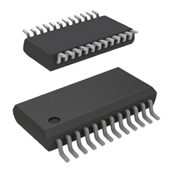
Page 176: 24-Pin Ssop (150Mil) Outline Dimensions
HT66FM5340 Brushless DC MCU with Pre-driver 24-pin SSOP (150mil) Outline Dimensions " Dimensions in inch Symbol Min. Nom. Max. — 0.236 BSC — — 0.154 BSC — 0.008 — 0.012 C’ — 0.341 BSC — — — 0.069 — 0.025 BSC —... - Page 177 However, Holtek assumes no responsibility arising from the use of the specifications described. The applications mentioned herein are used solely for the purpose of illustration and Holtek makes no warranty or representation that such applications will be suitable without further modification, nor recommends the use of its products for application that may present a risk to human life due to malfunction or otherwise.
Need help?
Do you have a question about the HT66FM5340 and is the answer not in the manual?
Questions and answers