Table of Contents
Advertisement
Quick Links
Advertisement
Table of Contents

Related Manuals for Avnet UltraZed-EG


Summary of Contents for Avnet UltraZed-EG
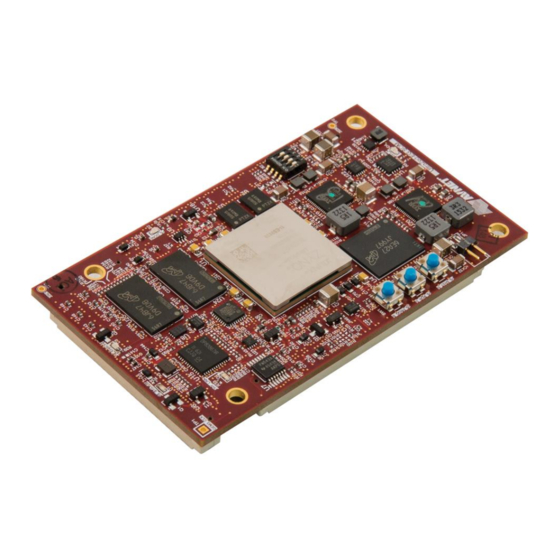
- Page 1 Accelerate Success Technology UltraZed-EG SOM Hardware User Guide Version 1.0...
- Page 2 Document Control Document Version: Version 1.0 Document Date: December 7, 2016 Document Author(s): Donny Saveski Document Classification: Public Document Distribution: Public Prior Version History: Version: Date: Comment: 12/7/16 Initial Release Comments: Version 1.0 Page 2...
-
Page 3: Table Of Contents
Contents Introduction ......................5 Functional Description ...................7 Zynq UltraScale+ MPSoC ......................7 Memory ............................ 7 2.2.1 DDR4 ........................... 7 2.2.2 Dual Parallel (x8) QSPI Flash ....................9 2.2.3 eMMC x8 Flash (Multi-Media Controller) ................10 2.2.4 SFVA625 Device Package Delay Compensation for Memory Interfaces ......11 GTR Transceivers ........................ - Page 4 2.15 Power Supplies ........................34 2.15.1 Voltage Rails and Sources ....................34 2.15.2 Voltage Regulators ......................36 2.15.3 Power Supply Sequencing and Power Modes ..............37 2.15.4 PCB Bypass / Decoupling Strategy ................... 40 2.15.5 Power Estimation ....................... 41 2.15.6 System Monitor (SYSMON) ....................41 2.15.7 Battery Backup –...
-
Page 5: Introduction
1 Introduction The UltraZed™-EG SOM (System-On Module) is a low cost System-On-Module targeted for broad use in many applications. The features provided by the UltraZed-EG System-On-Module consist of: Xilinx XCZU3EG-1SFVA625 MPSoC Pin Compatible with the 2EG, 2CG, and 3CG MPSoC devices in the same package... - Page 6 The following figure is a high level block diagram of the UltraZed-EG SOM and the peripherals attached to the Zynq UltraScale+ MPSoC Processing Sub-System and Programmable Logic Sub-System. PS-Side PL-Side HP I/O (90) DDR4 (2GB, x32) MIO[0:12] Dual QSPI (64MB)
-
Page 7: Functional Description
2 Functional Description 2.1 Zynq UltraScale+ MPSoC The UltraZed-EG SOM includes a Xilinx Zynq UltraScale+ MPSoC. The devices capable of being populated on the UltraZed-EG SOM are the XCZU2EG-1SFVA625 or XCZU3EG-1SFVA625 MPSoC. The UltraZed- EG SOM also supports the 2CG and 3CG MPSoC device as well as both extended and industrial temperature grade options as well as all of the speed grade options offered by Xilinx. - Page 8 Bank 504 Data Group Fly-by Routing DDR4 SDRAM Address/Control Group (1GB) MT40A512M16JY-083E IT:B VREF Data Group DDR4 SDRAM (1GB) TPS51200 MT40A512M16JY-083E IT:B VREF VREF Figure 3 – DDR4 Block Diagram Table 1 – DDR4 Connections Signal Name Description Bank 504 MPSoC Pin DDR4 Pin PS_DDR_A0 DDR Address Input...
-
Page 9: Dual Parallel (X8) Qspi Flash
2.2.2 Dual Parallel (x8) QSPI Flash The UltraZed-EG SOM features two 4-bit SPI (quad-SPI) serial NOR flash devices organized in a dual parallel configuration. The Micron MT25QU256ABAIEW7-0SIT QSPI Flash devices are used on the UltraZed-EG SOM. The Multi-I/O SPI Flash memory is used to provide non-volatile boot, application code, and data storage. -
Page 10: Emmc X8 Flash (Multi-Media Controller)
MPSoC via Bank 500. The eMMC I/O has direct connections to the Zynq UltraScale+ MIO through the PS_MIO [13:22] pins. The UltraZed-EG SOM end-user is capable of issuing a soft reset, P0_EMMC0_RST_N, to the eMMC flash device via an on board two-wire serial interface. The active low reset is assigned to Port 0 of the Texas Instruments TCA9534 I/O expander. -
Page 11: Sfva625 Device Package Delay Compensation For Memory Interfaces
2.3 GTR Transceivers The UltraZed-EG SOM has four multi-gigabit transceiver lanes that reside on Bank 505 of the Zynq UltraScale+ MPSoC device. These transceivers can be used to interface to multiple high speed interface protocols such as PCI Express, Serial ATA, USB3.0, and Display Port. -
Page 12: Sfva625 Device Package Delay Compensation For Gtr Transceiver Interface
Transceiver Chip is used as the PHY. The PHY features a complete HS-USB Physical Front-End supporting speeds of up to 480Mbs. VDDIO for this device can be 1.8V or 3.3V, and on the UltraZed-EG SOM VDDIO is powered at 1.8V. The PHY is connected to MIO Bank 502 which is also powered at 1.8V. This is critical Version 1.0... -
Page 13: Sfva625 Device Package Delay Compensation For Usb2.0 Interface
(configured as ULPI Output Clock Mode). On the UltraZed-EG SOM, the 24 MHz oscillator is an Abracon ASDMB CMOS oscillator, ASDMB-24.000MHZ-LY-T. The physical USB connector is not populated on the UltraZed-EG SOM. The SOM is designed to have the physical USB connector reside on the end-user carrier card. The four USB connector signals (USB_OTG_P, USB_OTG_N, USB_ID and USB_OTG_CPEN) and USB_OTG_VBUS are connected to the JX3 Micro Header. -
Page 14: 10/100/1000 Ethernet Phy
Zynq UltraScale+ MPSoC device through Bank 502. The physical RJ45 connector and magnetics is not populated on the UltraZed-EG SOM. The SOM is designed to have the physical RJ45 connector and magnetics reside on the end-user carrier card. The RJ45 connector signals are connected to the JX3 Micro Header. -
Page 15: Ethernet Phy Strapping Resistors
requires register access to the Gigabit Ethernet PHY as well as a software polling mechanism for the I/O Expander to identify interrupt activity. A high-level block diagram of the 10/100/1000 Ethernet interface is shown in the following figure. TI DP83867 10/100/1000 PHY MPSoC TX_CLK TP_P_A... -
Page 16: Ethernet Phy Leds
The following table lists the various strapping options that are available for the 10/100/1000 Ethernet PHY on the UltraZed-EG SOM and the default mode that they are strapped too. For a definition of what other options are available by changing the default mode settings, please refer to the Texas Instruments DP83867 data sheet. -
Page 17: I2C I/O Expander
2.6 I2C I/O Expander The UltraZed-EG SOM uses a Texas Instruments TCA9534PWR (16-pin TSSOP) I2C and SMBUS Low- Power I/O Expander. The Zynq UltraScale+ MPSoC controller required for I2C is named I2C1 and it exists at MIO [25:24]. Table 10 – I2C1 TRM Pin Mapping... -
Page 18: I2C Switch/Multiplexer
The I2C Switch/MUX allows for selection of control of the end-user carrier card two-wire serial interface or alternatively one could select the PMBUS interface that is tied to the UltraZed-EG SOM main multi-output power supplies as well as any device that may exist on the end-user carrier card PMBUS through the JX2 connector. -
Page 19: End-User Carrier Card I2C Interface
The UltraZed-EG SOM provides a master two-wire serial bus (CC_SDA, CC_SCL, and CC_INT_N) to the end-user carrier card via the JX3 connector so that software can communicate with all I2C devices on the UltraZed-EG SOM as well as the slave I2C devices on the end-user carrier card using a single two-wire serial interface. -
Page 20: Pmbus Interface
JX2 CONNECTOR PMBUS_SDA JX2.11 PMBUS_SCL JX2.12 P5_PMBUS_ALERT_N JX2.35 The following figure shows how the PMBus will be connected on the UltraZed-EG SOM and the UltraZed IO Carrier Card from Avnet. UltraZed-EG SOM Shunt Jumpers JP2/JP3 I2C – MIO[24:25] SDA/SCL SD1/SC1... -
Page 21: I2C Eeprom
Figure 11 – I2C EEPROM Addressing 2.9 PS General Purpose Interrupt The UltraZed-EG SOM contains a general purpose interrupt IO that is attached to PS MIO[23]. This interrupt signal will contain a pull-up to +VCCO_PSIO0_500. The interrupt output (INT#) of the Texas Instruments TCA9534 device is connected to the PS MIO [23]. -
Page 22: Io User Pins
2.10.2 PL IO User Pins The UltraZed-EG SOM provides 24 user PL IO pins from Bank 26, 52 user PL IO pins from bank 64, 52 user PL IO pins from Bank 65, and 52 user PL IO pins from Bank 66 of the Zynq UltraScale+ MPSoC. The 180 PL IO pins on the UltraZed-EG SOM connect to the Zynq UltraScale+ Programmable Logic Sub-System for user implementation of most any feasible interface. -
Page 23: Control Signal Sources
This signal resets every register in the device capable of being reset. On UltraZed-EG SOM, this signal is labelled PS_POR_B and it is connected to push button, SW3. To stall Zynq UltraScale+ MPSoC boot-up, this signal should be held low. No other signal (PS_SRST_B, PROGRAM_B, or INIT_B) is capable of doing this as in other Xilinx FPGA architectures. -
Page 24: Processor Subsystem Reset (Ps_Srst_B) And Som Reset (Som_Reset_In_N)
The system reset, labelled PS_SRST_B, resets the processor as well as erases all debug configurations. On UltraZed-EG SOM, this signal is labelled PS_SRST_B and it is connected to push button, SW4. The UltraZed-EG SOM end-user is also capable of being issued an external system reset from the end-user carrier card via the JX2 Connector signal SOM_RESET_IN_N. - Page 25 Bank 66 Single Ended I/Os Zynq UltraScale+ Bank 66 Bank 65 Differential Pair I/Os Zynq UltraScale+ Bank 65 Bank 66 Differential Pair I/Os Zynq UltraScale+ Bank 66 PMBUS Carrier Card or UltraZed-EG SOM SOM_PG_OUT UltraZed-EG SOM Control CC_RESET_OUT_N UltraZed-EG SOM SOM_RESET_IN...
-
Page 26: Jx Connector Master Table
USB_OTG_VBUS Voltage Feedback Sense Pins UltraZed-EG SOM TOTAL 2.13.2 JX Connector Master Table The following tales list the UltraZed-EG SOM JX Connectors connections in master tables targeting each connector. Table 25 –JX1 Connector Master Table Zynq Pin UltraZed-EG Net JX1 Pin... - Page 27 JX1_HP_DP_08_N JX1_HP_DP_11_P JX1_HP_DP_10_P JX1_HP_DP_11_N JX1_HP_DP_10_N JX1_HP_DP_13_P JX1_HP_DP_12_P JX1_HP_DP_13_N JX1_HP_DP_12_N JX1_HP_DP_15_P JX1_HP_DP_14_P JX1_HP_DP_15_N JX1_HP_DP_14_N JX1_HP_DP_17_P JX1_HP_DP_16_P JX1_HP_DP_17_N JX1_HP_DP_16_N JX1_HP_DP_19_GC_P JX1_HP_DP_18_GC_P JX1_HP_DP_19_GC_N JX1_HP_DP_18_GC_N JX1_HP_DP_21_GC_P JX1_HP_DP_20_GC_P JX1_HP_DP_21_GC_N JX1_HP_DP_20_GC_N JX1_HP_DP_23_P JX1_HP_DP_22_P JX1_HP_DP_23_N JX1_HP_DP_22_N JX1_HP_DP_25_P JX1_HP_DP_24_P JX1_HP_DP_25_N JX1_HP_DP_24_N JX1_HP_DP_27_P JX1_HP_DP_26_P JX1_HP_DP_27_N JX1_HP_DP_26_N JX1_HP_DP_29_P JX1_HP_DP_28_P JX1_HP_DP_29_N JX1_HP_DP_28_N JX1_HP_DP_31_P JX1_HP_DP_30_P...
- Page 28 JX1_HP_DP_39_N JX1_HP_DP_38_N JX1_HP_DP_41_P JX1_HP_DP_40_P JX1_HP_DP_41_N JX1_HP_DP_40_N JX1_HP_SE_01 JX1_HP_SE_00 JX1_HP_SE_03 JX1_HP_SE_02 JX1_HP_SE_05 JX1_HP_SE_04 Table 26 – JX2 Connector Master Table Zynq Pin UltraZed-EG Net JX2 Pin UltraZed-EG Net Zynq Pin Number Name Number Name Number SYSMON_V_N SYSMON_DX_N SYSMON_V_P SYSMON_DX_P JX2_HD_SE_00_P JX2_HD_SE_01_P...
- Page 29 JX2_HP_DP_03_P JX2_HP_DP_02_P JX2_HP_DP_03_N JX2_HP_DP_02_N JX2_HP_DP_05_P JX2_HP_DP_04_P JX2_HP_DP_05_N JX2_HP_DP_04_N JX2_HP_DP_07_P JX2_HP_DP_06_P JX2_HP_DP_07_N JX2_HP_DP_06_N JX2_HP_DP_09_P JX2_HP_DP_08_P JX2_HP_DP_09_N JX2_HP_DP_08_N JX2_HP_DP_11_GC_P JX2_HP_DP_10_GC_P JX2_HP_DP_11_GC_N JX2_HP_DP_10_GC_N JX2_HP_DP_13_GC_P JX2_HP_DP_12_GC_P JX2_HP_DP_13_GC_N JX2_HP_DP_12_GC_N JX2_HP_DP_15_P JX2_HP_DP_14_P JX2_HP_DP_15_N JX2_HP_DP_14_N JX2_HP_DP_17_P JX2_HP_DP_16_P JX2_HP_DP_17_N JX2_HP_DP_16_N JX2_HP_DP_19_P JX2_HP_DP_18_P JX2_HP_DP_19_N JX2_HP_DP_18_N JX2_HP_DP_21_P JX2_HP_DP_20_P JX2_HP_DP_21_N JX2_HP_DP_20_N JX2_HP_DP_23_P JX2_HP_DP_22_P JX2_HP_DP_23_N...
- Page 30 JX2_HP_DP_28_P JX2_HP_DP_29_N JX2_HP_DP_28_N JX2_HP_SE_01 JX2_HP_SE_00 JX2_HP_SE_03 JX2_HP_SE_02 JX2_HP_SE_05 JX2_HP_SE_04 Table 27 – JX3 Connector Master Table Zynq Pin UltraZed-EG Net JX3 Pin UltraZed-EG Net Zynq Pin Number Name Number Name Number GTR_TX3_P GTR_TX3_N GTR_RX3_P GTR_RX3_N GTR_TX2_P GTR_TX2_N GTR_RX2_P GTR_RX2_N GTR_TX1_P...
- Page 31 ETH_MD3_P ETH_MD4_N ETH_MD3_N G14, E13, D15 VCCO_PSIO_501 CC_INT_N MIO_26 MIO_27 MIO_28 MIO_29 MIO_30 MIO_31 MGTRAVCC_Sense MGTRAVTT_Sense MIO_32 MIO_33 MIO_34 MIO_35 MIO_36 MIO_37 VCCO_HP_66_Sense VCCO_HD_26_Sense MIO_38 MIO_39 MIO_40 MIO_41 MIO_42 MIO_43 VCCO_HP_65_Sense VCCO_HP_64_Sense MIO_44 MIO_45 MIO_46 MIO_47 MIO_48 MIO_49 MIO_50 MIO_51 Table 28 –...
-
Page 32: Powering The Pl Banks (Som_Pg_Out)
2.13.3 Powering the PL Banks (SOM_PG_OUT) The UltraZed-EG SOM does not power the PL VCCIO banks. This is required to be provided by the end- user carrier card. This gives the end-user carrier card the flexibility to control the I/O bank voltages depending on the interfaces the end-user decides to implement. -
Page 33: Jtag Connections
DONE LED will illuminate. 2.14.1 JTAG Connections The UltraZed-EG SOM requires an external JTAG cable connector populated on the carrier card for JTAG operations. JTAG signals are routed from Bank 503 of the Zynq UltraScale+ MPSoC to the Micro Header JX1. -
Page 34: Power Supplies
UltraZed-EG SOM. Most of these regulators are powered from the end-user carrier card via the +VIN pins on the Micro Headers and are expected to carry +5V or +12V to the UltraZed-EG SOM regulator inputs. There are also four bank voltages that are supplied from the end-user carrier card to the UltraZed-EG SOM. - Page 35 Table 31 – UltraZed-EG SOM Voltage Rails Schematic Voltage Voltage Level Zynq Connection Voltage Name Origination +5VREG 5.0V +2.5V 2.5V +DDR4_VREF 1.2V +1.0V 1.0V +DDR4_VTT 0.6V VCCO_PSIO0_500 VCCO_PSIO2_502 VCCO_PSIO3_503 +VCCO_PSIO 1.8V VCC_PSADC VCC_PSAUX VCCAUX UltraZed-EG VCCAUX_IO +VCCAUX 1.8V VCCADC +VCC_PSINTLP 0.85V...
-
Page 36: Voltage Regulators
ADP223 regulator completing the power sequence. These two supplies are the last regulators to be brought The UltraZed-EG SOM provides a power good signal to the end-user carrier card to signal that the SOM power sequencing has completed and the end-fuser carrier card is free to bring up the VCCO supplies. This signal is called SOM_PG_OUT and is tied to JX2.Pin 41. -
Page 37: Power Supply Sequencing And Power Modes
Table 32 – Voltage Rails Max Current and Power Modes Power Modes Voltage Power Voltage Rail Current (A) Domain Full PS Low Power Only Power +5VREG 5.0V 0.5A +2.5V 2.5V 0.3A +DDR4_VREF 1.2V 0.04A +1.0V 1.0V 0.3A +DDR4_VTT 0.6V 5.5A +VCCO_PSIO 1.8V 0.5A *... - Page 38 Upon repowering these domains, proper sequencing should again be followed. The following diagrams are indicative of the pre-programmed power-on and power-off sequences that exist on the UltraZed-EG SOM and the UltraZed IO Carrier Card. Version 1.0 Page 38...
- Page 39 Figure 15 – UltraZed Power-On Sequence Figure 16 – UltraZed Power-Off Sequence Version 1.0 Page 39...
-
Page 40: Pcb Bypass / Decoupling Strategy
Figure 17 – Power-Up Flow with Carrier Card 2.15.4 PCB Bypass / Decoupling Strategy The UltraZed-EG SOM design follows at a minimum the PCB decoupling strategy as outlined in UG583 for the Zynq UltraScale+ MPSoC in the SFVA625 package. NOTE: These quantities are considered preliminary and subject to change because power and package modelling is still in progress at Xilinx. -
Page 41: Power Estimation
When designing the UltraZed-EG SOM architecture, the XPE tool was used to ensure that the UltraZed-EG SOM system could supply enough power to the Zynq UltraScale+ and its on-board peripherals using worst case parameters including logic utilization, operating frequency and temperature while still supporting low power modes and various speed grade options. -
Page 42: Battery Backup - Device Secure Boot Encryption Key
The encryption key can alternatively be stored in eFuse which does not require a battery. On the UltraZed-EG SOM, +PS_VBATT is interfaced to the JX3 connector relying on the end-user carrier card to properly implement the battery functionality. To apply an external battery to Zynq UltraScale+... -
Page 43: Thermal Management: Heatsink And Fan Assembly
This 3-pin keyed connector is .100” pitch and has the 5V conductor as pin 2 on the connector. For reference, the fan supplied with the UltraZed-EG SOM mates with the fan header on the UltraZed IO Carrier Card. -
Page 44: Zynq Ultrascale+ Mpsoc I/O Bank Allocation
3 Zynq UltraScale+ MPSoC I/O Bank Allocation 3.1 PS MIO Bank Allocation There are 78 I/O available in the PS MIO Banks. The tables below lists the number of required I/O per peripheral and the MIO locations where the interface exists. Table 35 –... -
Page 45: Zynq Ultrascale+ Mpsoc Bank Voltages
PL I/O Banks 26, 64, 65, and 66 are powered from the end-user carrier card. These bank supplies are designed to be independent on the UltraZed-EG SOM. Maximum flexibility is allowed to the designer for these banks as the voltage level and standards are left to the end-user carrier card design. The designer of the end-user carrier card VCCO supplies is provided the choice of whether the IO banks use a shared voltage supply or independent voltage supplies. -
Page 46: Mechanical
4 Mechanical The UltraZed-EG SOM measures 2.00” x 3.50” (50.80 mm x 88.9 mm). Figure 21 – UltraZed-EG SOM Top View Mechanical Dimensions Version 1.0 Page 46... - Page 47 Figure 22 – UltraZed-EG SOM Side View Mechanical Dimensions The UltraZed-EG SOM is populated with an active fan and heatsink combination that has a maximum vertical dimension of 1.750” (44.45 mm). The Heatsink is available in many other sizes, but the minimum vertical dimension of the fan and heatsink combination using the smallest heatsink is 0.750”...
Need help?
Do you have a question about the UltraZed-EG and is the answer not in the manual?
Questions and answers