Table of Contents
Advertisement
Quick Links
Advertisement
Table of Contents

Related Manuals for Avnet Qorvo


Summary of Contents for Avnet Qorvo
- Page 1 Qorvo 1800MHz Small Cell RF Card Hardware User’s Guide Version 1.3 Page 1 Copyright © 2019 Avnet, Inc. AVNET, “Reach Further,” and the AV logo are registered trademarks of Avnet, Inc. All other brands are the property of their respective owners.
-
Page 2: Table Of Contents
Directional Coupler ........................ 32 5.15 Circulator ..........................32 Regulatory and Compliance Information ............. 33 Getting Help and Support ..................34 Appendix A – Alternate Reverse Build Variant ............ 35 Page 2 Qorvo 1800MHz Small Cell RF Card Hardware User’s Guide... -
Page 3: Document Control
11 November 2019 2 Version History Version Date Comment 24 Oct 2019 Initial Release Added detail to Appendix A – Alternate Reverse Build Variant 11 Nov 2019 Page 3 Qorvo 1800MHz Small Cell RF Card Hardware User’s Guide Hardware User’s Guide... -
Page 4: Introduction
The ZCU111 has an XCZU28DR Zynq RFSoC device with eight 12-bit ADC’s that can operate up to 4GHZ and eight 14-bit DAC’s that can operate up to 6.5GHz. The Qorvo uses 4 ADC channels and 2 DAC channels in order to support a 2x2 configuration with observation paths for digital pre-distortion (DPD). -
Page 5: Zynq Ultrascale+ Rfsoc Development Kit
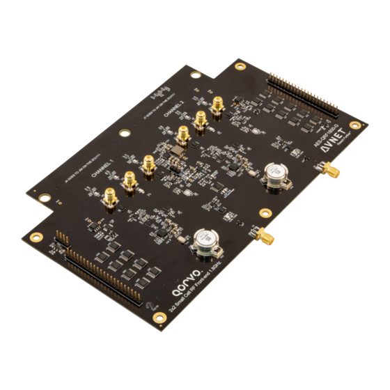
Qorvo. We extend the functionality of the Xilinx Zynq UltraScale+ RFSoC ZCU111 Evaluation Kit by adding a Qorvo 2x2 Small Cell RF front-end 1.8 GHz card for over-the- air transmission, plus native connection to MATLAB® & Simulink® with Avnet's RFSoC Explorer®... -
Page 6: Glossary
Zynq UltraScale+ RFSoC Processing System Radio Frequency RFMC RF Mezzanine Card RFSoC Radio Frequency System-on-Chip Root Mean Square Receive Serial Addressable Mode Serial Peripheral Interface Transmit Tool Command Language Page 6 Qorvo 1800MHz Small Cell RF Card Hardware User’s Guide Hardware User’s Guide... -
Page 7: Reference Documents
Reference Documents ZCU111 Evaluation Board User Guide AES-QRF1800-G Schematic for Qorvo 2x2 Small Cell RF Front-end 1.8GHz Xilinx Vivado Design Suite Xilinx Software Development Kit Zynq UltraScale+ RFSoC RF Data Converter 2.1 LogiCORE IP Product Guide (PG269) Zynq UltraScale+ RFSoC Data Sheet: DC and AC Switching Characteristics (DS926) Page 7 Qorvo 1800MHz Small Cell RF Card Hardware User’s Guide... -
Page 8: Architecture And Features
TQQ0302 - 1747.5 MHz RF BAW Filter - Band 3 Uplink TQP4M9017 - Fast Digital Step Attenuator RMS Power Detector QPL9096 - Ultra Low-Noise Bypass LNA Page 8 Qorvo 1800MHz Small Cell RF Card Hardware User’s Guide Hardware User’s Guide... -
Page 9: Block Diagram
Block Diagram Figure 3 – Block Diagram Page 9... -
Page 10: Functional Description
The following sections provide brief descriptions of each feature provided on the board. ZCU111 Interface Two Samtec RFMC (RF Mezzanine Card) LPAM connectors on the Qorvo RF card plug into the corresponding LPAF connectors on the ZCU111. These connectors carry the analog I/O associated with RFSoC, as well as the digital control signals. -
Page 11: Digital Isolation
ZCU111 and Qorvo card are powered separately as in the diagram below, the digital ground from the ZCU111, DGND, is not connected to the Qorvo card’s RF ground, RGND. Note that this is not the factory default power configuration and that here external 5V to the Qorvo card requires R140 and R141 to be removed. -
Page 12: Power Options
Figure 7 – Factory Default Configuration with 12V from the ZCU111 It is also possible to power the Qorvo card stand-alone on the bench, from either 12V or 5V. The power options all require various resistor configurations. The table on sheet 11 of the schematic [2] clearly specifies which resistors need to be placed or removed for each option. -
Page 13: Attenuators Digital Step Attenuator (Dsa) Devicescontrol Interfaces
Figure 9 – Addressing and Timing for the Serial Addressable Mode Interface Page 13 Qorvo 1800MHz Small Cell RF Card Hardware User’s Guide Hardware User’s Guide... - Page 14 Figure 10 – Attenuator Control Interfaces Page 14 Qorvo 1800MHz Small Cell RF Card Hardware User’s Guide Hardware User’s Guide...
- Page 15 The programmable logic and software in the Avnet reference design implements the serial protocol for these attenuators. See 5.5. The image below shows data being clocked out to one of the attenuators on the Channel 1 serial bus. The serial clock here is 5MHz. The first signal, LE, is the latch enable signal, which toggles after the serial data in (SI) has been clocked in.
-
Page 16: Rebuilding The Reference Design
Avnet RFSoC Kit is on GitHub. This reference design is for the ZCU111 interfaced with the Qorvo card. It is a Vivado project that can be re-built from sources in the online repository, using the instructions that are also in the repository. -
Page 17: Spi Controller
DSA’s and other digital signals. This can be done through a serial port or, ultimately, from MathWorks. The Avnet reference design (see 5.5) software implementation uses the spidev Linux driver. The Vivado project instantiates an axi_quad_spi component and the custom qorvo_spi component that maps the interface to the control signals. -
Page 18: Gpio Assignments
The table below shows how the GPIO pins have been assigned. Note that the Zynq firmware pin number assignments can be found in the Vivado project file qorvo_spi_slave.xdc. This file can be found in the Avnet reference design (see 5.5) inside the pl\qorvo1800\revB\src folder. Table 1 – Assignments for Digital GPIO from the ZCU111... - Page 19 Ch2 Rx DSA Data bit 4 ADCIO_18 AV2 J47 pin H3 CH2_RX_DSA_D5X J6 pin 10 Ch2 Rx DSA Data bit 5 ADCIO_19 AV3 J47 pin H5 Spare Page 19 Qorvo 1800MHz Small Cell RF Card Hardware User’s Guide Hardware User’s Guide...
-
Page 20: Eeprom And I2C Interface
EEPROM and I2C Interface U66 on the Qorvo card is 1Kbit EEPROM from Microchip. It uses a 2-wire I2C interface. purpose of this device is to store a board ID so that software can distinguish this board from other daughter card. It would also be possible to store a device ID and/or calibration parameters that are unique to a specific board’s serial number. -
Page 21: Digital Test Pins
Ch2 Rx DSA Data bit 1 J1 pin 7 CH1_RX_DSA_D2X Ch2 Rx DSA Data bit 2 J1 pin 8 CH1_RX_DSA_D3X Ch2 Rx DSA Data bit 3 Page 21 Qorvo 1800MHz Small Cell RF Card Hardware User’s Guide Hardware User’s Guide... - Page 22 Ch2 Tx PA Enable J6 pin 12 CH2_TX_LNA_DISX Ch2 Tx LNA Disable J6 pin 13 CH2_RX_LNA0_BYPX Ch2 Rx LNA0 Bypass J6 pin 14 CH2_RX_LNA1_BYPX Ch2 Rx LNA1 Bypass Page 22 Qorvo 1800MHz Small Cell RF Card Hardware User’s Guide Hardware User’s Guide...
-
Page 23: Status Leds
Table 4 – Status LEDs Color Description Ch1 Rx LNA0 Overload (see 5.13.1) Ch2 Rx LNA0 Overload (see 5.13.1) Yellow Software-controlled Comms indicator Green Power Good Page 23 Qorvo 1800MHz Small Cell RF Card Hardware User’s Guide Hardware User’s Guide... -
Page 24: Rfmc Connector Pin Assignments
(table 3-21 of the ZCU111 Board User Guide [1]). Figure 16 – RFMC DAC LPAF Connector J94, Vertical Orientation (A1 Upper Right Corner) Page 24 Qorvo 1800MHz Small Cell RF Card Hardware User’s Guide Hardware User’s Guide... - Page 25 Figure 17 – RFMC RF-ADC LPAF Connector J47, Vertical Orientation (A1 in Upper Right Corner) Page 25 Qorvo 1800MHz Small Cell RF Card Hardware User’s Guide Hardware User’s Guide...
- Page 26 The tables below show the Qorvo-side connector pin assignments for the RFMC LPAM connectors. Table 5 – Channel 1 RFMC J4 (mates with ZCU111 J94) Conn. Pin # ZCU111 ZCU111 Qorvo Chip Pin # Signal Name Signal Name UTIL_3V3 VBUS_1V8...
- Page 27 Table 6 – Channel 2 RFMC J7 (mates with ZCU111 J47) Conn. Pin # ZCU111 ZCU111 Qorvo Chip Pin # Signal Name Signal Name ADCIO_00 COMMS_LEDX ADCIO_01 VBUS_1V8 UTIL_3V3 ADCIO_02 CH2_RX_LNA0_BYPX Page 27 Qorvo 1800MHz Small Cell RF Card Hardware User’s Guide Hardware User’s Guide...
- Page 28 ADCIO_06 CH2_RX_OVX VBUS_1V8 UTIL_3V3 ADC_01_P ADC_03_P ADC_05_P ADC_07_P ADCIO_07 CH2_TX_PA_ENX ADCIO_08 CH2_RX_LNA1_DISX ADCIO_09 CH2_TX_LNA_DISX UTIL_3V3 ADCIO_10 CH2_LEX ADCIO_11 CH2_CLKX UTIL_3V3 ADCIO_12 CH2_SIX ADCIO_13 CH2_RX_DSA_D0X ADCIO_14 CH2_RX_DSA_D1X Page 28 Qorvo 1800MHz Small Cell RF Card Hardware User’s Guide Hardware User’s Guide...
-
Page 29: Pi Pad Attenuators
UTIL_3V3 5.12 Pi Pad Attenuators There are –2 dB balanced Pi pad attenuators on the Qorvo card PCB between the RFSoC ADC/DAC connections within the SAMTEC LPAF connector and the baluns on the Qorvo card. Resistor values are shown below. Also note the 100 nF AC coupling capacitors. -
Page 30: Adc Input Protection
Figure 19- Rx-Side ADC over-voltage protection Page 30 Qorvo 1800MHz Small Cell RF Card Hardware User’s Guide The RF-ADC input buffer contains an internal over voltage feature offering protection for signals in the range defined in the Zynq UltraScale+ RFSoC Data Sheet: DC and AC Switching Characteristics (DS926). Full-scale input voltage Hardware User’s Guide... -
Page 31: Rx Lna Bypass Mechanisms
ZCU111 GPIO signals through LPAF/M, and the comparator and AD8361 power detector. These signals are also routed to the Digital Test Pins, for scenarios where the Qorvo card may be used in standalone mode within a test harness independent of the ZCU111. -
Page 32: Directional Coupler
(port 2 to port 3) and then the duplexer. This topology removes the circulator from the Rx path altogether. Figure 22 – DPD path Directional Coupler and Circulator Page 32 Qorvo 1800MHz Small Cell RF Card Hardware User’s Guide Hardware User’s Guide... -
Page 33: Regulatory And Compliance Information
6 Regulatory and Compliance Information The Qorvo card can radiate radio frequency energy and has not been tested for CE, FCC, or IC compliance. The intended use is for demonstration, engineering development, or evaluation purposes. There are no constraints on operating temperature range, beyond thermal relief experimentation. -
Page 34: Getting Help And Support
7 Getting Help and Support If additional support is required, Avnet has many avenues to search depending on your needs. For documentation, technical specifications, and videos visit the Avnet RFSoC kit page: www.avnet.com/rfsockit If you have questions, please use the RFSoC Kit forum on our Element 14 ZedBoard Community page: https://www.element14.com/zedboardcommunity... -
Page 35: Appendix A - Alternate Reverse Build Variant
8 Appendix A – Alternate Reverse Build Variant The Qorvo Card is a 2-channel FDD system with duplexers and filters tuned for specific uplink (RX) and downlink (TX) center frequencies. Both channels are identical in the production build. Downlink means a signal transmitted from the DAC of RFSoC , through the TX signal chain of the Qorvo card, to a user-equipment radio receiver ... - Page 36 RF Transmit Channel 2 requires the capacitor swap on the REVERSE variant Figure 24 – Normal RF Transmit Channel 2 Figure 25 – Reverse RF Transmit Channel 2 Page 36 Qorvo 1800MHz Small Cell RF Card Hardware User’s Guide Hardware User’s Guide...
- Page 37 The NORMAL configuration is how the board arrives from the manufacturer. The REVERSE configuration is an optional way to configure the card, but requires modification to the board which will void the standard warranty for the Qorvo card. Only attempt these changes if you have adequate board rework equipment and expertise.
Need help?
Do you have a question about the Qorvo and is the answer not in the manual?
Questions and answers