
Related Manuals for ADLINK Technology PXIe-3985


Summary of Contents for ADLINK Technology PXIe-3985
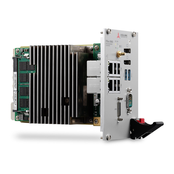
- Page 1 PXIe-3985 PXI Express Embedded Controller User’s Manual Manual Rev.: 2.00 Revision Date: Feb. 4, 2015 Part No: 50-17048-1000 Advance Technologies; Automate the World.
- Page 2 Revision History Revision Release Date Description of Change(s) 2.00 2015/2/4 Initial Release...
-
Page 3: Preface
PXIe-3985 Preface Copyright 2015 ADLINK TECHNOLOGY, INC. This document contains proprietary information protected by copy- right. All rights are reserved. No part of this manual may be repro- duced by any mechanical, electronic, or other means in any form without prior written permission of the manufacturer. - Page 4 ® ® ® 98, Windows NT, Windows 2000, Windows XP, and ® ® ® Windows Vista are registered trademarks of Microsoft Corporation. PCI™, is a registered trademark of the Peripheral Component Interconnect Special Interest Group (PCI-SIG). Product names mentioned herein are used for identification pur- poses only and may be trademarks and/or registered trademarks of their respective companies.
-
Page 5: Table Of Contents
2 Getting Started ..............17 Package Contents ............. 17 Operating System Installation..........18 2.2.1 Installation Environment ........... 19 2.2.2 Installing the PXIe-3985 ........... 20 2.2.3 Replacing the Hard Drive or Solid State Drive ..21 2.2.4 Replacing the Battery Backup ........22 2.2.5... - Page 6 3 Driver Installation............. 25 Installing Windows Drivers..........25 Installing the Chipset Driver ..........25 Installing the Graphics Driver..........26 Installing the Ethernet Driver..........26 Installing the GPIB Driver........... 27 Installing the Management Engine Driver ......27 Installing the PXI Trigger Driver ......... 28 Installing the USB 3.0 Driver..........
- Page 7 PXIe-3985 Getting Service..............49...
- Page 8 This page intentionally left blank. viii...
-
Page 9: List Of Figures
PXIe-3985 List of Figures Figure 1-1: PXIe-3985 Functional Block Diagram......3 Figure 1-2: PXIe-3985 Front Panel ............ 7 Figure 1-3: PXI Trigger SMB Jack ............. 8 Figure 1-4: DisplayPort Connector............. 9 Figure 1-5: PXIe-3985 LED Indicators ..........11 Figure 1-6: COM Port............... 14 Figure 1-7: PXIe-3985 Onboard Configuration ........ - Page 10 This page intentionally left blank. List of Figures...
-
Page 11: List Of Tables
Table 1-4: LED Indicator Legend ............ 11 Table 1-5: USB 2.0 Port Pin Assignment........12 Table 1-6: PXIe-3985 Ethernet Port Pin Assignments....12 Table 1-7: D-Sub 9p COM Port Signal Functions ......14 Table 1-8: Onboard Configuration Legend ........15 Table B-1: BIOS Hot Key Functions.......... - Page 12 This page intentionally left blank. List of Tables...
-
Page 13: Introduction
PXIe-3985 utilizes four separate computing engines on a single processor, enabling execution of four independent tasks simulta- neously. With a configurable PCIe switch, the PXIe-3985 can sup- port four links x4 or two links x16 x8 PXI Express link capability, with maximum system throughput of up to 8 GB/s. -
Page 14: Features
1.1 Features -5 PXI Express Hardware Specification Rev.1.0 ® Intel Core™ i7-4700EQ 2.4 GHz processor for maximum computing power, 3.4GHz maximum in single-core, Turbo Boost mode. Dual Channel DDR3L SODIMM Up to 16 GB 1600 MHz Maximum System Throughput 8 GB/s PXI Express Link Capability 4 Four Links Configuration: x4 x4 x4 x4 2 Two Links Configuration: x16 x8... -
Page 15: Specifications
COM Port LPC- COM Port connector Trigger Bus Trigger Bus Trigger Signal Connector Controller Figure 1-1: PXIe-3985 Functional Block Diagram Processor ® Intel Core™ i7-4700EQ 2.4GHz processor DMI (Direct Media Interface) with 5 GT/s bandwidth in each direction Chipset ®... - Page 16 Supports 1333/1600MHz RAM up to 16 GB total Supports non-ECC, unbuffered memory The externally accessible SODIMM socket can accept replace- ment DDR3L DRAM DIMM modules. PXIe-3985 specifications and stability guarantees are only sup- NOTE: NOTE: ported when ADLINK-provided DDR3L DRAM DIMM modules are used.
- Page 17 PXIe-3985 Four USB 2.0 and two USB 3.0 ports on the faceplate. GPIB Onboard IEEE488 GPIB controller through Micro-D 25-pin con- nector on the faceplate. Trigger I/O One SMB connector on the faceplate to route an external trigger signal to/from PXI trigger bus...
- Page 18 ADLINK-provided SSD/HDD NOTE: NOTE: Certification Electromagnetic compatibility: EMC/EMI: CE, FCC Class A CE Compliance EN 61326-1 The PXIe-3985 meets the essential requirements of applicable European Directives. Power Requirements Voltage Rail 5V standby 3.3V Maximum power 0.13A 3.0A 3.9A...
-
Page 19: I/O And Indicators
PXIe-3985 1.3 I/O and Indicators 1.3.1 Front Panel Figure 1-2: PXIe-3985 Front Panel PXI Trigger Connector 4X Type-A USB 2.0 (SMB jack) connectors 2X DisplayPort Connectors G 2X Gigabit Ethernet GPIB Connector 2X USB 3.0 (Micro D-Sub 25P) Reset Button... -
Page 20: Figure 1-3: Pxi Trigger Smb Jack
The PXI trigger connector is a SMB jack, used to route external trigger signals to or from the PXI backplane. Trigger signals are TTL-compatible and edge sensitive. The PXIe-3985 provides four trigger routing modes from/to the PXI trigger connector to synchro-... -
Page 21: Figure 1-4: Displayport Connector
PXIe-3985 Figure 1-4: DisplayPort Connector Signal Pin Signal CN_DDPx0+ CN_DDPx3- CN_DDPx0- CN_DDPx_AUX_SEL CN_DDPx1+ CN_DDPx_CONFIG2 CN_DDPx_AUX+ CN_DDPx1- CN_DDPx2+ CN_DDPx_AUX- CN_DDPx_HPD CN_DDPx2- CN_DDPx3+ +V3.3_DDPx_PWR Table 1-2: DisplayPort Pin Assignment Introduction... -
Page 22: Gpib Connector
1.3.2 GPIB Connector The GPIB connector on PXIe-3985 is a micro D-sub 25P connec- tor, controlling external bench-top instruments. Connection other instruments requires the optional ACL-IEEE488-MD1-A cable. The on-board GPIB controller provides: Full compatibility with IEEE 488 standard Up to 1.5MB/s data transfer rates Onboard 2 KB FIFO for read/write operations Driver APIs are compatible with NI-488.2 driver software... -
Page 23: Reset Button
Table 1-4: LED Indicator Legend 1.3.5 USB 2.0 Ports The PXIe-3985 provides four USB 2.0 ports via USB Type A con- nectors on the faceplate, all compatible with hi-speed, full-speed and low-speed USB devices. Supported boot devices include USB flash drive, USB floppy, USB CD-ROM, and others, with boot pri-... -
Page 24: Gigabit Ethernet Ports
Signal Power 5V USB Data- USB Data + Ground Table 1-5: USB 2.0 Port Pin Assignment 1.3.6 Gigabit Ethernet Ports Dual Gigabit Ethernet connection is provided on the PXIe-3985 front panel. 1000Base-T Signal 100/10Base-T Signal MDI0+ MDI0- MDI1+ MDI2+ Reserved... -
Page 25: Usb 3.0 Ports
1000 Mbps 1.3.7 USB 3.0 Ports The PXIe-3985 provides two Type A USB 3.0 ports on the front panel, supporting SuperSpeed, Hi-Speed, full-speed, and low-speed transmission for downstream. Multiple boot devices, including USB flash, USB external HD, and USB CD-ROM drives are supported, with boot priority configured in BIOS. -
Page 26: Com Port
1.3.8 COM Port A COM port on the front panel with D-sub 9P connectors supports RS-232/RS-422/RS-485 by BIOS selection. Figure 1-6: COM Port Signal Name RS-232 RS-422 RS-485 DCD# TXD422- 485DATA- TXD422+ 485DATA+ RXD422+ DTR# RXD422- DSR# RTS# CTS# Table 1-7: D-Sub 9p COM Port Signal Functions Introduction... -
Page 27: Onboard Connections And Settings
PXIe-3985 1.3.9 Onboard Connections and Settings Figure 1-7: PXIe-3985 Onboard Configuration SATA Connector Clear CMOS switch System Battery Table 1-8: Onboard Configuration Legend Introduction... - Page 28 This page intentionally left blank. Introduction...
-
Page 29: Getting Started
This chapter describes procedures for installing the PXIe-3985 and making preparations for its operation, including hardware and software setup. Please note that the PXIe-3985 is shipped with RAM and HDD or SSD preinstalled. Please contact ADLINK or authorized dealer if there are any problems during the installation. -
Page 30: Operating System Installation
For other OS support, please contact ADLINK Most operating systems require initial installation from a hard drive, floppy drive, or CD-ROM drive. The PXIe-3985 controller supports USB CD-ROM drive, USB flash disk, USB external hard drive, or a USB floppy drive as the first boot device. Please see Section B.4: Boot Setup for information about setting the boot... -
Page 31: Installation Environment
Flat-head screwdriver Anti-static wrist strap Anti-static mat ADLINK PXIe-3985 system controllers are electrostatically sensitive and can be easily damaged by static electricity. The equipment must be handled on a grounded anti-static mat, and operators must wear an anti-static wristband, grounded at the same point as the anti-static mat. -
Page 32: Installing The Pxie-3985
PXIe-3985 into the chas- sis, as shown 4. Elevate the latch until the PXIe-3985 is fully seated in the chassis backplane. The alignment pin on the rear of the latch can be threaded into the best fit alignment port in the chassis rail. -
Page 33: Replacing The Hard Drive Or Solid State Drive
PXIe-3985 2.2.3 Replacing the Hard Drive or Solid State Drive The PXIe-3985 provides a SATA 3.0 port with a pre-installed 2.5" SATA hard drive or solid state drive. Replacing the HDD or SSD is accomplished as follows. 1. Locate the five screws attaching the hard drive hous- ing to the PXIe-3985 controller, as shown. -
Page 34: Replacing The Battery Backup
2.2.4 Replacing the Battery Backup The PXIe-3985 is provided with a 3.0 V “coin cell” lithium battery, replacement of which is as follows. 1. Turn off the PXI chassis. 2. Remove the PXIe-3985 embedded controller from the chassis. Observe all anti-static precautions. - Page 35 PXIe-3985 to Clear position and wait for 5 seconds, then return the switch to Normal position. 4. Remount the controller into the PXI chassis. 5. Press "Delete" or "F2" to enter the BIOS setup when the splash logo appears. 6. Press "F3" to load Optimized defaults in BIOS setup 7.
- Page 36 This page intentionally left blank. Getting Started...
-
Page 37: Driver Installation
9. Install the SMBus driver 10.Install the RST driver 3.2 Installing the Chipset Driver This section describes installation of the chipset driver for PXIe-3985. The chipset driver directs the operating system to con- ® figure the Intel QM87 chipset components. -
Page 38: Installing The Graphics Driver
The Win7 64-bit chipset driver is located in the directory: x:\Driver Installation\PXI Platform\PXI control- ler\PXIe-3985\Win7_64bit\Chipset\ 3. Execute setup.exe and follow on-screen instructions to complete the setup 4. Reboot the system 3.3 Installing the Graphics Driver To install the graphics driver: 1. -
Page 39: Installing The Gpib Driver
4. Reboot the system 3.5 Installing the GPIB Driver The PXIe-3985 controller features an onboard GPIB controller, providing connectivity between PXI and GPIB instruments. The GPIB driver package also contains function libraries and a utility to interact with GPIB instruments. -
Page 40: Installing The Pxi Trigger Driver
4. Reboot the system 3.7 Installing the PXI Trigger Driver The PXIe-3985 controller provides a trigger I/O on the faceplate to route the trigger signal to and from the PXI trigger bus. Please see Appendix A: PXI Trigger I/O Function Reference for programming information. -
Page 41: Installing The Usb 3.0 Driver
PXIe-3985 3.8 Installing the USB 3.0 Driver The PXIe-3985 controller provides two USB 3.0 ports on the face- plate. To install the USB 3.0 drivers: 1. Close any running applications. 2. Insert the ADLINK All-in-One CD (x: denotes the CD- ROM drive) The Win7 32-bit USB 3.0 driver is located in the direc-... -
Page 42: Installing The Rst Driver
2. Insert the ADLINK All-in-One CD (x: denotes the CD- ROM drive) The 32bit Win7 RST driver is located in the directory x:\ Driver Installation\PXI Platform\PXI control- ler\PXIe-3985\RST\Win7\32Bits\ The 64bit Win7 RST driver is located in the directory x:\ Driver Installation\PXI Platform\PXI control- ler\PXIe-3985\RST\Win7\64Bits\ 3. -
Page 43: A Appendix: Pxi Trigger I/O Function Reference
PXI Trigger I/O driver. A.1 Data Types The PXIe-3985 library uses these data types in pxitrigio.h in the directory X:\ADLINK\PXI Trigger IO\Include. It is recommended that you use these data types in your application programs. The table shows the data type names, ranges, and corresponding data types in C/C++, Visual Basic, and Delphi for reference. -
Page 44: Function Library
1.7976831348 n floating-point 62315E309 A.2 Function Library This section provides detailed definitions of the functions available in the PXIe-3985 function library. Each function includes a descrip- tion, list of supported cards, syntax, parameter list and Return Code information. A.2.1 TRIG_Init Description Initializes trigger I/O function of PXIe-3985 controller. -
Page 45: Trig_Close
PXIe-3985 A.2.2 TRIG_Close Description Closes trigger I/O function of PXIe-3985 controller, releas- ing resources allocated for the trigger I/O function. Users must invoke TRIG_Close before exiting the application. Syntax C/C++ I16 TRIG_Close() Visual Basic TRIG_Close() As Integer Parameter None Return Code... -
Page 46: Trig_Trigger_Route
1: Logic high Return Code ERR_NoError ERR_BoardNoInit A.2.4 TRIG_Trigger_Route Description Routes the trigger signal between the trigger I/O SMB con- nector on the faceplate and the PXI trigger bus on the back- plane. This function also allows routing software-generated trigger signal to SMB connector or trig- ger bus. - Page 47 PXIe-3985 Available value Description PXI_TRIG_VAL_TRIG6 PXI trigger bus #6 PXI_TRIG_VAL_TRIG7 PXI trigger bus #7 dest Destination of trigger routing. It can be one of the following values. Available value Description PXI_TRIG_VAL_SMB SMB connector on the faceplate PXI_TRIG_VAL_TRIG0 PXI trigger bus #0...
-
Page 48: Trig_Trigger_Clear
Available value Description PXI_TRIG_VAL_TRIG7 PXI trigger bus #7 Return Code ERR_NoError ERR_BoardNoInit ERR_Set_Path A.2.5 TRIG_Trigger_Clear Description Clears the trigger routing setting Syntax C/C++ I16 TRIG_Trigger_Clear() Visual Basic TRIG_Trigger_Clear() As Integer Parameters None Return Code ERR_NoError ERR_BoardNoInit ERR_Trigger_Clr A.2.6 TRIG_GetSoftTrg Description Acquires the current software trigger state, with default state after system boot of Logic Low Syntax... -
Page 49: Trig_Trigger_Route_Query
PXIe-3985 Parameters Status Returns the logic level of software trigger signal Returned value: 0: Logic low 1: Logic high Return Code ERR_NoError ERR_BoardNoInit ERR_Query_Status A.2.7 TRIG_Trigger_Route_Query Description Acquires the current trigger signal routing path Syntax C/C++ TRIG_Trigger_Route_Query (U32* source, U32* dest, U32* halfway) - Page 50 Available Definition Defined Value PXI_TRIG_VAL_TRIG2 PXI_TRIG_VAL_TRIG3 PXI_TRIG_VAL_TRIG4 PXI_TRIG_VAL_TRIG5 PXI_TRIG_VAL_TRIG6 PXI_TRIG_VAL_TRIG7 dest Returns to the current destination of trigger routing, with possible values including: Available Definition Defined Value PXI_TRIG_VAL_NONE PXI_TRIG_VAL_SMB PXI_TRIG_VAL_TRIG0 PXI_TRIG_VAL_TRIG1 PXI_TRIG_VAL_TRIG2 PXI_TRIG_VAL_TRIG3 PXI_TRIG_VAL_TRIG4 PXI_TRIG_VAL_TRIG5 PXI_TRIG_VAL_TRIG6 PXI_TRIG_VAL_TRIG7 halfway Returns to the current halfway point of trigger routing, with possible values including: Available Value Description...
-
Page 51: Trig_Getdriverrevision
PXIe-3985 Available Value Description PXI_TRIG_VAL_TRIG5 PXI_TRIG_VAL_TRIG6 PXI_TRIG_VAL_TRIG7 Return Code ERR_NoError ERR_BoardNoInit ERR_Query_Status A.2.8 TRIG_GetDriverRevision Description Acquires the PXI Trigger software driver version; format of the version number is major.minor1.minor2 Syntax C/C++ TRIG_GetDriverRevision(unsigned short *major, unsigned short *minor1, unsigned short *minor2) - Page 52 Return Code ERR_NoError ERR_Query_Revision PXI Trigger I/O Function Reference...
-
Page 53: B Appendix: Bios Setup
The Basic Input/Output System (BIOS) provides a basic level of communication between the processor and peripherals. In addition, the BIOS also contains code for various advanced features applied to the PXIe-3985 controller. The BIOS setup program includes menus for configuring settings and enabling PXIe-3985 controller features. -
Page 54: Figure B-1: Bios Setup Navigation
Navigation The BIOS setup/utility uses a key-based navigation system called hot keys. Most BIOS setup utility hot keys can be used at any time during setup navigation, as follows. Key(s) Function Right Arrow, Left Arrow Moves between different setup menus Up Arrow, Down Arrow Moves between options within a setup menu Opens a submenu or displays all available settings... -
Page 55: Main Setup
PXIe-3985 A hot key legend is located in the right frame on most setup screens. NOTE: NOTE: The < F8 > key on your keyboard is the Fail-Safe key. It is not dis- played on the key legend by default. To set the Fail-Safe settings of the BIOS, press the <... -
Page 56: Advanced Setup
Item Detail System Includes manufacturing information and runtime Management statistics Table B-2: BIOS Main Setup Menu B.3 Advanced Setup Select the Advanced tab from the setup screen to enter the Advanced BIOS Setup screen. You can select any of the items in the left frame of the screen, such as SuperIO Configuration, to go to the submenu for that item. -
Page 57: Boot Setup
PXIe-3985 Item Detail Serial Port Set COM port mode between RS232/422/485 Configuration Miscellaneous Includes precision timer and security setting Table B-3: BIOS Advanced Setup Menu B.4 Boot Setup Item Detail Boot Configuration When disabled, allows POST messages to be Quiet Boot viewed (default is Enabled). -
Page 58: Save & Exit Setup
If passwords are used, the system prompts for a three- to twenty- character password. Typed passwords are not displayed. Item Details Administrator Sets an administrative level password for the BIOS. Password User Password Sets user level passwords for the BIOS. Table B-5: BIOS Security Setup Menu Passwords are not recoverable. -
Page 59: Important Safety Instructions
PXIe-3985 Important Safety Instructions For user safety, please read and follow all instructions, WARNINGS, CAUTIONS, and NOTES marked in this manual and on the associated equipment before handling/operating the equipment. Read these safety instructions carefully. Keep this user’s manual for future reference. - Page 60 Never attempt to fix the equipment. Equipment should only be serviced by qualified personnel. A Lithium-type battery may be provided for uninterrupted, backup or emergency power. Risk of explosion if battery is replaced with an incorrect type; please dispose of used batteries appropriately. WARNING: Equipment must be serviced by authorized technicians when:...
- Page 61 San Jose, CA 95138, USA Tel: +1-408-360-0200 Toll Free: +1-800-966-5200 (USA only) Fax: +1-408-360-0222 Email: info@adlinktech.com ADLINK Technology (China) Co., Ltd. Address: (201203) 300 Fang Chun Rd., Zhangjiang Hi-Tech Park Pudong New Area, Shanghai, 201203 China Tel: +86-21-5132-8988 Fax: +86-21-5132-3588 Email: market@adlinktech.com...
- Page 62 84 Genting Lane #07-02A, Cityneon Design Centre Singapore 349584 Tel: +65-6844-2261 Fax: +65-6844-2263 Email: singapore@adlinktech.com ADLINK Technology Singapore Pte. Ltd. (Indian Liaison Office) Address: #50-56, First Floor, Spearhead Towers Margosa Main Road (between 16th/17th Cross) Malleswaram, Bangalore - 560 055, India Tel: +91-80-65605817, +91-80-42246107 Fax:...
Need help?
Do you have a question about the PXIe-3985 and is the answer not in the manual?
Questions and answers