
Related Manuals for ADLINK Technology PXIe-3935


Summary of Contents for ADLINK Technology PXIe-3935
- Page 1 PXIe-3935 PXIe Express Embedded Controller User’s Manual Manual Rev.: 2.00 Revision Date: Mar. 24, 2017 Part No: 50-17052-1000 Advance Technologies; Automate the World.
- Page 2 Revision History Revision Release Date Description of Change(s) 2.00 2017/3/24 Initial Release...
-
Page 3: Preface
PXIe-3935 Preface Copyright 2017 ADLINK TECHNOLOGY, INC. This document contains proprietary information protected by copy- right. All rights are reserved. No part of this manual may be repro- duced by any mechanical, electronic, or other means in any form without prior written permission of the manufacturer. - Page 4 Conventions Take note of the following conventions used throughout this manual to make sure that users perform certain tasks and instructions properly. Additional information, aids, and tips that help users per- form tasks. NOTE: NOTE: Information to prevent minor physical injury, component damage, data loss, and/or program corruption when try- ing to complete a task.
-
Page 5: Table Of Contents
Operating System Installation..........17 2.2.1 Driver Installation............19 2.2.2 Installation Environment ........... 19 2.2.3 Installing the PXIe-3935 ........... 21 2.2.4 Replacing the Hard Drive or Solid State Drive ..22 2.2.5 Replacing the Battery Backup ........23 Table of Contents... - Page 6 2.2.6 Clearing CMOS............23 2.2.7 Initiating Backup BIOS Flash ........24 A Appendix: PXIe Trigger I/O Function Reference.... 25 Data Types................. 25 Function Library ..............26 A.2.1 TRIG_Init ..............26 A.2.2 TRIG_Close .............. 27 A.2.3 TRIG_SetSoftTrg ............27 A.2.4 TRIG_Trigger_Route ..........28 A.2.5 TRIG_Trigger_Clear ..........
-
Page 7: List Of Figures
PXIe-3935 List of Figures Figure 1-1: PXIe-3935 Functional Block Diagram......3 Figure 1-2: Front Panel ..............7 Figure 1-3: PXIe Trigger SMB Jack ........... 8 Figure 1-4: LED Indicators ............... 11 Figure 1-5: COM Port............... 14 Figure 1-6: PXIe-3985 Onboard Configuration ........ 16... - Page 8 This page intentionally left blank. viii List of Figures...
-
Page 9: List Of Tables
Table 1-3: LED Indicator Legend ............ 12 Table 1-4: USB 2.0 Port Pin Assignment........13 Table 1-5: PXIe-3935 Ethernet Port Pin Assignments....13 Table 1-6: D-Sub 9p COM Port Signal Functions ......15 Table 1-7: Onboard Configuration Legend ........16 Table B-1: BIOS Hot Key Functions.......... - Page 10 This page intentionally left blank. List of Tables...
-
Page 11: Introduction
Specifically con- ceived for hybrid PXI Express-based testing systems, the ADLINK PXIe-3935 delivers a rugged and stable platform for a wide variety of testing and measurement applications. The PXIe-3935 provides ample interface flexibility, including two DisplayPort connectors, allowing connection to two monitors, dual USB 3.0 connections for high speed peripheral devices, dual... -
Page 12: Features
1.1 Features Ideal balance between performance and price point Intel® Celeron® 2000E 2.2GHz processor Dual channel DDR3L SODIMM up to 16GB 1600MHz 8 GB/s maximum system throughput Dual display port support 2.5" HDD or SSD support ... -
Page 13: Specifications
Gen2 2Links x8 + LPC-COM Port COM port Trigger Bus Trigger Bus Trigger Signal Controller Figure 1-1: PXIe-3935 Functional Block Diagram Processor Intel® Celeron® 2000E 2.20GHz processor for maximum computing power DMI (Direct Media Interface) with 5 GT/s of bandwidth in... - Page 14 Support for 1333/1600MHz RAM up to 16 GB total Support for non-ECC unbuffered memory The externally accessible SODIMM socket can accept replace- ment DDR3L DRAM DIMM modules. PXIe-3935 specifications and stability guarantees are only supported when ADLINK-pro- NOTE: NOTE: vided DDR3L DRAM DIMM modules are used.
- Page 15 PXIe-3935 Four USB 2.0 and two USB 3.0 ports on the front panel. COM port One RS-232/422/485 D-SUB9 connector. GPIB Onboard IEEE488 GPIB controller through Micro-D 25-pin con- nector on the front panel. Trigger I/O One SMB connector on the front panel to route an external trigger...
- Page 16 ADLINK-provided SSD/HDD NOTE: NOTE: Certification Electromagnetic compatibility: EMC/EMI: CE, FCC Class A CE Compliance EN 61326-1 The PXIe-3935 meets the essential requirements of applicable European Directives. Power Requirements Voltage Rail +3.3V +12V Total (W) Maximum power consumption 3.3 42.5 Idle power consumption 22.5...
-
Page 17: Front Panel I/O & Indicators
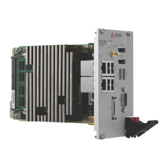
PXIe-3935 1.3 Front Panel I/O & Indicators Figure 1-2: Front Panel Introduction... -
Page 18: Pxie Trigger Connector
The PXIe-3935 provides the following I/O and indicators, as labeled on the front panel. PXI Trigger Connector (SMB jack) 2X DisplayPort Connectors GPIB Connector (Micro D-Sub 25P) Reset Button LED indicators 4X Type-A USB 2.0 ... -
Page 19: Displayport Connectors
PXIe-3935 trigger routing modes from/to the PXIe trigger connector to syn- chronize PXIe modules, including From a selected trigger bus line to PXIe trigger connector From the PXIe trigger connector to a selected trigger bus line From software trigger to a selected trigger bus line ... -
Page 20: Gpib Connector
+V3.3_DDPx_PWR Table 1-1: Display Port Pin Assignment 1.3.3 GPIB Connector The GPIB connector on PXIe-3935 is a micro D-sub 25P connec- tor, controlling external bench-top instruments. Connection to other instruments requires the ACL-IEEE488-MD1-A cable. The on-board GPIB controller provides: ... -
Page 21: Reset Button
Table 1-2: GPIB Pin Description 1.3.4 Reset Button The reset button, activated by insertion of any pin-like implement, executes a hard reset for the PXIe-3935. 1.3.5 LED Indicators Four LED indicators on the front panel indicate operational status of the PXIe-3935, as follows. -
Page 22: Usb 2.0 Ports
1.3.6 USB 2.0 Ports The PXIe-3935 provides four USB 2.0 ports via USB Type A con- nectors on the front panel, all compatible with hi-speed, full-speed and low-speed USB devices. Supported boot devices include USB flash drive, USB floppy, USB CD-ROM, and others, with boot pri- ority and device settings configurable configured in BIOS. -
Page 23: Gigabit Ethernet Ports
PXIe-3935 Signal USB Data- USB Data + Ground Table 1-4: USB 2.0 Port Pin Assignment 1.3.7 Gigabit Ethernet Ports Dual Gigabit Ethernet connection is provided on the PXIe-3935 front panel. 1000Base-T Signal 100/10Base-T Signal MDI0+ MDI0- MDI1+ MDI2+ Reserved MDI2-... -
Page 24: Com Port
The Ethernet ports each include two LED indicators, one Active/ Link indicator and one Speed indicator, functioning as follows. Status Description Ethernet port is disconnected Ethernet port is connected with no Active/Link data transmission (Yellow) Ethernet port is connected with Flashing data transmitted/received 10 Mbps... -
Page 25: Usb 3.0 Ports
Table 1-6: D-Sub 9p COM Port Signal Functions 1.3.9 USB 3.0 Ports The PXIe-3935 provides two Type A USB 3.0 ports on the front panel, supporting SuperSpeed, Hi-Speed, full-speed, and low- speed transmission for downstream. Multiple boot devices, includ- ing USB flash, USB external HD, and USB CD-ROM drives are supported, with boot priority configured in BIOS. -
Page 26: Onboard Connections And Settings
1.3.10 Onboard Connections and Settings Figure 1-6: PXIe-3985 Onboard Configuration SATA Connector Clear CMOS switch System Battery Table 1-7: Onboard Configuration Legend Introduction... -
Page 27: Getting Started
This chapter describes procedures for installing the PXIe-3935 and making preparations for its operation, including hardware and software setup. Please note that the PXIe-3935 is shipped with RAM and HDD or SSD preinstalled. Please contact ADLINK or authorized dealer if there are any problems during the installation. - Page 28 Most operating systems require initial installation from a hard drive, floppy drive, or CD-ROM drive. The PXIe-3935 controller supports USB CD-ROM drive, USB flash disk, USB external hard drive, or a USB floppy drive as the first boot device. See “Boot Setup”...
-
Page 29: Driver Installation
Anti-static wrist strap Anti-static mat ADLINK PXIe-3935 system controllers are electrostatically sensi- tive and can be easily damaged by static electricity. The equip- ment must be handled on a grounded anti-static mat, and operators must wear an anti-static wristband, grounded at the same point as the anti-static mat. - Page 30 Inspect the carton and packaging for damage. Shipping and han- dling may cause damage to the contents. Ensure that all contents are undamaged before installing. All equipment must be protected from static discharge and physical shock. Never remove any of the socketed parts except at a static-free workstation.
-
Page 31: Installing The Pxie-3935
3. Align the controller’s top and bottom edges with the card guides, and carefully slide the PXIe-3935 into the chas- sis, as shown 4. Elevate the latch until the PXIe-3935 is fully seated in the chassis backplane. 5. Fasten the four mounting screws on the front panel of PXIe-3935, and connect all peripheral devices. -
Page 32: Replacing The Hard Drive Or Solid State Drive
2.2.4 Replacing the Hard Drive or Solid State Drive The PXIe-3935 provides a SATA 2.0 port with a pre-installed 2.5" SATA hard drive or solid state drive. Replacing the HDD or SSD is accomplished as follows. 1. Locate the five screws attaching the drive to the bracket on the side of the PXIe-3935. -
Page 33: Replacing The Battery Backup
PXIe-3935 2.2.5 Replacing the Battery Backup The PXIe-3935 is provided with a 3.0 V “coin cell” lithium battery, replacement of which is as follows. 1. Turn off the PXIe chassis. 2. Remove the PXIe-3935 embedded controller from the chassis. Observe all anti-static precautions. -
Page 34: Initiating Backup Bios Flash
BIOS flash on the PXIe-3935 is divided into Backup and Normal sections. In the event of a system malfunction causing the active PXIe-3935 BIOS to crash and then fail to boot, the system auto- matically switches to the secondary backup BIOS. -
Page 35: A Appendix: Pxie Trigger I/O Function Reference
I/O SMB connector on the front panel and the PXIe trigger bus on the backplane. A.1 Data Types The PXIe-3935 library uses these data types in pxitrigio.h in the directory X:\ADLINK\PXIe Trigger IO\Include. It is recommended that you use these data types in your application programs. The table shows the data type names, ranges, and corresponding data types in C/C++, Visual Basic, and Delphi for reference. -
Page 36: Function Library
1.7976831348 floating-point 62315E309 A.2 Function Library This section provides detailed definitions of the functions available in the PXIe-3935 function library. Each function includes a descrip- tion, list of supported cards, syntax, parameter list and Return Code information. A.2.1 TRIG_Init Description Initializes trigger I/O function of PXIe-3935 controller. -
Page 37: Trig_Close
Return Code ERR_NoError ERR_BoardBusy ERR_OpenDriverFail ERR_GetGPIOAddress A.2.2 TRIG_Close Description Closes trigger I/O function of PXIe-3935 controller, releas- ing resources allocated for the trigger I/O function. Users must invoke TRIG_Close before exiting the application. Supported Controllers PXIe-3935, PXI-3980 Syntax C/C++ I16 TRIG_Close() -
Page 38: Trig_Trigger_Route
PXIe trigger bus on the backplane. This function also allows routing of the software- generated trigger signal to SMB connector or trigger bus. Supported Controllers PXIe-3935, PXI-3980 Syntax C/C++ I16 TRIG_Trigger_Route (U32 source, U32 dest,... - Page 39 PXIe-3935 Source of trigger routing. It can be one of the following val- ues. Available value Description PXI_TRIG_VAL_SMB SMB connector on the front panel PXI_TRIG_VAL_SOFT Software-generated trigger signal PXI_TRIG_VAL_TRIG0 PXIe trigger bus #0 PXI_TRIG_VAL_TRIG1 PXIe trigger bus #1 PXI_TRIG_VAL_TRIG2 PXIe trigger bus #2...
-
Page 40: Trig_Trigger_Clear
PXI_TRIG_VAL_TRIG7 PXIe trigger bus #7 Return Code ERR_NoError ERR_BoardNoInit ERR_Set_Path A.2.5 TRIG_Trigger_Clear Description Clears the trigger routing setting Supported Controllers PXIe-3935, PXI-3980 Syntax C/C++ I16 TRIG_Trigger_Clear() Visual Basic TRIG_Trigger_Clear() As Integer Parameters None Return Code ERR_NoError ERR_BoardNoInit PXIe Trigger I/O Function Reference... -
Page 41: Trig_Getsofttrg
PXIe-3935 ERR_Trigger_Clr A.2.6 TRIG_GetSoftTrg Description Acquires the current software trigger state, with default state after system boot of Logic Low Supported Controllers PXIe-3935, PXI-3980 Syntax C/C++ I16 TRIG_GetSoftTrg(U8 *Status) Visual Basic TRIG_GetSoftTrg (status As Byte) As Integer Parameters Status Returns the logic level of software trigger signal... - Page 42 TRIG_Trigger_Route_Query (U32* source, U32* dest, U32* halfway) Visual Basic TRIG_Trigger_Route_Query (source As Long, dest As Long, halfway As Long) As Integer Parameters source Returns to the current source of trigger routing, with possi- ble values including Available Definition Defined Value PXI_TRIG_VAL_NONE PXI_TRIG_VAL_SMB PXI_TRIG_VAL_SOFT...
-
Page 43: Trig_Getdriverrevision
PXI_TRIG_VAL_TRIG1 PXI_TRIG_VAL_TRIG2 PXI_TRIG_VAL_TRIG3 PXI_TRIG_VAL_TRIG4 PXI_TRIG_VAL_TRIG5 PXI_TRIG_VAL_TRIG6 PXI_TRIG_VAL_TRIG7 Return Code ERR_NoError ERR_BoardNoInit ERR_Query_Status A.2.8 TRIG_GetDriverRevision Description Acquires the PXIe Trigger software driver version; format of the version number is major.minor1.minor2 Supported Controllers PXIe-3935, PXI-3980 Syntax C/C++ PXIe Trigger I/O Function Reference... - Page 44 TRIG_GetDriverRevision(unsigned short *major, unsigned short *minor1, unsigned short *minor2) Visual Basic TRIG_GetDriverRevision (major Integer, minor1 As Integer, minor2 As Integer) As Inte- Parameters major Returns the major version number of the PXIe trigger soft- ware driver minor1 Returns the first minor version number of the PXIe trigger software driver minor2 Returns the second minor version number of the PXIe trig-...
-
Page 45: B Appendix: Bios Setup
The Basic Input/Output System (BIOS) provides a basic level of communication between the processor and peripherals. In addition, the BIOS also contains code for various advanced features applied to the PXIe-3935 controller. The BIOS setup program includes menus for configuring settings and enabling PXIe-3935 controller features. -
Page 46: Table B-1: Bios Hot Key Functions
Navigation The BIOS setup/utility uses a key-based navigation system called hot keys. Most BIOS setup utility hot keys can be used at any time during setup navigation, as follows. Key(s) Function Right Arrow, Left Arrow Moves between different setup menus Up Arrow, Down Arrow Moves between options within a setup menu Opens a submenu or displays all available settings... -
Page 47: Main Setup
PXIe-3935 B.2 Main Setup When you first enter the Setup Utility, you will enter the Main setup screen. You can always return to the Main setup screen by select- ing the Main tab. The Main Setup menu provides basic controller information and allows the system time and date to be set, as follows. -
Page 48: Boot Setup
Item Provides USB support and lists devices in USB Configuration USB ports Hardware Health Configuration Displays system voltages and temperatures Onboard Device Configuration Enables/disables LAN and SATA ports Advanced Power Management Shows Watch Dog Timer status Table B-3: BIOS Advanced Setup Menu B.4 Boot Setup Item Boot Configuration... -
Page 49: Save & Exit Setup
PXIe-3935 If passwords are used, the system prompts for a three- to twenty- character password. Typed passwords are not displayed. Item Password Description Administrator Password Sets administrative level password for BIOS User Password Sets user level passwords for BIOS Table B-5: BIOS Security Setup Menu Passwords are not recoverable. - Page 50 The "Restore the default values for all setup options” selection does not restore the original boot priority sequence. You must use the Boot Setup Menu (see “Boot Setup” on page 38) to NOTE: NOTE: manually restore the boot priority sequence. BIOS Setup...
-
Page 51: Important Safety Instructions
PXIe-3935 Important Safety Instructions For user safety, please read and follow all instructions, Warnings, Cautions, and Notes marked in this manual and on the associated device before handling/operating the device, to avoid injury or damage. S'il vous plaît prêter attention stricte à tous les avertissements et mises en garde figurant sur l'appareil , pour éviter des blessures... - Page 52 Never attempt to repair the device, which should only be serviced by qualified technical personnel using suitable tools A Lithium-type battery may be provided for uninterrupted backup or emergency power. Risk of explosion if battery is replaced with one of an incorrect type;...
- Page 53 PXIe-3935 BURN HAZARD Touching this surface could result in bodily injury. To reduce risk, allow the surface to cool before touching. RISQUE DE BRÛLURES Ne touchez pas cette surface, cela pourrait entraîner des blessures. Pour éviter tout danger, laissez la surface refroidir avant de la toucher.
- Page 54 This page intentionally left blank. Important Safety Instructions...
-
Page 55: Getting Service
San Jose, CA 95138, USA Tel: +1-408-360-0200 Toll Free: +1-800-966-5200 (USA only) Fax: +1-408-360-0222 Email: info@adlinktech.com ADLINK Technology (China) Co., Ltd. Address: (201203) 300 Fang Chun Rd., Zhangjiang Hi-Tech Park Pudong New Area, Shanghai, 201203 China Tel: +86-21-5132-8988 Fax: +86-21-5132-3588 Email: market@adlinktech.com... - Page 56 84 Genting Lane #07-02A, Cityneon Design Centre Singapore 349584 Tel: +65-6844-2261 Fax: +65-6844-2263 Email: singapore@adlinktech.com ADLINK Technology Singapore Pte. Ltd. (Indian Liaison Office) Address: #50-56, First Floor, Spearhead Towers Margosa Main Road (between 16th/17th Cross) Malleswaram, Bangalore - 560 055, India Tel: +91-80-65605817, +91-80-42246107 Fax:...
Need help?
Do you have a question about the PXIe-3935 and is the answer not in the manual?
Questions and answers