Table of Contents
Advertisement
Quick Links
We have 45,000 LP502030-PCM-NTC-LD-A02554 - EEMB - Lithium Battery Rectangular 3.7V 250mAh Rechargeable in
stock now. Starting at $0.034. This EEMB part is fully warrantied and traceable.
Looking for a discount?
Check out our current promotions!
This coversheet was created by Verical, a division of Arrow Electronics, Inc. ("Verical"). The attached document was created by the part supplier,
not Verical, and is provided strictly 'as is.' Verical, its subsidiaries, affiliates, employees, and agents make no representations or warranties
regarding the attached document and disclaim any liability for the consequences of relying on the information therein. All referenced brands,
product names, service names, and trademarks are the property of their respective owners.
00000005981LF-000
STM32H753I-EVAL
EOS Power
STMICROELECTRONICS
Buy Now
Buy Now
Give us a call
1-855-837-4225
International: 1-555-555-5555
1-415-281-3866
1-415-281-3866
Arrow Electronics,
Arrow Electronics, Inc
Verical Division
9201 East Dry Creek Road
P.O. Box 740970
Centennial, CO 80112
Los Angeles, CA 90074-0970
Advertisement
Table of Contents

Subscribe to Our Youtube Channel
Related Manuals for ST STM32H753I-EVAL


Summary of Contents for ST STM32H753I-EVAL
- Page 1 We have 45,000 LP502030-PCM-NTC-LD-A02554 - EEMB - Lithium Battery Rectangular 3.7V 250mAh Rechargeable in stock now. Starting at $0.034. This EEMB part is fully warrantied and traceable. 00000005981LF-000 STM32H753I-EVAL EOS Power STMICROELECTRONICS Buy Now Buy Now Looking for a discount?
-
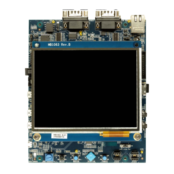
Page 2: Figure 1. Stm32H753I-Eval Evaluation Board (Top View)
UM2199 User manual Evaluation board with STM32H753XI MCU Introduction The STM32H753I-EVAL Evaluation board is a high-end development platform for the ARM ® Cortex ® -M7-based STM32H753XI microcontroller. The STM32H753I-EVAL Evaluation board provides access to all the STM32 peripherals for user applications, and includes an embedded ST-LINK debugger/programmer. -
Page 3: Table Of Contents
8.3.2 ST-LINK/V2-1 firmware upgrade ......13 Power Supply ..........13 Clock source . - Page 4 MEMS microphone coupon connectors CN25 and CN26 ... . 41 Appendix A STM32H753I-EVAL I/O assignment ......42 Appendix B Electrical schematics .
- Page 5 STM32H753I-EVAL I/O assignment ........
- Page 6 Figure 1. STM32H753I-EVAL Evaluation board (top view) ....... . . 1 Figure 2.
-
Page 7: Features
Board expansion connectors: – Extension connectors and memory connectors for daughterboard or wire-wrap board • Flexible power-supply options: ST-LINK USB V or external sources • On-board ST-LINK/V2-1 debugger/programmer with USB re-enumeration capability: mass storage, virtual COM port and debug port •... -
Page 8: Product Marking
Any consequences deriving from such usage will not be at ST charge. In no event, ST will be liable for any customer usage of these engineering sample tools as reference design or in production. -
Page 9: Ordering Information
Ordering information UM2199 Ordering information To order the STM32H753I-EVAL Evaluation board, refer to Table Table 1. Ordering information Order code Target STM32 STM32H753I-EVAL STM32H753XI Delivery recommendations Some verifications are needed before using the Evaluation board for the first time, to make sure that no damage occurred during shipment and that no components are unplugged or lost. -
Page 10: Hardware Layout And Configuration
UM2199 Hardware layout and configuration Hardware layout and configuration The STM32H753I-EVAL Evaluation board is designed around the STM32H753XIH6 (240+25-pin TFBGA package) microcontroller. The hardware block diagram (see Figure illustrates the connection between STM32H753XIH6 and the peripherals (SDRAM, SRAM, NOR Flash, Twin Quad-SPI Flash, color LCD, USB OTG connectors, USART, Ethernet, Audio, FD-CAN, microSD 3.0 card and embedded ST-LINK). -
Page 11: Stm32H753I-Eval Evaluation Board Layout
Hardware layout and configuration UM2199 STM32H753I-EVAL Evaluation board layout Figure 3. STM32H753I-EVAL Evaluation board (top side) 10/69 DocID030512 Rev 1... -
Page 12: Stm32H753I-Eval Evaluation Board Mechanical Drawing
Hardware layout and configuration STM32H753I-EVAL Evaluation board mechanical drawing Figure 4 Table 2 show the mechanical dimensions for the MB1246 board with the 5.7” LCD daughterboard. Figure 4. STM32H753I-EVAL Evaluation board mechanical drawing Table 2. Mechanical dimensions Symbol Size (mm) Symbol Size (mm) -
Page 13: Embedded St_Link/V2-1
® Before connecting the STM32H753I-EVAL Evaluation board to a Windows PC (XP, 7, 8 or 10) through a USB, a driver for the ST-LINK/V2-1 must be installed. It is available at the www.st.com website. In case the STM32H753I-EVAL Evaluation board is connected to the PC before the driver is installed, some STM32H753I-EVAL interfaces may be declared as "unknown"... -
Page 14: St-Link/V2-1 Firmware Upgrade
The ST-LINK/V2-1 embeds a firmware upgrade mechanism for in-situ upgrade through the USB port. As the firmware may evolve during the life time of the ST-LINK/V2-1 product (for example new functionalities, bug fixes, support for new microcontroller families), it is recommended to visit www.st.com... - Page 15 Consequently the board is not powered (LED LD9 remains OFF). Note: In case the STM32H753I-EVAL board is powered by a USB charger, there is no USB enumeration, so the led LD9 remains set to OFF permanently and the board is not powered.
-
Page 16: Table 3. Power Related Jumpers
Default setting: Fitted JP10 is used to select one of the six possible power supply resources. To supply the STM32H753I-EVAL board through the USB connector of the ST- LINK/V2-1 (CN23) set JP10 as shown to the right: (default setting) To supply the STM32H753I-EVAL board through the jack (CN10), set JP10 as... -
Page 17: Clock Source
+3.3 V when JP11 is set as shown to the right: (Default setting) JP11 is connected to the battery when JP11 is set as shown to the right: The LED LD9 lights up when the STM32H753I-EVAL Evaluation board is powered by the 5 V correctly. Note:... -
Page 18: Reset Sources
Note: For Ethernet clock and jumper JP5 configuration refer to Section 8.15. Reset sources The reset signal of STM32H753I-EVAL Evaluation board is low active and the reset sources include: • Reset button B1 • Debugging tools from JTAG/SWD connector CN9 and ETM trace connector CN8 •... -
Page 19: Audio
PDM port of the STM32H753XI, by setting the switch SW2 shown in Table 8. The coupon connectors CN25 and CN26 can be used to support ST-MEMS microphone STEVAL- MKI129V1 after removing SB54 and SB55 solder bridges. 18/69 DocID030512 Rev 1... -
Page 20: Usb Otg1 Fs
SAI_CLK to PG7. USB OTG1 FS The STM32H753I-EVAL Evaluation board supports USB OTG1 full-speed communication through a USB Micro-AB connector (CN18) and USB power switch (U18) connected to . The Evaluation board can be powered by this USB connection at 5 V DC with 500 mA current limitation. -
Page 21: Usb Otg2 Hs And Fs
A green LED LD10 lights up in one of these cases: • Power switch (U18) is ON and the STM32H753I-EVAL board works as a USB host • is powered by another USB host when the STM32H753I-EVAL board works as a USB device. -
Page 22: Microsd Card
8.13 External I C connector The I2C1 bus of the STM32H753XI is connected to CN4 on the STM32H753I-EVAL. The C functional daughterboard can be mounted on the CN4 connector and accessed by the microcontroller through the I2C1 bus. DocID030512 Rev 1... -
Page 23: Fd-Can
UM2199 8.14 FD-CAN The STM32H753I-EVAL Evaluation board supports one channel of the Flexible Data Rate CAN (FD-CAN) communication bus, based on the 3.3 V CAN transceiver. The standby signal on the FD-CAN transceiver is controlled by PD3 of the STM32H753XI. -
Page 24: Twin Quad-Spi Nor Flash
UM2199 Hardware layout and configuration A 128-Mbit NOR Flash is connected to the NOR/PSRAM1 bank1 of the FMC interface. The 16-bit operation mode is selected by pull-up resistor connected to the BYTE pin of NOR Flash. The write protection can be enabled or disabled, depending on how the jumper JP13 is set, as showed in Table Table 13. -
Page 25: Table 14. Lcd Module Connector (Cn20)
Hardware layout and configuration UM2199 The 4-direction joystick (B4) with selection, Wakeup (B2) and Tamper/key button (B3) are available as input devices. 5.7” 640x480 TFT color LCD with capacitive touch panel is connected to the RGB LCD interface of the STM32H753XI microcontroller. Table 14. -
Page 26: Mfx (Multi Function Expander)
Figure 6. Orientation setting of 5.7-inch LCD daughterboard 8.20 MFX (Multi Function eXpander) MFX circuit on STM32H753I-EVAL Evaluation board acts as IO-expander. The communication interface between MFX and STM32H753XI is I2C1 bus. The signals connected to MFX are listed in Table Table 15. -
Page 27: Connectors
Connectors UM2199 Connectors Ethernet RJ45 connector CN1 Figure 7. Ethernet RJ45 connector CN1 (front view) Table 16. RJ45 connector CN1 Pin number Description Description number TxData+ TxData- RxData+ Shield Shield RxData- Shield Shield RS232 connector CN2 Figure 8. RS232 connector CN2 (front view) Table 17. -
Page 28: Can D-Type, 9-Pin Male Connector Cn3
UM2199 Connectors Table 17. RS232 connector CN2 with ISP support (continued) Pin number Description Description number RS232_TX (PB14) Bootloader_RESET CAN D-type, 9-pin male connector CN3 Figure 9. CAN D-type, 9-pin connector CN3 (front view) Table 18. CAN D-type 9-pin male connector CN3 Pin number Description Pin number... -
Page 29: Analog Input-Output Connector Cn5
Daughterboard extension connector CN6 and CN7 Two 60-pin male headers CN6 and CN7 can be used to connect a daughterboard or a standard wrapping board to the STM32H753I-EVAL Evaluation board. All GPI/Os are available on CN6 and CN7 and memory connectors on CN11 and CN12. -
Page 30: Table 21. Daughterboard Extension Connector Cn6
UM2199 Connectors Table 21. Daughterboard extension connector CN6 How to disconnect with function block on Description Alternative function STM32H753I-EVAL board ULPI_STP Remove R124 OSC_IN Remove R15, Close SB39 RESET# PI11 ULPI_DIR Remove R123 ULPI_D7 Remove R101 QSPI_BK1_IO0 Remove R38 PG14... -
Page 31: Table 22. Daughterboard Extension Connector Cn7
Connectors UM2199 Table 21. Daughterboard extension connector CN6 (continued) How to disconnect with function block on Description Alternative function STM32H753I-EVAL board PC2_C PC3_C PA0_C Potentiometer Open SB43 PA1_C ULPI_CK Remove R118 QSPI_CLK ULPI_NXT Remove R117 RMII_RXD1 Remove R39 QSPI_BK2_IO2 Remove R33... - Page 32 UM2199 Connectors Table 22. Daughterboard extension connector CN7 (continued) How to disconnect with function block on Description Alternative function STM32H753I-EVAL board PC13 KEY_TAMP_1/WKUP2 Remove R193 SDIO_1_CKIN RGB_LCD_DE Disconnect CN20 JTDO/TRACESWO Remove R60 RGB_LCD_B7 Remove R199, Disconnect CN20 RGB_LCD_B5 Remove R201, Disconnect CN20...
- Page 33 Connectors UM2199 Table 22. Daughterboard extension connector CN7 (continued) How to disconnect with function block on Description Alternative function STM32H753I-EVAL board Remove R160, R181, R209, Disconnect I2C_1_SDA CN4, CN15, CN20 Remove R155, R180, R212, Disconnect I2C_1_SCL CN4, CN15, CN20 NJTRST...
-
Page 34: Etm Trace Debugging Connector Cn8
UM2199 Connectors ETM trace debugging connector CN8 Figure 12. ETM trace debugging connector CN8 (top view) Table 23. ETM Trace debugging connector CN8 Pin number Description Description number +3.3V TMS/PA13 TCK/PA14 TDO/PB3 TDI/PA15 RESET# TraceCLK/PE2 TraceD0/PE3 or SWO/PB3 TraceD1/PE4 or nTRST/PB4 TraceD2/PE5 TraceD3/PE6 JTAG/SWD connector CN9... -
Page 35: Power Connector Cn10
TDO/SWO(PB3) RESET# DBGRQ(PJ7) DBGACK(PJ12) Power connector CN10 STM32H753I-EVAL Evaluation board can be powered from a DC 5 V power supply through the external power supply jack (CN10) shown in Figure 14. The central pin of CN10 must be positive. Figure 14. Power supply connector CN10 (front view) 9.10... -
Page 36: Table 25. Memory Connector Cn11
UM2199 Connectors Table 25. Memory connector CN11 How to disconnect with function block on Description Alternative function STM32H753I-EVAL board SDNE1 PF13 PF12 PE10 PE12 PE15 PE13 PD11 PD12 A15/BA1 PH11 PD13 PD14 SDNWE PF14 PF11 SDNRAS PE11 PF15 PE14 PH10... -
Page 37: Table 26. Memory Connector Cn12
Connectors UM2199 Table 25. Memory connector CN11 (continued) How to disconnect with function block on Description Alternative function STM32H753I-EVAL board PH12 PD10 PD15 SDCLK Table 26. Memory connector CN12 How to disconnect with function block on Description Alternative function STM32H753I-EVAL board... -
Page 38: Microsd Connector Cn13
UM2199 Connectors Table 26. Memory connector CN12 (continued) How to disconnect with function block on Description Alternative function STM32H753I-EVAL board A23/PDM1_CK1/ Open SB11, SB15, SB57 SAI1_MCLK_A /TRACECLK PH15 PH14 +3.3V 9.11 microSD connector CN13 Figure 15. microSD connector (top view) -
Page 39: Usb Otg2 Hs Micro-Ab Connector Cn14
Connectors UM2199 Table 27. microSD connector CN13 Description Description number number SD_DATA2 Vss/GND SD_DATA3 SD_DATA0 SD_CMD SD_DATA1 +2.9V_SD MicroSDcard_detect SD_CLK (MFX GPIO15) 9.12 USB OTG2 HS Micro-AB connector CN14 Figure 16. USB OTG HS Micro-AB connector CN14 (front view) Table 28. USB OTG HS Micro-AB connector CN14 Pin number Description Pin number... -
Page 40: Usb Otg2 Fs Micro-Ab Connector Cn16
UM2199 Connectors 9.13 USB OTG2 FS Micro-AB connector CN16 Figure 17. USB OTG FS Micro-AB connector CN16 (front view) Table 29. USB OTG1 FS Micro-AB connector CN18 Pin number Description Pin number Description VBUS (PB13) ID (PB12) D- (PB14) D+ (PB15) 9.14 USB OTG1 FS Micro-AB connector CN18 Figure 18. -
Page 41: Audio Jack Cn17
Connectors UM2199 9.15 Audio jack CN17 A 3.5 mm stereo audio jack CN17 is available on STM32H753I-EVAL Evaluation board to support headset (headphone and microphone integrated). 9.16 Audio jack (speaker) CN19 A 3.5mm stereo audio jack CN19 for speaker out is available on STM32H753I-EVAL Evaluation board to support an external speaker. -
Page 42: Mems Microphone Coupon Connectors Cn25 And Cn26
UM2199 Connectors Table 31. USB Micro-B connector CN23 (front view) Pin number Description Pin number Description (power) 9.21 MEMS microphone coupon connectors CN25 and CN26 Figure 20. MEMS microphone coupon connectors CN25 and CN26 (top view) Table 32. 2.21 MEMS microphone coupon connectors CN25 and CN26 Pin number Description Pin number... -
Page 43: Appendix A Stm32H753I-Eval I/O Assignment
STM32H753I-EVAL I/O assignment UM2199 Appendix A STM32H753I-EVAL I/O assignment Table 33. STM32H753I-EVAL I/O assignment Pin No. Pin Name Default function Alternative function PA0-WKUP KEY_WKUP0 RMII_REF_CLK RMII_MDIO ULPI_D0 EXT_RESET/LED3 ULPI_CK GPIO_LCD_BACKLIGHT_CTRL RMII_CRS_DV MCO1 USB_FS1_VBUS PA10 USB_FS1_ID PA11 USB_FS1_DM FDCAN_1_RXFD PA12 USB_FS1_DP... - Page 44 UM2199 STM32H753I-EVAL I/O assignment Table 33. STM32H753I-EVAL I/O assignment (continued) Pin No. Pin Name Default function Alternative function ULPI_STP RMII_MDC PDM1_D1 DFSDM_CKOUT DFSDM_DATA1 RMII_RXD0 RMII_RXD1 SDIO_1_D0DIR SDIO_1_D123DIR SDIO_1_D0 SDIO_1_D1 PC10 SDIO_1_D2 PC11 SDIO_1_D3 PC12 SDIO_1_CK PC13- KEY_TAMP_1/WKUP2 ANTI_TAMP PC14- OSC32_IN...
- Page 45 STM32H753I-EVAL I/O assignment UM2199 Table 33. STM32H753I-EVAL I/O assignment (continued) Pin No. Pin Name Default function Alternative function FMC_NBL1 FMC_A23/TRACECLK/ PDM1_CK1 SAI_1_MCLK_A SAI1_SD_B FMC_A19/TRACED0 SAI1_FS_A FMC_A20/TRACED1 SAI1_SCK_A FMC_A21/TRACED2 SAI1_SD_A FMC_A22/TRACED3 FMC_D4 FMC_D5 FMC_D6 PE10 FMC_D7 PE11 FMC_D8 PE12 FMC_D9 PE13...
- Page 46 UM2199 STM32H753I-EVAL I/O assignment Table 33. STM32H753I-EVAL I/O assignment (continued) Pin No. Pin Name Default function Alternative function FMC_A13 FMC_A14 / SDR_BA0 FMC_A15 / SDR_BA1 QSPI_BK1_NCS SAI_1_MCLK_A SDR_SDCLK QSPI_BK2_IO2 PG10 FMC_NE3 PG11 RMII_TX_EN PG12 RMII_TXD1 PG13 RMII_TXD0 PG14 QSPI_BK2_IO3 PG15...
- Page 47 STM32H753I-EVAL I/O assignment UM2199 Table 33. STM32H753I-EVAL I/O assignment (continued) Pin No. Pin Name Default function Alternative function FMC_NBL3 FMC_D28 FMC_D29 PI8- ANTI GPIO_EXPANDER_INT TAMP2 FMC_D30 PI10 FMC_D31 PI11 ULPI_DIR PI12 RGB_LCD_HSYNC PI13 RGB_LCD_VSYNC PI14 RGB_LCD_CLK PI15 RGB_LCD_R0 RGB_LCD_R1 RGB_LCD_R2...
- Page 48 UM2199 STM32H753I-EVAL I/O assignment Table 33. STM32H753I-EVAL I/O assignment (continued) Pin No. Pin Name Default function Alternative function RGB_LCD_DE PA0_C Potentiometer PA1_C PC2_C PC3_C DocID030512 Rev 1 47/69...
-
Page 49: Appendix B Electrical Schematics
Electrical schematics UM2199 Appendix B Electrical schematics This section provides the design schematics for the STM32H753I-EVAL Evaluation board: • Overall schematics for the STM32H753I-EVAL, see Figure 21 • STM32H753I-EVAL MCU, see Figure 22 • Power, see Figure 23 • SRAM, Flash and SDRAM, see Figure 24 •... -
Page 50: Figure 21. Stm32H753I-Eval Evaluation Board
Figure 21. STM32H753I-EVAL Evaluation board U_MCU U_Memory MCU.SchDoc Same length Memory.SchDoc R212 +3V3 I2C1_SCL A[0..23] A[0..23] R209 I2C1_SDA D[0..31] D[0..31] U_Audio 90MHz clock SDCLK SDCLK Audio.SchDoc SDNE1 SDNE1 I2C1_SCL SAI1_SCKA SAI1_SCKA SDNRAS SDNRAS I2C1_SDA SAI1_FSA SAI1_FSA SDNCAS SDNCAS SAI1_SDA SAI1_SDA... -
Page 51: Figure 22. Stm32H753I-Eval Mcu
Figure 22. STM32H753I-EVAL MCU R265 R256 WAKEUP R262 R264 RMII_REF_CLK R270 R263 ETH_MDIO SDIO1_CMD ULPI_D0 R260 R267 LED3_RGB FDCAN1_STBY R261 EXT_RESET FMC_NOE FMC_NBL2 R272 ULPI_CK FMC_NWE FMC_NBL3 R259 R243 LCD_BL_CTRL FMC_NWAIT QSPI_BK1_NCS SAI1_MCLKA SB56 Open R240 RMII_CRS_DV FMC_NE1 R268 SDCLK... -
Page 52: Figure 23. Power
Figure 23. Power VDD_MCU ZEN056V130A24LS CN10 220uF DC-10B SMAJ5.0A-TR 100nF BNX002-01 Reserved for other use VDD_MCU JP10 BEAD(FCM1608KF-601T03) VBUS_HS VBUS_FS1 VBUS_FS2 +3V3 VDD_MCU R159 U5V_ST_LINK 11 12 4.7uF VDD_SDC Header 6X2 2.2uH(LQM2MPN2R2NG0) SB10 Open [N/A] SB16 Open +3V3 TP11 10uF SB20 Open LD1086D2M33... -
Page 53: Figure 24. Sram, Flash And Sdram
Figure 24. SRAM, FLASH and SDRAM D[0..31] D[0..31] A[0..23] A[0..23] DQ31 DQ30 I/O15 DQ15A-1 DQ29 I/O14 DQ14 DQ28 I/O13 DQ13 DQ27 I/O12 DQ12 DQ26 I/O11 DQ11 DQ25 I/O10 DQ10 DQ24 I/O9 DQ23 I/O8 DQ22 I/O7 DQ21 I/O6 DQ20 I/O5 DQ19 I/O4 DQ18 I/O3... -
Page 54: Figure 25. Audio
Figure 25. Audio +3V3 LDO1VDD AGND Default I2C Address:0011010 +3V3 AVDD1 AGND SPKVDD1 AGND +1V8 SPKVDD2 SPKGND1 AVDD2 SPKGND2 +1V8 CPVDD CPGND +3V3 DCVDD DGND DBVDD HP2GND +1V8 LDO2VDD R160 I2C1_SDA R157 R155 +3V3 LDO1ENA SCLK I2C1_SCL R163 [N/A] LDO2ENA CS/ADDR +3V3 VREFC... -
Page 55: Figure 26. Lcd Connectors
Figure 26. LCD connectors Extension connector (Reserved for other use) LCD Connector CN15 TOUCH_INT DSI_CK_P DSI_CK_N DSI_D2_P SB34 Closed DSI_D2_N SB33 Closed DSI_D0_P DSI_D0_N DSI_D3_P SB32 Closed DSI_D3_N SB31 Closed DSI_D1_P DSI_D1_N C147 BEAD(FCM1608KF-601T03) C148 10uF 100nF CN20 BEAD(FCM1608KF-601T03) LCD_R[0..7] PI15 LCD_R0 LCD_G0... -
Page 56: Figure 27. Ethernet
Figure 27. Ethernet +3V3 BEAD 100nF +3V3 I/O1 I/O4 Vbus I/O2 I/O3 C102 USBLC6-4SC6 100nF Diff Pair 100ohm TD_P Diff Pair 100ohm PG11 TD_N RMII_TX_EN TXEN PG13 RMII_TXD0 TXD0 PG12 RD_P RMII_TXD1 TXD1 RD_N RMII_RXD0 RXD0/MODE0 Diff Pair 100ohm RMII_RXD1 RXD1/MODE1 LED1/nINT/nPME/REGOFF Diff Pair 100ohm... -
Page 57: Figure 28. Usb Otg Hs
Figure 28. USB OTG HS +3V3 R289 CN16 PB13 VBUS_FS2 VBUS PB14 USB_FS2_DM PB15 USB_FS2_DP PB12 USB_FS2_ID Green Shield Shield R135 ESDA6V1BC6 Shield 9013 Shield 475900001 R137 +3V3 R126 MFX_GPIO8 R287 OTG_FS2_OverCurrent SB28 +3V3 To MFX R125 MFX_GPIO9 SB29 Open Open OTG_FS2_PowerSwitchOn R127... -
Page 58: Figure 29. Usb Otg Fs
Figure 29. USB OTG FS +3V3 R290 MFX_GPIO6 OTG_FS1_OverCurrent R144 To MFX R146 CN18 FAULT VBUS MFX_GPIO7 R141 OTG_FS1_PowerSwitchOn From MFX STMPS2151STR 4.7uF R140 Shield Shield Shield Shield 475900001 +3V3 VBUS_FS1 PA11 USB_FS1_DM PA12 USB_FS1_DP PA10 R165 USB_FS1_ID ESDA6V1BC6 LD10 Green R153 9013... - Page 59 Figure 30. RS232 +3V3 C104 C101 100nF 100nF DB9-male USART1 C105 100nF 100nF 100nF T1IN T1OUT PB14 RS232_TX T2IN T2OUT T3IN T3OUT R1OUTB Bootloader_BOOT0 R2OUTB R1OUT R1IN R2OUT R2IN PB15 RS232_RX R3OUT R3IN Bootloader_RESET R4OUT R4IN R5OUT R5IN +3V3 nSHDN ST3241EBPR RS232 Title:...
-
Page 60: Figure 31. Fdcan And Qspi
Figure 31. FDCAN and QSPI FDCAN C100 FDCAN1_STBY DB9-male CAN connector Default setting: Open 100nF PA12 FDCAN1_TX STBY CANH CANL PA11 FDCAN1_RX +3V3 MCP2562FD 100nF ESDCAN02-2BWY R213 R214 [N/A] +3V3 Twin Quad SPI Flash QSPI_CLK BK2_IO3 QSPI_CLK QSPI_BK1_IO3 HOLD_1#/DQ3 CLK_1 QSPI_CLK HOLD#/DQ3 R225... -
Page 61: Figure 32. Microsd 3.0 Card
Figure 32. microSD 3.0 card MICRO SD 3.0 Card +3V3 R112 R115 R110 [N/A] [N/A] [N/A] [N/A] [N/A] +2V9_SD Module board PC12 SDIO1_CLK CLK_IN DATA0_SD SDIO1_CKIN CLK_FB DATA1_SD DATA2_SD SDIO1_CMD CMD_H DATA3_SD SDIO1_CDIR DIR_CMD CLK_SD CMD_SD SDIO1_D0 DATA0_H SDIO1_D1 DATA1_H PC10 SDIO1_D2 DATA2_H... -
Page 62: Figure 33. Peripherals
Figure 33. Peripherals Buttons Potentiometer +3V3 +3V3 R205 R194 Two pin header for external analog input +3V3 R193 PC13 TAMPER_KEY WKUP [N/A] PA0_C Potentiometer 100nF R11 0 USER (Blue) 3386P-103(10K) R203 100nF WAKEUP [N/A] R204 R192 220K Close to MCU on PCB Wakeup Button Tamper &... -
Page 63: Figure 34. Extension Connectors
Figure 34. Extension connectors Place close Memory CN11 SDNE1 SDNWE PF13 PF14 PF12 PF11 SDNRAS SB39 Left Right Open PF10 11 12 PE10 SB40 PC15 PC14 13 14 R215 Open PI14 PI12 Open PE12 PE11 RESET# 15 16 PI11 Open PI13 PE15 PF15... -
Page 64: Figure 35. St-Link/V2-1
Figure 35. ST-LINK/V2-1 VBUS_HS +3V3_ST_LINK BAT60JFILM R292 R293 VBUS_FS1 BAT60JFILM LDK120M33R +3V3_ST_LINK BAT60JFILM C162 C165 C166 JP15 VBUS_FS2 Vout 100nF 100nF 100nF 100nF +3V3_ST_LINK BAT60JFILM BYPASS R176 1uF_X5R_0603 1uF_X5R_0603 BAT60JFILM 100K +3V3_ST_LINK 100nF 10nF_X7R_0603 100nF BAT60JFILM Board Ident: PC13=0 VUSB_ST_LINK... -
Page 65: Figure 36. Mfx
Figure 36. MFX Multi Function eXpander +3V3 +3V3 +3V3 one capacitor close to each MFX pins: VDD, VDD_1, VDD_2, VDD_3 Ferrite C169 C167 C171 C168 C163 100nF 100nF 100nF 100nF 100nF 100nF +3V3 R172 STM32L152CCT6 GPIO0 MFX_IO0 Loop SPARE GPIO1 MFX_IO1 CN22 TP10... -
Page 66: Figure 37. Jtag And Trace
Figure 37. JTAG and trace +3V3 [N/A] [N/A] [N/A] [N/A] PA13 TMS/SWDIO PA14 TCK/SWCLK TDO/SWO PA15 TRST RESET# [N/A] Trace connector JTAG connector +3V3 JTAG +3V3 +3V3 [N/A] [N/A] [N/A] SB24 Open DBGRQ SB25 Open PJ12 DBGACK P127B-2*10MGF-079-1E7A FTSH-110-01-L-DV (Samtec) TRACE_D3 TRACE_D2 TRACE_D1... -
Page 67: Figure 38. 5.7" Lcd Board
Figure 38. 5.7” LCD board [N/A] BLGND DCLK HSYNC HSYNC VSYNC VSYNC [N/A] BL_CTRL 11 12 13 14 VLED 15 16 BLVDD VLED 17 18 VLED 19 20 21 22 4.7uF 23 24 100nF 100nF 100nF HSYNC 25 26 VSYNC 4.7uF 27 28 100nF... -
Page 68: Appendix C Board Revision History And Limitations
Board revision history and limitations Appendix C Board revision history and limitations Table 34. Board revision history and limitations Board Version Revision details Known limitations MB1246 (Main board) B-01 Initial version for STM32H753I-EVAL MB1065 (LCD board) B-01 Initial version DocID030512 Rev 1 67/69... -
Page 69: Revision History
Revision history UM2199 Revision history Table 35. Document revision history Date Revision Changes 29-Jun-2017 Initial release. 68/69 DocID030512 Rev 1... - Page 70 ST products and/or to this document at any time without notice. Purchasers should obtain the latest relevant information on ST products before placing orders. ST products are sold pursuant to ST’s terms and conditions of sale in place at the time of order acknowledgement.
Need help?
Do you have a question about the STM32H753I-EVAL and is the answer not in the manual?
Questions and answers