Table of Contents
Advertisement
Quick Links
We have 45,000 LP502030-PCM-NTC-LD-A02554 - EEMB - Lithium Battery Rectangular 3.7V 250mAh Rechargeable in
stock now. Starting at $0.034. This EEMB part is fully warrantied and traceable.
Looking for a discount?
Check out our current promotions!
This coversheet was created by Verical, a division of Arrow Electronics, Inc. ("Verical"). The attached document was created by the part supplier,
not Verical, and is provided strictly 'as is.' Verical, its subsidiaries, affiliates, employees, and agents make no representations or warranties
regarding the attached document and disclaim any liability for the consequences of relying on the information therein. All referenced brands,
product names, service names, and trademarks are the property of their respective owners.
00000005981LF-000
HSC-ADC-EVALCZ
EOS Power
ANALOG DEVICES
Buy Now
Buy Now
Give us a call
1-855-837-4225
International: 1-555-555-5555
1-415-281-3866
1-415-281-3866
Arrow Electronics,
Arrow Electronics, Inc
Verical Division
9201 East Dry Creek Road
P.O. Box 740970
Centennial, CO 80112
Los Angeles, CA 90074-0970
Advertisement
Table of Contents

Related Manuals for Analog Devices AD9642


Summary of Contents for Analog Devices AD9642
- Page 1 We have 45,000 LP502030-PCM-NTC-LD-A02554 - EEMB - Lithium Battery Rectangular 3.7V 250mAh Rechargeable in stock now. Starting at $0.034. This EEMB part is fully warrantied and traceable. 00000005981LF-000 HSC-ADC-EVALCZ EOS Power ANALOG DEVICES Buy Now Buy Now Looking for a discount? Check out our current promotions!
-
Page 2: Features
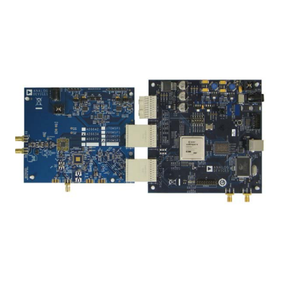
GENERAL DESCRIPTION Analog signal source and antialiasing filter Sample clock source (if not using the on-board oscillator) This user guide describes the AD9642, AD9634, and AD6672 evaluation board, which provides all of the support circuitry 2 switching power supplies (6.0 V, 2.5 A), CUI... -
Page 3: Table Of Contents
UG-386 AD9642/AD9634/AD6672 User Guide TABLE OF CONTENTS Features ....................1 Output Signals ................4 Equipment Needed ................1 Default Operation and Jumper Selection Settings ....4 Software Needed ................1 Evaluation Board Software Quick Start Procedures .....6 Documents Needed ................1 Configuring the Board ..............6 General Description ................. -
Page 4: Evaluation Board Hardware
LDOs. This enables the performance of the AD9642, AD9634, or AD6672. It is critical user to bias each section of the board individually. Use P202 that the signal sources used for the analog input and the clock and P203 to connect a different supply for each section. -
Page 5: Output Signals
Analog Devices evaluation boards can accept ~2.8 V p-p or 13 dBm sine wave input for the clock. Clock Circuitry The default clock input circuit that is populated on the AD9642/ OUTPUT SIGNALS AD9634/AD6672 evaluation board uses a simple transformer-... - Page 6 AD9642/AD9634/AD6672 User Guide UG-386 Switching Power Supply Install L201 and L202. Remove JP201 and JP203. Optionally, the ADC on the board can be configured to use the Remove jumpers from across Pin 1 and Pin 2 on P107 and ADP2114 dual switching power supply to provide power to the P108, respectively.
-
Page 7: Evaluation Board Software Quick Start Procedures
UG-386 AD9642/AD9634/AD6672 User Guide EVALUATION BOARD SOFTWARE QUICK START PROCEDURES This section provides quick start procedures for using the AD9642/ AD9634/AD6672 evaluation board. Both the default and optional settings are described. CONFIGURING THE BOARD Before using the software for testing, configure the evaluation... - Page 8 AD9642/AD9634/AD6672 User Guide UG-386 Figure 7. VisualAnalog, Main Window Setting Up the SPI Controller Software After the ADC data capture board setup is complete, set up the SPI controller software using the following procedure: Open the SPI controller software by going to the Start menu or by double-clicking the SPIController software desktop icon.
- Page 9 UG-386 AD9642/AD9634/AD6672 User Guide Click the New DUT button in the SPIController window In the ADCBase 0 tab of the SPIController window, find the (see Figure 9). CLK DIV(B) section (see Figure 10). If using the clock divider, use the drop-down box to select the correct clock divide ratio, if necessary.
- Page 10 AD9642/AD9634/AD6672 User Guide UG-386 Figure 11. SPI Controller, Example ADCBase 0 Tab—NSR Settings for the AD6672 If using the noise shaping requantizer (NSR) feature of the Click the Run button in the VisualAnalog toolbar (see AD6672, the settings in the ADCBase 0 tab must be Figure 12).
- Page 11 Click the Save disk icon within the Graph window to save the performance plot data as a .csv formatted file. See –120 Figure 13 for an example. –140 FREQUENCY (MHz) Figure 13. Typical FFT, AD9642 Figure 14. Graph Window of VisualAnalog (AD9642) Rev. A | Page 10 of 26...
- Page 12 AD9642/AD9634/AD6672 User Guide UG-386 If operating the AD6672 with NSR enabled, certain options in the FFT Analysis box (see Figure 15) in VisualAnalog to in VisualAnalog must be enabled. Click the button circled bring up the options for setting the NSR.
- Page 13 UG-386 AD9642/AD9634/AD6672 User Guide Troubleshooting Tips Configure the settings in the FFT analysis to match the If the FFT plot appears abnormal, do the following: settings selected for the NSR in the SPI controller (see Figure 16). If you see a normal noise floor when you disconnect the signal generator from the analog input, be sure that you are not overdriving the ADC.
-
Page 14: Evaluation Board Schematics And Artwork
AD9642/AD9634/AD6672 User Guide UG-386 EVALUATION BOARD SCHEMATICS AND ARTWORK Figure 18. Device Under Test and Related Circuits Rev. A | Page 13 of 26... - Page 15 UG-386 AD9642/AD9634/AD6672 User Guide Figure 19. Board Power Input and Supply Rev. A | Page 14 of 26...
- Page 16 AD9642/AD9634/AD6672 User Guide UG-386 Figure 20. Passive Analog Input Circuits Rev. A | Page 15 of 26...
- Page 17 UG-386 AD9642/AD9634/AD6672 User Guide Figure 21. Optional Active Input Circuits Rev. A | Page 16 of 26...
- Page 18 AD9642/AD9634/AD6672 User Guide UG-386 Figure 22. Default and Optional Clock Input Circuits Rev. A | Page 17 of 26...
- Page 19 UG-386 AD9642/AD9634/AD6672 User Guide FAST_SPI_EN DRVDD DRVDD R603 C601 1.1K 0.1UF 3P3V_DIGITAL DRVDD U603 R605 TP_DUT_SDIO ADG734BRUZ R626 3P3V_DIGITAL U601 1.1K 1.1K NC7WZ07P6X FPGA_SDIO CYP_SDI DUT_SDIO CYP_SDO R608 KP_VDDIO R606 C602 TP_CYP_SDIO LAYOUT: PLACE C602 NEAR DUT 0.1UF CYP_SDIO NOTE: THIS SYMBOL IS DRAWN GIVEN INPUT 1 LOGIC...
- Page 20 AD9642/AD9634/AD6672 User Guide UG-386 Figure 24. Top Side Figure 25. Ground Plane (Layer 2) Rev. A | Page 19 of 26...
- Page 21 UG-386 AD9642/AD9634/AD6672 User Guide Figure 26. Power Plane (Layer 3) Figure 27. Power Plane (Layer 4) Rev. A | Page 20 of 26...
- Page 22 AD9642/AD9634/AD6672 User Guide UG-386 Figure 28. Ground Plane (Layer 5) Figure 29. Bottom Side Rev. A | Page 21 of 26...
-
Page 23: Ordering Information
UG-386 AD9642/AD9634/AD6672 User Guide ORDERING INFORMATION BILL OF MATERIALS Table 1. AD9642/AD9634/AD6672 Bill of Materials Item Reference Designator Description Manufacturer/Part No. AD9642EE01A Printed circuit board, AD9642 engineering board C101, C103, C105, C109 to C113, 0.1 µF capacitor ceramic X5R 0201... - Page 24 AD9642/AD9634/AD6672 User Guide UG-386 Item Reference Designator Description Manufacturer/Part No. P601, P602 6469169-1 CONN_PCB 60PIN RA connector TYCO 6469169-1 R201 261 resistor film chip thick NIC COMP CORP NRC06F2610TRF R205, R222 1.00 kΩ resistor precision thick film chip Panasonic ERJ-2RKF1001X...
-
Page 25: Related Links
UG-386 AD9642/AD9634/AD6672 User Guide Item Reference Designator Description Manufacturer/Part No. C314, C406 to C408, C529, C603 0.1 µF capacitor ceramic X7R 0402 Murata GRM155R71C104KA88D C409, C410 5 pF capacitor Panasonic ECU-E1H050CCQ C522 390 pF capacitor ceramic C0G 0402 Murata GRM1555C1H391JA01D... - Page 26 AD9642/AD9634/AD6672 User Guide UG-386 NOTES Rev. A | Page 25 of 26...
- Page 27 By using the evaluation board discussed herein (together with any tools, components documentation or support materials, the “Evaluation Board”), you are agreeing to be bound by the terms and conditions set forth below (“Agreement”) unless you have purchased the Evaluation Board, in which case the Analog Devices Standard Terms and Conditions of Sale shall govern. Do not use the Evaluation Board until you have read and agreed to the Agreement.
Need help?
Do you have a question about the AD9642 and is the answer not in the manual?
Questions and answers