Table of Contents
Advertisement
Quick Links
Advertisement
Table of Contents

Related Manuals for Teridian 71M6513


Summary of Contents for Teridian 71M6513
- Page 1 71M6513/71M6513H Demo Board USER’S MANUAL 4/9/2007 10:06 AM Revision 5.6 TERIDIAN Semiconductor Corporation 6440 Oak Canyon Rd. Irvine, CA 92618-5201 Phone: (714) 508-8800 ▪ Fax: (714) 508-8878 http://www.teridian.com/ meter.support@teridian.com Downloaded from: http://www.datasheetcatalog.com/...
- Page 2 71M6513/71M6513H Demo Board User’s Manual TERIDIAN Semiconductor Corporation makes no warranty for the use of its products, other than expressly contained in the Company’s warranty detailed in the TERIDIAN Semiconductor Corporation standard Terms and Conditions. The company assumes no responsibility for any errors which may appear in this document, reserves the right to change devices or specifications detailed herein at any time without notice and does not make any commitment to update the information contained herein.
- Page 3 71M6513/71M6513H Demo Board User’s Manual 71M6513/71M6513H 3-Phase Energy Meter IC DEMO BOARD USER’S MANUAL Page: 3 of 112 Revision 5.6 © 2005-2006 TERIDIAN Semiconductor Corporation Downloaded from: http://www.datasheetcatalog.com/...
-
Page 4: Table Of Contents
Updating Calibration Data in Flash Memory without Using the ICE or a Programmer........29 1.9.5 Automatic Gains Calibration .......................... 30 1.9.6 Loading the 6513_demo.hex file into the Demo Board.................. 30 1.9.7 The Programming Interface of the 71M6513/6513H ..................32 1.10 Demo Code..............................33 1.10.1 Demo Code Description..........................33 1.10.2 Demo Code MPU Parameters ........................ - Page 5 Figure 1-2: Block diagram for the TERIDIAN D6513T3B2 Demonstration Meter with Debug Board......... 12 Figure 1-3: Block diagram for the TERIDIAN D6513T3C1 and D6513T3D2 Demo Boards with Debug Board ....13 Figure 1-4: Hyperterminal Sample Window with Disconnect Button (Arrow) ..............15 Figure 1-5: Port Speed and Handshake Setup (left) and Port Bit setup (right)..............
- Page 6 Figure 4-11: TERIDIAN D6513T3B2 Demo Board: Bottom View ..................91 Figure 4-12: TERIDIAN D6513T3B2 Demo Board: Top Signal Layer ................92 Figure 4-13: TERIDIAN D6513T3B2 Demo Board: Middle Layer 1 (Ground Plane) ............93 Figure 4-14: TERIDIAN D6513T3B2 Demo Board: Middle Layer 2 (Supply Plane) ............94 Figure 4-15: TERIDIAN D6513T3B2 Demo Board: Bottom Signal Layer ................
- Page 7 Figure 4-30: Debug Board: Middle Layer 2 (Supply Plane) ..................... 109 Figure 4-31: Debug Board: Bottom Trace Layer ......................109 Figure 4-32: TERIDIAN 71M6513/71M6513H epLQFP100: Pinout (top view) ..............112 List of Tables Table 1-1: Jumper settings on Debug Board........................14 Table 1-2: Straight cable connections ..........................
- Page 8 71M6513/71M6513H Demo Board User’s Manual Page: 8 of 112 Revision 5.6 © 2005-2006 TERIDIAN Semiconductor Corporation Downloaded from: http://www.datasheetcatalog.com/...
-
Page 9: Getting Started
Debug Board that allows a connection to a PC through a RS232 port. The demo board allows the evaluation of the 71M6513 or 71M6513H energy meter chip for measurement accuracy and overall system use. -
Page 10: Demo Kit Contents
71M6513/71M6513H Demo Board User’s Manual DEMO KIT CONTENTS • Demo Board with 71M6513/71M6513H IC and pre-loaded demo program: • D6513T3B2 Demo Board (standard poly-phase), or • D6513T3C1 Demo Board (poly-phase w/ added neutral current capability) • Debug Board • Two 5VDC/1,000mA universal wall transformers with 2.5mm plug (Switchcraft 712A compatible) •... -
Page 11: Demo Board Test Setup
PC through a 9 pin serial port. For serial communication between the PC and the TERIDIAN 71M6513/71M6513H, the Debug Board needs to be plugged with its connector J3 into connector J2 of the Demo Board. -
Page 12: Figure 1-2: Block Diagram For The Teridian D6513T3B2 Demonstration Meter With Debug Board
OPTO SUPPLY V5_DBG V5_NI 5V DC GND_DBG Figure 1-2: Block diagram for the TERIDIAN D6513T3B2 Demonstration Meter with Debug Board All input signals are referenced to the V3P3 (3.3V power supply to the chip). Page: 12 of 112 Revision 5.6 ©... -
Page 13: Figure 1-3: Block Diagram For The Teridian D6513T3C1 And D6513T3D2 Demo Boards With Debug Board
DIO Board OPTO SUPPLY V5_DBG V5_NI 5V DC GND_DBG OPTIONAL RTM INTERFACE Figure 1-3: Block diagram for the TERIDIAN D6513T3C1 and D6513T3D2 Demo Boards with Debug Board Page: 13 of 112 Revision 5.6 © 2005-2006 TERIDIAN Semiconductor Corporation Downloaded from: http://www.datasheetcatalog.com/... -
Page 14: Power Supply Setup
71M6513/71M6513H Demo Board User’s Manual 1.7.1 POWER SUPPLY SETUP There are several choices for meter power supply: • Internal (using phase A of the AC line voltage). The internal power supply is only suitable when phase A exceeds 220V RMS. -
Page 15: Serial Connection Setup
71M6513/71M6513H Demo Board User’s Manual The “HELLO” message should be followed by the display of accumulated energy: The decimal dot in the leftmost segment will be blinking, indicating activity of the MPU inside the 71M6513/6513H. If contacts 3 and 5 of J2 are shorted with a jumper (or if the “DISPLAY SEL” switch SW2 on the Debug Board is pressed and held down), the display will show a series of incrementing numbers (1 through 12) in the leftmost digit(s) followed by the default date (2001.01.01) at number 10. -
Page 16: Using The Demo Board
3.04 or later. >? USING THE DEMO BOARD The 71M6513/6513H Demo Board is a ready-to-use meter prepared for use with an external current trans- former. Using the Demo Board involves communicating with the Demo Code via the command line interface (CLI). The CLI allows all sorts of manipulations to the metering parameters, access to the EEPROM, initiation of auto-cal sequences, selection of the displayed parameters, changing calibration factors and many more operations. -
Page 17: Serial Command Language
71M6513/71M6513H Demo Board User’s Manual 1.8.1 SERIAL COMMAND LANGUAGE The Demo Code residing in the flash memory of the 71M6513/6513H provides a convenient way of examining and modifying key meter parameters. Once the Demo Board is connected to a PC or terminal per the instructions given in Section 1.7.2 and 1.7.4, typing ‘... - Page 18 71M6513/71M6513H Demo Board User’s Manual Commands to Display Help on the CLI Commands: HELP Command help available for each of the options below. Description: Command Command line interpreter help menu. combinations: Display help on access CE data RAM Display help on access MPU RAM...
- Page 19 DIO or Configuration RAM space is the address range 0x2000 to 0x20FF. This RAM contains registers used for configuring basic hardware and functional properties of the 71M6513/6513H and is organized in bytes (8 bits). 0x2000 offset is automatically added when the command RI is typed.
- Page 20 71M6513/71M6513H Demo Board User’s Manual Commands for EEPROM Control: EEPROM CONTROL Allows user to enable read and write to EEPROM. Description: EE [option] [arguments] Usage: EECn EEPROM Access (1 Enable, 0 Disable) Command combinations: EERa.b Read EEPROM at address 'a' for 'b' bytes.
- Page 21 71M6513/71M6513H Demo Board User’s Manual Commands controlling the Auto-Calibration Function: AUTO-CALIBRATION CONTROL Allows the user to initiate auto-calibration and to store calibration values. Description: CL [option] Usage: Begin auto-calibration. Prior to auto-calibration, the calibration Command coefficients are automatically restored from flash memory. If...
- Page 22 71M6513/71M6513H Demo Board User’s Manual Commands for Identification and Information: INFORMATION MESSAGES Allows user to read and write information messages. Description: I [option] [argument] Usage: Displays complete version information Command combinations: Displays Demo Code version string I1=abcdef Change Demo Code version string...
- Page 23 71M6513/71M6513H Demo Board User’s Manual Commands for Controlling the Metering Values Shown on the LCD Display: METER DISPLAY CONTROL (LCD) Allows user to select internal variables to be displayed. Description: M [option]. [option] Usage: Displays “HELLO” message Command combinations: Disables display updates Temperature (C°...
- Page 24 71M6513/71M6513H Demo Board User’s Manual Commands for Controlling the RMS Values Shown on the LCD Display: METER RMS DISPLAY CONTROL (LCD) Allows user to select meter RMS display for voltage or current. Description: MR [option]. [option] Usage: MR1. [phase] Displays instantaneous RMS current...
- Page 25 Read fuse 5 (TRIMBGA) Read fuse 6 (TRIMBGB). Reads the TRIMM fuse. Example: These commands are only accessible for the 71M6513H (0.1%) parts. When used on a 71M6513 (0.5%) part, the results will be displayed as zero. Reset Commands: W, Z...
-
Page 26: Using The Demo Board For Energy Measurements
1.8.3 ADJUSTING THE KH FACTOR FOR THE DEMO BOARD The 71M6513/6513H Demo Board is shipped with a pre-programmed scaling factor Kh of 3.2, i.e. 3.2Wh per pulse. In order to be used with a calibrated load or a meter calibration system, the board should be connected to the AC power source using the spade terminals on the bottom of the board. -
Page 27: Adjusting The Demo Boards To Different Current Transformers
If, for example, IMAX = 208A are applied to a CT with a 2500:1 ratio, only 83.2mA will be generated on the se- condary side, causing only 141mV. The steps required to adapt a 71M6513 Demo Board to a transformer with a... -
Page 28: Calibration Parameters
Regardless of the calibration procedure used, parameters (calibration constants) will result that will have to be applied to the 71M6513/6513H chip in order to make the chip apply the modified gains and phase shifts necessary for accurate operation. Table 1-4 shows the names of the calibration constants, their function, and their location in the CE RAM. -
Page 29: Calibration Macro File
The new hex file can be written to the 71M6513/71M6513H through the ICE port using the ADM51 in-circuit emulator. This step makes the calibration to the meter permanent. 1.9.4 UPDATING CALIBRATION DATA IN FLASH MEMORY WITHOUT USING THE ICE OR A PROGRAMMER It is possible to make data permanent that had been entered temporarily into the CE RAM. -
Page 30: Automatic Gains Calibration
Browse button. Once the file is selected, pressing the OK button will load the file into the flash memory of the 71M6513/6513H IC. At this point, the emulator probe (cable) can be removed. Once the 71M6513/6513H IC is reset using the reset button on the Demo Board, the new code starts executing. -
Page 31: Figure 1-8: Emulator Window Showing Reset And Erase Buttons (See Arrows)
71M6513/71M6513H Demo Board User’s Manual Figure 1-8: Emulator Window Showing Reset and Erase Buttons (see Arrows) Figure 1-9: Emulator Window Showing Erased Flash Memory and File Load Menu Page: 31 of 112 Revision 5.6 © 2005-2006 TERIDIAN Semiconductor Corporation Downloaded from:... -
Page 32: The Programming Interface Of The 71M6513/6513H
71M6513/71M6513H Demo Board User’s Manual 1.9.7 THE PROGRAMMING INTERFACE OF THE 71M6513/6513H Flash Downloader/ICE Interface Signals The signals listed in Table 1-5 are necessary for communication between the Flash Downloader or ICE and the 71M6513/6513H. Signal Direction Function E_TCLK Output from 71M6513/6513H... -
Page 33: Demo Code
1.10.1 DEMO CODE DESCRIPTION The Demo Board is shipped preloaded with Demo Code revision 3.0.4 or later in the 71M6513 or 71M6513H chip. The code revision can easily be verified by entering the command >i1 via the serial interface (see section 1.8.1). -
Page 34: Demo Code Mpu Parameters
71M6513/71M6513H Demo Board User’s Manual 1.10.2 DEMO CODE MPU PARAMETERS In the Demo Code, certain MPU XRAM parameters have been given fixed addresses in order to permit easy external access. These variables can be read via the serial interface, as described in section 1.7.1, with the )n$ command and written with the )n=xx command where n is the word address. -
Page 35: Table 1-6: Mpu Input Parameters For Metering
71M6513/71M6513H Demo Board User’s Manual The nominal external RMS voltage that corresponds to 250mV peak at 0x09 6000 VMAX the ADC input. The meter uses this value to convert internal quantities to external. LSB=0.1V The nominal external RMS current that corresponds to 250mv peak at... -
Page 36: Table 1-8: Mpu Parameters For Pulse Source Selection
71M6513/71M6513H Demo Board User’s Manual MPU Input Parameters for Pulse Generation XDATA Default Word Name Description Value Address This address contains a number that points to the selected pulse source. 0x07 PULSEW_SRC Selectable pulse sources are listed in Table 1-9. -
Page 37: Table 1-10: Mpu Instantaneous Output Variables
71M6513/71M6513H Demo Board User’s Manual MPU INSTANTANEOUS OUTPUT VARIABLES The Demo Code processes CE outputs after each accumulation interval. It calculates instantaneous values such as VRMS, IRMS, W and VA as well as accumulated values such as Wh, VARh, and VAh. Table 1-10 lists the calculated instantaneous values. -
Page 38: Table 1-11: Mpu Status Word Bit Assignment
71M6513/71M6513H Demo Board User’s Manual MPU STATUS WORD The MPU maintains the status of certain meter and I/O related variables in the Status Word. The Status Word is located at address 0x21. The bit assignments are listed in Table 1-11. -
Page 39: Table 1-12: Mpu Accumulation Output Variables
71M6513/71M6513H Demo Board User’s Manual MPU ACCUMULATION OUTPUT VARIABLES Accumulation values are accumulated from XFER cycle to XFER cycle (see Table 1-12). They are all in 64-bit format. The 6513 has an LSB of 9.4045*10 *VMAX*IMAX*In_8 Wh. Accumulated values are calculated by summing the CE XFER outputs into 64 bit variables. -
Page 40: Useful Cli Commands Involving The Mpu And Ce
V3 pin (pin 86). The analog data measured on this pin is referenced to the VBIAS pin (pin 81). The ICs supplied with the 71M6513/6513H Demo Kits may contain firmware versions with and without neutral current. On the CD-ROM containing the firmware sources and documentation, the files supporting neutral current code end with "NC". -
Page 41: Table 1-14: Neutral Current Accuracy At Various Sampling Frequencies
71M6513/71M6513H Demo Board User’s Manual The neutral current is available for display. The help text for the MR command describes how to display neutral current on the display. For the "M" command of the CLI for current, phase 4 signifies the neutral current. - Page 42 71M6513/71M6513H Demo Board User’s Manual Page: 42 of 112 Revision 5.6 © 2005-2006 TERIDIAN Semiconductor Corporation Downloaded from: http://www.datasheetcatalog.com/...
-
Page 43: Application Information
71M6513/71M6513H Demo Board User’s Manual APPLICATION INFORMATION 2.1 CALIBRATION THEORY A typical meter has phase and gain errors as shown by φ , and A in Figure 2-1. Following the typical meter convention of current phase being in the lag direction, the small amount of phase lead in a typical current sensor is represented as -φ... - Page 44 71M6513/71M6513H Demo Board User’s Manual From the voltage measurement, we determine that We use the other two measurements to determine φ and A φ − φ − − cos( cos( cos( φ cos( φ φ − − − − cos(...
-
Page 45: Calibration With Five Measurements
71M6513/71M6513H Demo Board User’s Manual And we calculate the new calibration current gain coefficient, including compensation for a slight gain increase in the phase calibration circuit. π − − − − − PHADJ PHADJ π cos( − − − −... -
Page 46: Calibration Procedures
It is essential for a valid meter calibration to have the voltage stabilized a few seconds before the current is applied. This enables the Demo Code to initialize the 71M6513/6513H and to stabilize the PLLs and filters in the CE. This method of operation is consistent with meter applications in the field as well as with metering standards. -
Page 47: Calibration Procedure With Three Measurements
The calibration procedures described below should be followed after interfacing the voltage and current sensors to the 71M6513/6513H chip. When properly interfaced, the V3P3 power supply is connected to the meter neutral and is the DC reference for each input. Each voltage and current waveform, as seen by the 71M6513/6513H, is scaled to be less than 250mV (peak). -
Page 48: Calibration Procedure With Five Measurements
Tip: Step 2 and the energy measurement at 0° of step 3 can be combined into one step. 2.2.3 CALIBRATION PROCEDURE FOR ROGOWSKI COIL SENSORS Demo Code containing CE code that is compatible with Rogowski coils is available from TERIDIAN Semi- conductor. -
Page 49: Calibration Spreadsheets
PREVIOUS 2.2.4 CALIBRATION SPREADSHEETS Calibration spreadsheets are available from TERIDIAN Semiconductor. They are also included in the CD-ROM shipped with any Demo Kit. Figure 2-3 shows the spreadsheet for three measurements. Figure 2-4 shows the spreadsheet for five measurements with three phases. - Page 50 71M6513/71M6513H Demo Board User’s Manual A spreadsheet is also available for Rogowski coil calibration (see Figure 2-5). Data entry is as follows: All nominal values are entered in the fields of step one. The applied voltage is entered in the yellow field labeled “Input Voltage Applied” of step 2. The entered value will automatically show in the green fields of the two other channels.
-
Page 51: Figure 2-3: Calibration Spreadsheet For Three Measurements
71M6513/71M6513H Demo Board User’s Manual 71M6511/71M6513/71M6515 Calibration Worksheet Three Measurements Enter values in yellow fields Results will show in green fields… Date: 10/25/2005 AC frequency: Author: [Hz] (click on yellow field to select from pull-down list) PHASE A fraction Voltage Energy reading at 0°... -
Page 52: Figure 2-5: Calibration Spreadsheet For Rogowski Coil
71M6513/71M6513H Demo Board User’s Manual Calibration Procedure for Rogowski Coils Enter values in yellow fields! Results will show in green fields… Step 1: Enter Nominal Values: Nominal CAL_V 16384 Resulting Nominal Nominal CAL_I 16384 Values: X Date: 11/18/2005 PHADJ -3973 Kh (Wh) 0.440... -
Page 53: Compensating For Non-Linearities
71M6513/71M6513H Demo Board User’s Manual 2.2.5 COMPENSATING FOR NON-LINEARITIES Nonlinearity is most noticeable at low currents, as shown in Figure 2-6, and can result from input noise and truncation. Nonlinearities can be eliminated using the QUANT variable. error I [A] Figure 2-6: Non-Linearity Caused by Quantification Noise The error can be seen as the presence of a virtual constant noise current. -
Page 54: Power Saving Measures
71M6513/71M6513H Demo Board User’s Manual POWER SAVING MEASURES In many cases, especially when operating the TERIDIAN 71M6513/71M6513H from a battery, it is desirable to reduce the power consumed by the chip to a minimum. This can be achieved with the measures listed in Table 2-1. -
Page 55: Schematic Information
2.9V in all cases in order to keep the hardware watchdog timer enabled). For proper debugging or loading code into the 71M6513/6513H mounted on a PCB, it is necessary to have a provision like the header JP1 shown above R1 in Figure 2-7. A shorting jumper on this header pulls V1 up to V3P3 disabling the hardware watchdog timer. -
Page 56: Oscillator
71M6513/71M6513H Demo Board User’s Manual 2.4.3 OSCILLATOR The oscillator of the 71M6513 drives a standard 32.768kHz watch crystal (see Figure 2-9). Crystals of this type are accurate and do not require a high current oscillator circuit. The oscillator in the 71M6513 has been designed specifically to handle watch crystals and is compatible with their high impedance and limited power handling capability. -
Page 57: Lcd
Using a small coupling capacitor, two general-purpose diodes and a reservoir capacitor, a 5VDC voltage is generated which can be fed back into the VLCD pin of the 71M6513. The LCD drivers are enabled with the I/O register LCD_ON; I/O register LCD_FS is used to adjust contrast, and LCD_MODE selects the operation mode (LCD type). -
Page 58: Optical Interface
2.4.6 OPTICAL INTERFACE The 71M6513 IC is equipped with two pins supporting the optical interface: OPT_TX and OPT_RX. The OPT_TX pin can be used to drive a visual or IR light LED with up to 20mA, a series resistor (R in Figure 2-13) helps limiting the current). -
Page 59: Connecting The Rx Pin
ICs. The Rx pin (serial port receive pin) of the 71M6513/6513H is internally clamped to the V3P3 supply as shown in Figure 2-16. This means, the voltage of signals applied to this pin will be clamped to V3P3D + 0.6V, i.e. -
Page 60: Connecting The V3 Pin
71M6513/71M6513H Demo Board User’s Manual If inputs higher than 3.6V are expected at the RX pin, e.g. when interfacing to 5V-based driving circuitry such as RS-232 transceivers/receivers, TTL or CMOS logic, a resistor attenuator should be used in order to restrict the RX input voltage. -
Page 61: Testing The Demo Board
2.5 TESTING THE DEMO BOARD This section will explain how the 71M6513/6513H IC and the peripherals can be tested. Hints given in this section will help evaluating the features of the Demo Board and understanding the IC and its peripherals. -
Page 62: Eeprom
71M6513/71M6513H Demo Board User’s Manual Figure 2-19: Calibration System Screen 2.5.2 EEPROM Testing the EEPROM provided on the Demo Board is straightforward and can be done using the serial command line interface (CLI) of the Demo Code. To write a string of text characters to the EEPROM and read it back, we apply the following sequence of CLI commands: >EEC1... -
Page 63: Rtc
2.5.4 HARDWARE WATCHDOG TIMER The hardware watchdog timer of the 71M6513/6513H is disabled when the voltage at the V1 pin is at 3.3V (V3P3). On the Demo Boards, this is done by plugging in a jumper at TP10 between the V1 and V3P3 pins. -
Page 64: Teridian Application Notes
Writes the hex value 0x24 to register 0x2021 clearing bit 0 – LCD flicker is visible now >RI21=25 Writes the original value back to LCD_CLK 2.6 TERIDIAN APPLICATION NOTES Please contact your local TERIDIAN sales representative for TERIDIAN Application Notes. Available application notes are listed below. Number Title... -
Page 65: Hardware Description
Two-pin headers. When both jumpers are installed, ex- PS_SEL[2] ternal power is not required for the Debug Board that attaches to the 71M6513/71M6513H demo board at J2. Normally left open. Caution! When JP2/JP3 are plugged in, there is NO ISOLATION between the Demo Board and the Debug Board. -
Page 66: Table 3-2: D6513T3B2 Demo Board Description
Supply and Four-pin header. Terminals 1 and 3 can be used to Optical Test Point measure the supply voltage to the 71M6513/71M6513H IC. Terminal 2 monitors the TX_OPT output of the IC. Terminal 4 monitors the OPT_RX input to the IC. -
Page 67: Table 3-3: D6513T3B2 Demo Board Description
71M6513/71M6513H Demo Board User’s Manual Reference Item # Name Designator JP10 VLCD Select Three-pin header for selecting the voltage to the LCD. The top pin is 5V and the bottom pin is 3.3V. The default setting for the jumper is 5V. -
Page 68: Figure 3-1: D6513T3B2 Demo Board - Board Description (Default Jumper Settings Indicated In Yellow)
71M6513/71M6513H Demo Board User’s Manual Figure 3-1: D6513T3B2 Demo Board - Board Description (Default jumper settings indicated in yellow) Page: 68 of 112 Revision 5.6 © 2005-2006 TERIDIAN Semiconductor Corporation Downloaded from: http://www.datasheetcatalog.com/... -
Page 69: D6513T3C1 Board Description: Jumpers, Switches And Test Points
71M6513/71M6513H Demo Board User’s Manual D6513T3C1 BOARD DESCRIPTION: JUMPERS, SWITCHES AND TEST POINTS The items described in the following tables refer to the flags in Figure 3-2. Item # Reference Name Designator PS_SEL[0] Two-pin header. When the jumper is installed the on- board power supply (AC signal) is used to power the demo board. -
Page 70: Table 3-5: D6513T3C1 Demo Board Description
5V, VLCD, Three-pin header for selecting the voltage to the LCD. The top pin V3P3 is 5V (supplied by the charge pump in the 71M6513/6513H) and the bottom pin is 3.3V. The default setting for the jumper is 5V. EMULATOR 2x10 emulator connector compatible with the plug uses by the Signum ADM-51 ADM51 in-circuit emulator. -
Page 71: Figure 3-2: D6513T3C1 Demo Board - Board Description
71M6513/71M6513H Demo Board User’s Manual Figure 3-2: D6513T3C1 Demo Board - Board Description Page: 71 of 112 Revision 5.6 © 2005-2006 TERIDIAN Semiconductor Corporation Downloaded from: http://www.datasheetcatalog.com/... -
Page 72: D6513T3D2 Board Description: Jumpers, Switches And Test Points
TP10 GND, V1, V3P3 Plugging a jumper between pins 2 and 3 disables the watch dog timer of the 71M6513 so that the emulator and/or flash programmer can be used. V3P3, V1IN, V2IN, Plugging a jumper between pins 3 and 4 provides power to the resistor divider R83/R86 for V1. -
Page 73: Table 3-6: D6513T3D2 Demo Board Description
71M6513/71M6513H Demo Board User’s Manual IC_IN Three-pin header for connecting the CT of the phase C. Item # Reference Name Designator NEUTRAL Spade connector on the back side of the PCB for connecting the NEUTRAL wire. JP16 VA_IN Two-pin header. When the jumper is installed the on- board power supply (AC signal) is used to power the demo board. -
Page 74: Figure 3-3: D6513T3D2 Demo Board - Board Description
71M6513/71M6513H Demo Board User’s Manual Figure 3-3: D6513T3D2 Demo Board - Board Description Page: 74 of 112 Revision 5.6 © 2005-2006 TERIDIAN Semiconductor Corporation Downloaded from: http://www.datasheetcatalog.com/... -
Page 75: Board Hardware Specifications (D6513T3B2, D6513T3C1)
71M6513/71M6513H Demo Board User’s Manual BOARD HARDWARE SPECIFICATIONS (D6513T3B2, D6513T3C1) PCB Dimensions • Diameter 6.5” (165.1mm) • Thickness 0.062” (1.6mm) • Height w/ components and 3/8” spacers 1.5” (38.1mm) Environmental • Operating Temperature -40°…+85°C (function of crystal oscillator affected outside –10°C to +60°C) •... -
Page 76: Board Hardware Specifications (D6513T3D2)
71M6513/71M6513H Demo Board User’s Manual BOARD HARDWARE SPECIFICATIONS (D6513T3D2) PCB Dimensions • Width, length 5.25” x 5.0” (133.4mm x 127mm) • Thickness 0.062” (1.6mm) • Height w/ components and 3/8” spacers 1.5” (38.1mm) Environmental • Operating Temperature -40°…+85°C (function of crystal oscillator affected outside –10°C to +60°C) •... -
Page 77: Appendix
71M6513/71M6513H Demo Board User’s Manual APPENDIX This appendix includes the following documentation, tables and drawings: 71M6513/71M6513H Demo Board Description • D6513T3B2 Demo Board Electrical Schematic • D6513T3B2 Demo Board Bill of Materials • D6513T3B2 Demo Board PCB layers (copper, silk screen, top and bottom side) •... -
Page 78: Figure 4-1: Teridian D6513T3B2 Demo Board: Electrical Schematic 1/3
EXT 5Vdc SUPPLY THRU J1 100k GND_DBG GND_DBG V5_DBG V5_DBG TMUXOUT EXT 5Vdc SUPPLY THRU HEADER 8X2 DEBUG BOARD DEBUG CONNECTOR UART_TX Figure 4-1: TERIDIAN D6513T3B2 Demo Board: Electrical Schematic 1/3 Page: 78 of 112 Revision 5.6 © 2005-2006 TERIDIAN Semiconductor Corporation... -
Page 79: Figure 4-2: Teridian D6513T3B2 Demo Board: Electrical Schematic 2/3
= 1206 PACKAGE 220K 220K 220K 220K 120K 4.7K HDR2X1 VIA10 1000pF V3P3 V3P3 SPADE NEUTRAL 10uF, 10V VOLTAGE CONNECTIONS Figure 4-2: TERIDIAN D6513T3B2 Demo Board: Electrical Schematic 2/3 Page: 79 of 112 Revision 5.6 © 2005-2006 TERIDIAN Semiconductor Corporation... -
Page 80: Figure 4-3: Teridian D6513T3B2 Demo Board: Electrical Schematic 2/3
2-3 = 5V LCD HDR3X1 CPUMP TP15 TP16 Paperclip Paperclip V3P3 33nF 0.1uF BAT54S/SOT TP17 TP18 TMUXOUT CKTEST HDR2X1 HDR2X1 TMUXOUT CKTEST Figure 4-3: TERIDIAN D6513T3B2 Demo Board: Electrical Schematic 2/3 Page: 80 of 112 Revision 5.6 © 2005-2006 TERIDIAN Semiconductor Corporation... -
Page 81: Figure 4-4: Teridian D6513T3C1 Demo Board: Electrical Schematic 1/3
100K DIO00 DIO01 JP15 DIO02 V3P3 CKTEST_T CKTEST TMUXOUT_T R102 UART_TX_T V3P3 UART_RX 100K TMUXOUT HEADER 8X2 DEBUG CONNECTOR UART_TX Figure 4-4: TERIDIAN D6513T3C1 Demo Board: Electrical Schematic 1/3 Page: 81 of 112 Revision 5.6 © 2005-2006 TERIDIAN Semiconductor Corporation... -
Page 82: Figure 4-5: Teridian D6513T3C1 Demo Board: Electrical Schematic 2/3
OFF PAGE OFF PAGE NEUTRAL INPUTS OUTPUTS CURRENT BAV99DW 1000pF TRANSFORMER VBIAS VOLTAGE CONNECTIONS CONNECTIONS V3P3 VBIAS 1000pF 1000pF VA_IN NEUTRAL Figure 4-5: TERIDIAN D6513T3C1 Demo Board: Electrical Schematic 2/3 Page: 82 of 112 Revision 5.6 © 2005-2006 TERIDIAN Semiconductor Corporation... -
Page 83: Figure 4-6: Teridian D6513T3C1 Demo Board: Electrical Schematic 3/3
805 package JP10 CPUMP TP15 TP16 V3P3 V3P3 0.033uF 0.1uF DIO03 BAT54S/SOT TMUXOUT CKTEST TMUXOUT CKTEST HEADER 3 TP17 TP18 Figure 4-6: TERIDIAN D6513T3C1 Demo Board: Electrical Schematic 3/3 Page: 83 of 112 Revision 5.6 © 2005-2006 TERIDIAN Semiconductor Corporation... -
Page 84: Figure 4-7: Teridian D6513T3D2 Demo Board: Electrical Schematic 1/3
100k JP15 DIO00 DIO01 DIO02 V3P3 CKTEST_T CKTEST TMUXOUT_T R102 UART_TX_T V3P3 UART_RX 100k TMUXOUT HEADER 8X2 DEBUG CONNECTOR UART_TX Figure 4-7: TERIDIAN D6513T3D2 Demo Board: Electrical Schematic 1/3 Page: 84 of 112 Revision 5.6 © 2005-2006 TERIDIAN Semiconductor Corporation... -
Page 85: Figure 4-8: Teridian D6513T3D2 Demo Board: Electrical Schematic 2/3
NEUTRAL VBIAS 1000pF VA_IN Title VOLTAGE NEUTRAL 71M6513-B-DB-2L_NC REV2_Kaifa CONNECTIONS Size Document Number D6513T3D2 Date: Friday, March 23, 2007 Sheet Figure 4-8: TERIDIAN D6513T3D2 Demo Board: Electrical Schematic 2/3 Page: 85 of 112 Revision 5.6 © 2005-2006 TERIDIAN Semiconductor Corporation... -
Page 86: Figure 4-9: Teridian D6513T3D2 Demo Board: Electrical Schematic 3/3
DIO02 71M6513-B-DB-2L_NC REV2_Kaifa V3P3 R107 TMUXOUT Size Document Number VBIAS CKTEST 71M6513-B-DB-2L_NC REV2_Kaifa TP11 Date: Friday, March 23, 2007 Sheet Figure 4-9: TERIDIAN D6513T3D2 Demo Board: Electrical Schematic 3/3 Page: 86 of 112 Revision 5.6 © 2005-2006 TERIDIAN Semiconductor Corporation... -
Page 87: Table 4-1: D6513T3C1 Demo Board: Bill Of Material
71M6513/71M6513H Demo Board User’s Manual Digi-Key/Mouser Part Item Reference Part PCB Footprint Number Part Number Manufacturer 2200uF radial P5143-ND ECA-1CM222 Panasonic C2,C31,C45 10uF RC1812 478-1672-1-ND TAJB106K010R C3,C5,C7,C17,C19,C20, 0.1uF RC0603 445-1314-1-ND C1608X7R1H104K C22,C28,C29,C32 33uF RC1812 478-1688-1-ND TAJB336K016R 0.47uF BC1918-ND 222 383 30474... -
Page 88: Table 4-2: D6513T3B2 Demo Board: Bill Of Material
71M6513/71M6513H Demo Board User’s Manual Item Quantity Reference Part Digi-Key P/N Manufacturer TP1,JP1,BT1,TP2,JP2,JP3, HDR2X1 S1011-36-ND PZC36SAAN Sullins J3,TP4,J5,TP7,J7,TP8,TP9, JP13,JP14,JP15,TP17,TP18, TP11/12 2200uF, 16V P5143-ND ECA-1CM222 Panasonic C14,C2 10uF, 10V 478-1672-1-ND TAJB106K010R 33uF, 10V 478-1667-1-ND TAJB336K010R C5,C17,C19-C22,C28 0.1uF 445-1349-1-ND C2012X7R1H104K 0.47uF, 1000Vdc... -
Page 89: Table 4-3: D6513T3D2 Demo Board: Bill Of Material
71M6513/71M6513H Demo Board User’s Manual Digi-Key/Mouser Part Item Reference Part Part Number Manufacturer Footprint Number 2200uF radial P5143-ND ECA-1CM222 Panasonic C2,C39,C40 10uF RC1812 478-1672-1-ND TAJB106K010R 33uF RC1812 478-1688-1-ND TAJB336K016R C5,C17,C19,C20,C22,C28,C29, 0.1uF RC0603 445-1314-1-ND C1608X7R1H104K C37,C38,C41 75-F1778410M2KCT0 Vishay 0.47uF axial 222 383 30474... -
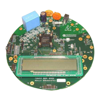
Page 90: Figure 4-10: Teridian D6513T3B2 Demo Board: Top View
71M6513/71M6513H Demo Board User’s Manual Figure 4-10: TERIDIAN D6513T3B2 Demo Board: Top View Page: 90 of 112 Revision 5.6 © 2005-2006 TERIDIAN Semiconductor Corporation Downloaded from: http://www.datasheetcatalog.com/... -
Page 91: Figure 4-11: Teridian D6513T3B2 Demo Board: Bottom View
71M6513/71M6513H Demo Board User’s Manual Figure 4-11: TERIDIAN D6513T3B2 Demo Board: Bottom View Page: 91 of 112 Revision 5.6 © 2005-2006 TERIDIAN Semiconductor Corporation Downloaded from: http://www.datasheetcatalog.com/... -
Page 92: Figure 4-12: Teridian D6513T3B2 Demo Board: Top Signal Layer
71M6513/71M6513H Demo Board User’s Manual Figure 4-12: TERIDIAN D6513T3B2 Demo Board: Top Signal Layer Page: 92 of 112 Revision 5.6 © 2005-2006 TERIDIAN Semiconductor Corporation Downloaded from: http://www.datasheetcatalog.com/... -
Page 93: Figure 4-13: Teridian D6513T3B2 Demo Board: Middle Layer 1 (Ground Plane)
71M6513/71M6513H Demo Board User’s Manual Figure 4-13: TERIDIAN D6513T3B2 Demo Board: Middle Layer 1 (Ground Plane) Page: 93 of 112 Revision 5.6 © 2005-2006 TERIDIAN Semiconductor Corporation Downloaded from: http://www.datasheetcatalog.com/... -
Page 94: Figure 4-14: Teridian D6513T3B2 Demo Board: Middle Layer 2 (Supply Plane)
71M6513/71M6513H Demo Board User’s Manual Figure 4-14: TERIDIAN D6513T3B2 Demo Board: Middle Layer 2 (Supply Plane) Page: 94 of 112 Revision 5.6 © 2005-2006 TERIDIAN Semiconductor Corporation Downloaded from: http://www.datasheetcatalog.com/... -
Page 95: Figure 4-15: Teridian D6513T3B2 Demo Board: Bottom Signal Layer
71M6513/71M6513H Demo Board User’s Manual Figure 4-15: TERIDIAN D6513T3B2 Demo Board: Bottom Signal Layer Page: 95 of 112 Revision 5.6 © 2005-2006 TERIDIAN Semiconductor Corporation Downloaded from: http://www.datasheetcatalog.com/... -
Page 96: Figure 4-16: Teridian D6513T3C1 Demo Board: Top View
71M6513/71M6513H Demo Board User’s Manual Figure 4-16: TERIDIAN D6513T3C1 Demo Board: Top View Page: 96 of 112 Revision 5.6 © 2005-2006 TERIDIAN Semiconductor Corporation Downloaded from: http://www.datasheetcatalog.com/... -
Page 97: Figure 4-17: Teridian D6513T3C1 Demo Board: Bottom View
71M6513/71M6513H Demo Board User’s Manual Figure 4-17: TERIDIAN D6513T3C1 Demo Board: Bottom View Page: 97 of 112 Revision 5.6 © 2005-2006 TERIDIAN Semiconductor Corporation Downloaded from: http://www.datasheetcatalog.com/... -
Page 98: Figure 4-18: Teridian D6513T3C1 Demo Board: Top Signal Layer
71M6513/71M6513H Demo Board User’s Manual Figure 4-18: TERIDIAN D6513T3C1 Demo Board: Top Signal Layer Page: 98 of 112 Revision 5.6 © 2005-2006 TERIDIAN Semiconductor Corporation Downloaded from: http://www.datasheetcatalog.com/... -
Page 99: Figure 4-19: Teridian D6513T3C1 Demo Board: Ground Plane Layer
71M6513/71M6513H Demo Board User’s Manual Figure 4-19: TERIDIAN D6513T3C1 Demo Board: Ground Plane Layer Page: 99 of 112 Revision 5.6 © 2005-2006 TERIDIAN Semiconductor Corporation Downloaded from: http://www.datasheetcatalog.com/... -
Page 100: Figure 4-20: Teridian D6513T3C1 Demo Board: Power Plane Layer
71M6513/71M6513H Demo Board User’s Manual Figure 4-20: TERIDIAN D6513T3C1 Demo Board: Power Plane Layer Page: 100 of 112 Revision 5.6 © 2005-2006 TERIDIAN Semiconductor Corporation Downloaded from: http://www.datasheetcatalog.com/... -
Page 101: Figure 4-21: Teridian D6513T3C1 Demo Board: Bottom Signal Layer
71M6513/71M6513H Demo Board User’s Manual Figure 4-21: TERIDIAN D6513T3C1 Demo Board: Bottom Signal Layer Page: 101 of 112 Revision 5.6 © 2005-2006 TERIDIAN Semiconductor Corporation Downloaded from: http://www.datasheetcatalog.com/... -
Page 102: Figure 4-22: Teridian D6513T3D2 Demo Board: Top Signal Layer
71M6513/71M6513H Demo Board User’s Manual Figure 4-22: TERIDIAN D6513T3D2 Demo Board: Top Signal Layer Page: 102 of 112 Revision 5.6 © 2005-2006 TERIDIAN Semiconductor Corporation Downloaded from: http://www.datasheetcatalog.com/... -
Page 103: Figure 4-23: Teridian D6513T3D2 Demo Board: Bottom Signal Layer
71M6513/71M6513H Demo Board User’s Manual Figure 4-23: TERIDIAN D6513T3D2 Demo Board: Bottom Signal Layer Page: 103 of 112 Revision 5.6 © 2005-2006 TERIDIAN Semiconductor Corporation Downloaded from: http://www.datasheetcatalog.com/... -
Page 104: Figure 4-24: Teridian D6513T3D2 Demo Board: Bottom View
71M6513/71M6513H Demo Board User’s Manual Figure 4-24: TERIDIAN D6513T3D2 Demo Board: Bottom View Page: 104 of 112 Revision 5.6 © 2005-2006 TERIDIAN Semiconductor Corporation Downloaded from: http://www.datasheetcatalog.com/... -
Page 105: Table 4-4: Debug Board: Bill Of Material
71M6513/71M6513H Demo Board User’s Manual Item Reference Value PCB Footprint Manufacturer Vendor Vendor P/N C1-C3,C5-C10,C12-C23 0.1uF 0805 C2012X7R1H104K Digi-Key 445-1349-1-ND 33uF/10V 1812 TAJB336K010R Digi-Key 478-1687-1-ND 10uF/16V, B Case 1812 TAJB106K016R Digi-Key 478-1673-1-ND D2,D3 0805 LTST-C170KGKT LITEON Digi-Key 160-1414-1-ND JP1,JP2,JP3,JP4 HDR2X1... -
Page 106: Figure 4-25: Debug Board: Electrical Schematic
71M6513/71M6513H Demo Board User’s Manual V5_DBG 0.1uF 0.1uF GND_DBG V3P3 VDD1 VDD2 V5_DBG GND2 DIO02 VDD1 DOUT GND_DBG GND1 GND2 V5_DBG V5_DBG 5Vdc EXT SUPPLY DISPLAY SEL ADUM1100 GND_DBG 0.1uF GND_DBG V5_DBG 33uF, 10V 0.1uF RAPC712 GND_DBG 0.1uF GND_DBG 0.1uF... -
Page 107: Figure 4-26: Debug Board: Top View
71M6513/71M6513H Demo Board User’s Manual Figure 4-26: Debug Board: Top View Figure 4-27: Debug Board: Bottom View Page: 107 of 112 Revision 5.6 © 2005-2006 TERIDIAN Semiconductor Corporation Downloaded from: http://www.datasheetcatalog.com/... -
Page 108: Figure 4-28: Debug Board: Top Signal Layer
71M6513/71M6513H Demo Board User’s Manual Figure 4-28: Debug Board: Top Signal Layer Figure 4-29: Debug Board: Middle Layer 1 (Ground Plane) Page: 108 of 112 Revision 5.6 © 2005-2006 TERIDIAN Semiconductor Corporation Downloaded from: http://www.datasheetcatalog.com/... -
Page 109: Figure 4-30: Debug Board: Middle Layer 2 (Supply Plane)
71M6513/71M6513H Demo Board User’s Manual Figure 4-30: Debug Board: Middle Layer 2 (Supply Plane) Figure 4-31: Debug Board: Bottom Trace Layer Page: 109 of 112 Revision 5.6 © 2005-2006 TERIDIAN Semiconductor Corporation Downloaded from: http://www.datasheetcatalog.com/... -
Page 110: Table 4-5: 71M6513/71M6513H Pin Description Table 1/3
VLCD LCD power supply. 32,33,36, 42,43,44, No Connect 47,55,90,95 Table 4-5: 71M6513/71M6513H Pin Description Table 1/3 Analog Pins: Name Type Description Line Current Sense Inputs: These pins are voltage inputs to the internal A/D converter. Typically, they are connected to the output of a current transformer. -
Page 111: Table 4-7: 71M6513/71M6513H Pin Description Table 3/3
Emulator handshake. This pin has an internal pull-up resistor. E_TCLK Emulator clock. This pin has an internal pull-up resistor. E_RST Emulator reset. This pin has an internal pull-up resistor. Table 4-7: 71M6513/71M6513H Pin Description Table 3/3 Page: 111 of 112 Revision 5.6 © 2005-2006 TERIDIAN Semiconductor Corporation Downloaded from: http://www.datasheetcatalog.com/... -
Page 112: Figure 4-32: Teridian 71M6513/71M6513H Eplqfp100: Pinout (Top View)
Figure 4-32: TERIDIAN 71M6513/71M6513H epLQFP100: Pinout (top view) User’s Manual: This User’s Manual contains proprietary product definition information of TERIDIAN Semiconductor Corporation (TSC) and is made available for informational purposes only. TERIDIAN assumes no obligation regarding future manufacture, unless agreed to in writing. - Page 113 This datasheet has been downloaded from: www.DatasheetCatalog.com Datasheets for electronic components. Downloaded from: http://www.datasheetcatalog.com/...
Need help?
Do you have a question about the 71M6513 and is the answer not in the manual?
Questions and answers