
Related Manuals for Teridian 73S8023C


Summary of Contents for Teridian 73S8023C
- Page 1 Simplifying System Integration 73S8023C Demo Board User Manual November 11, 2009 Rev. 1.3 UM_8023C_027...
- Page 2 Simplifying System Integration is a trademark of Teridian Semiconductor Corporation. All other trademarks are the property of their respective owners. Teridian Semiconductor Corporation makes no warranty for the use of its products, other than expressly contained in the Company’s warranty detailed in the Teridian Semiconductor Corporation standard Terms and Conditions.
-
Page 3: Table Of Contents
Design Considerations ........................ 12 4.1 General Layout Rules ......................12 4.2 Optimization for Compliance with EMV and NDS ..............12 73S8023C Demo Board Schematics, PCB Layouts and Bill of Materials ........13 5.1 Schematic ..........................13 5.2 Bill of Materials ........................14 5.3 PCB Layouts .......................... - Page 4 Figure 1: 73S8023C Demo Board ......................5 Figure 2: 73S8023C Demo Board Basic Connections ................6 Figure 3: 73S8023C Demo Board Connectors, Jumpers and Test Points ..........8 Figure 4: 73S8023C 32QFN Pinout (Top View) ..................11 Figure 5: 73S8023C Demo Board Electrical Schematic ................13 Figure 6: 73S8023C Demo Board Top View ...................
-
Page 5: Introduction
73S1121F evaluation platform. The board has been designed to comply with the EMV 2000 Specification, Version 4.0. 73S8023C Demo Boards can easily be modified to comply with NDS specifications by replacing a few external components that are highlighted in this document. -
Page 6: Basic Connections
CLKDIV1 = 0, CLKDIV2 =1 clock frequency = 3 MHz CLKDIV1 = 1, CLKDIV2 =0 clock frequency = 12 MHz CLKDIV1 = CLKDIV2 = 1 clock frequency = 6 MHz Figure 2: 73S8023C Demo Board Basic Connections Rev. 1.3... -
Page 7: Hardware Description
3 Hardware Description Demo Board Connectors, Jumpers and Test Points Table 1 describes the 73S8023C Demo Board connectors, jumpers and test points. The Item # in Table 1 refers to Figure 3. Table 1: 73S8023C Demo Board Connector, Jumper and Test Points... -
Page 8: Figure 3: 73S8023C Demo Board Connectors, Jumpers And Test Points
Factory test pin. Do not connect. 2-pin test points for each respective smart card signal. The pin label name is the respective signal (i.e. VCC, CLK) and the 2nd pin is GND. Figure 3: 73S8023C Demo Board Connectors, Jumpers and Test Points Rev. 1.3... -
Page 9: Recommended Operating Conditions And Absolute Maximum Ratings
ESD Tolerance – Other pins +/- 2 kV ESD testing on Card pins is HBM condition, 3 pulses, each polarity referenced to ground. 73S8023C Pin Description Table 4: 73S8023C Card Interface Pins Name Pin # Description Card I/O: Data signal to/from card. Includes a pull-up resistor to V AUX1 AUX1: Auxiliary data signal to/from card. -
Page 10: Table 5: 73S8023C Miscellaneous Pins
PWRDN Power Down control input. Active high. When the Power Down mode is set high, all internal analog functions are disabled to place the 73S8023C in its lowest power consumption mode. The Power Down mode is only allowed out of a card session (i.e. when CMDVCC = 1) Sets the divide ratio from the XTAL oscillator (or external clock input) to the card clock. -
Page 11: 73S8023C Pinout
STROBE are latched. I/OUC, AUX1UC, and AUX2UC are set to high- impedance pull-up mode (3 µA pull-up to VDD) and do not pass data to or from the smart card. 73S8023C Pinout XTALOUT XTALIN 73S8023C PRDWN PRES RSTIN CMDVCC PRES VDDF_ADJ Figure 4: 73S8023C 32QFN Pinout (Top View) Rev. 1.3... -
Page 12: Design Considerations
73S8023C Demo Board User Manual UM_8023C_027 4 Design Considerations General Layout Rules • Route the auxiliary signals away from card interface signals. • Keep the CLK signal as short as possible and with few bends in the trace. Keep the route of the CLK trace to one layer (avoid vias to other plane). -
Page 13: 73S8023C Demo Board Schematics, Pcb Layouts And Bill Of Materials
UM_8023C_027 73S8023C Demo Board User Manual 5 73S8023C Demo Board Schematics, PCB Layouts and Bill of Materials Schematic SCLK SCLK XTALIN SELECT OFFB XTAL STROBE 3.3V 5.0V JP10 SELECT SSM_110_L_SV 3.3V MUST SELECT 3.3V Resistors are CLKOUT not populated SCLK... -
Page 14: Bill Of Materials
73S8023C Demo Board User Manual UM_8023C_027 Bill of Materials Table 8 provides the bill of materials for the 73S8023C Demo Board schematic provided in Figure 5. Table 8: 73S8023C Demo Board Bill of Materials Digikey Part Item Quantity Reference Part... -
Page 15: Pcb Layouts
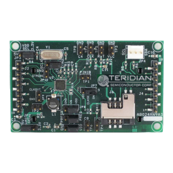
UM_8023C_027 73S8023C Demo Board User Manual PCB Layouts Figure 6: 73S8023C Demo Board Top View Figure 7: 73S8023C Demo Board Bottom View Rev. 1.3... -
Page 16: Figure 8: 73S8023C Demo Board Top Signal Layer
73S8023C Demo Board User Manual UM_8023C_027 Figure 8: 73S8023C Demo Board Top Signal Layer Figure 9: 73S8023C Demo Board Middle Layer 1, Ground Plane Rev. 1.3... -
Page 17: Figure 10: 73S8023C Middle Layer 2, Supply Plane
UM_8023C_027 73S8023C Demo Board User Manual Figure 10: 73S8023C Middle Layer 2, Supply Plane Figure 11: 73S8023C Demo Board Bottom Signal Layer Rev. 1.3... -
Page 18: Ordering Information
73S8023C Demo Board User Manual UM_8023C_027 6 Ordering Information Table 9 lists the order number used to identify the 73S8023C Demo Board. Table 9: Order Number Part Description Order Number 73S8023C 32-Pin QFN Demo Board 73S8023C-DB 7 Related Documentation The following 73S8023C documents are available from Teridian Semiconductor Corporation:... -
Page 19: Revision History
UM_8023C_027 73S8023C Demo Board User Manual Revision History Revision Date Description 8/3/2004 First publication. 11/26/2004 Minor corrections. 8/23/2005 Added new logo. 11/11/2009 Added Section 1.1, Package Contents. Added Section 1.2, Safety and ESD Notes. Added Section 6, Ordering Information. Added Section 7, Related Documentation. - Page 20 Mouser Electronics Authorized Distributor Click to View Pricing, Inventory, Delivery & Lifecycle Information: Maxim Integrated 73S8023C-DB...
Need help?
Do you have a question about the 73S8023C and is the answer not in the manual?
Questions and answers