
Related Manuals for Teridian 73S8009C


Summary of Contents for Teridian 73S8009C
- Page 1 Simplifying System Integration 73S8009C Demo Board User Manual February 10, 2010 Rev. 1.3 UM_8009C_059...
- Page 2 Simplifying System Integration is a trademark of Teridian Semiconductor Corporation. All other trademarks are the property of their respective owners. Teridian Semiconductor Corporation makes no warranty for the use of its products, other than expressly contained in the Company’s warranty detailed in the Teridian Semiconductor Corporation standard Terms and Conditions.
-
Page 3: Table Of Contents
4.3.1 USB Power ......................... 12 4.3.2 Single Supply Power ....................12 4.4 ON/OFF Switch Operation ..................... 13 73S8009C Demo Board Schematics, PCB Layouts and Bill of Materials ........14 5.1 Schematics ..........................14 5.2 73S8009C PCB Layouts ......................15 5.3 73S8009C Demo Board Bill of Materials................. 18 Errata ............................ - Page 4 Figure 6: 73S8009C Demo Board: Bottom View ..................15 Figure 7: 73S8009C Demo Board: Top Signal Layer ................16 Figure 8: 73S8009C Demo Board: Middle Layer 1, Ground Plane ............16 Figure 9: 73S8009C Demo Board: Middle Layer 2, Supply Plane ............17 Figure 10: 73S8009C Demo Board: Bottom Signal Layer ...............
-
Page 5: Introduction
The Teridian Semiconductor Corporation 73S8009C Demo Board is a platform for evaluating the Teridian 73S8009C 32-pin QFN Smart Card Interface IC. It incorporates the 73S8009C integrated circuit, and it is designed to operate either as a standalone platform (to be used in conjunction with an external microcontroller) or as a daughter card to be used in conjunction with the 73S12xxF evaluation platform. -
Page 6: Recommended Operating Conditions And Absolute Maximum Ratings
The 73S12xxF Evaluation Board has two power supplies; 3.3 V and 5.0 V. Normally, the 5.0 V supply is tied to VPC IN on the 73S8009C board. The 73S8009C can supply the 3.3 V to the remainder of the system by configuring the jumpers accordingly. The 73S8009C VDD output can be disconnected from the rest of the evaluation board if desired and the 3.3 V supply on the 73S12xxF Evaluation Board can be... -
Page 7: Connections
73S8009C Demo Board User Manual 2 Connections This section describes the 73S8009C Demo Board external connectors. All the digital signals and power supply connections are made through 10-pin header connectors labeled J2 and J4 in Figure 2. Figure 2: 73S8009C Demo Board External Connectors Table 3 describes the pins for the J4 connector. -
Page 8: Table 4: J2 Pin Descriptions
73S8009C Demo Board User Manual UM_8009C_059 Table 4 describes the J2 connector pins. Table 4: J2 Pin Descriptions Pin Name Function SCLK Clock source input. I/OUC System controller data I/O to/from the card. System controller auxiliary data C4 to/from the card. -
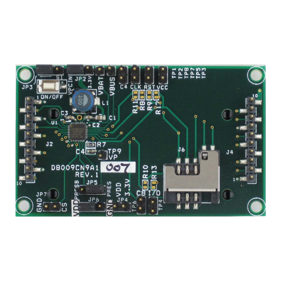
Page 9: Jumpers, Switches And Test Points
UM_8009C_059 73S8009C Demo Board User Manual 3 Jumpers, Switches and Test Points The items marked in Figure 3 are described in Table 5. Figure 3: 73S8009C Demo Board Description Rev. 1.3... -
Page 10: Table 5: 73S8009C Demo Board Description
Note: OFF_ACK must be set high to turn off. ON_OFF Jumper When set to 1-2, the ON_OFF input is set to ground which turns on the 73S8009C when power is applied. When set to 2-3, the push button switch is connected to the ON_OFF pin. - Page 11 (whether switch is nominally open or closed), and which of the card presence switch input of the 73S8009C is used. In this demo board, the switch is nominally open. The jumpers can be set in one of two ways: 1.
-
Page 12: Design Considerations
VBUS to VBAT when the VBUS power is removed. This switch over is done smoothly and does not cause any disruption of the operation of the 73S8009C and the VDD output supply. The operation of the ON/OFF switch is overridden when VBUS is applied. The 73S8009C and VDD output will always be active while the VBUS voltage is applied. -
Page 13: On/Off Switch Operation
When VBUS is removed, the latched state of the ON/OFF switch input dictates the state of the 73S8009C. If the switch input was not closed, the state of this latch will not change. It will be in the same state before the VBUS power was applied. If it has changed it holds the last toggled state. -
Page 14: 73S8009C Demo Board Schematics, Pcb Layouts And Bill Of Materials
73S8009C Demo Board User Manual UM_8009C_059 5 73S8009C Demo Board Schematics, PCB Layouts and Bill of Materials Schematics 3.3V VPCIN SCLK SELECT 3.3V 3.3V 10uF Note: JP4 pins 1 and 2 must not be 0.1uF VPCIN C1, C2, C3 and L1 must be placed... -
Page 15: 73S8009C Pcb Layouts
UM_8009C_059 73S8009C Demo Board User Manual 73S8009C PCB Layouts Figure 5: 73S8009C Demo Board: Top View Figure 6: 73S8009C Demo Board: Bottom View Rev. 1.3... -
Page 16: Figure 7: 73S8009C Demo Board: Top Signal Layer
73S8009C Demo Board User Manual UM_8009C_059 Figure 7: 73S8009C Demo Board: Top Signal Layer Figure 8: 73S8009C Demo Board: Middle Layer 1, Ground Plane Rev. 1.3... -
Page 17: Figure 9: 73S8009C Demo Board: Middle Layer 2, Supply Plane
UM_8009C_059 73S8009C Demo Board User Manual Figure 9: 73S8009C Demo Board: Middle Layer 2, Supply Plane Figure 10: 73S8009C Demo Board: Bottom Signal Layer Rev. 1.3... -
Page 18: 73S8009C Demo Board Bill Of Materials
6 Errata The 73S8009C Demo Board contains a silk screen error on JP6. The VDD and GND are reversed and have corrective decals attached to show the proper labeling. Rev. 1.3... -
Page 19: Ordering Information
UM_8009C_059 73S8009C Demo Board User Manual 7 Ordering Information Table 7 lists the order number used to identify the 73S8009C Demo Board. Table 7: 73S8009C Demo Board Order Number Part Description Order Number 73S8009C 32-Pin QFN Demo Board 73S8009C-DB 8 Related Documentation... -
Page 20: Revision History
73S8009C Demo Board User Manual UM_8009C_059 Revision History Revision Date Description 5/22/2007 First publication. 8/9/2007 Corrected schematic error. 9/6/2007 Corrected pin number for OFF_ACK in pin description. 2/10/2010 Formatted in the new Teridian style. Added Section 1.1, Package Contents. Added Section 1.2, Safety and ESD Notes. - Page 21 Mouser Electronics Authorized Distributor Click to View Pricing, Inventory, Delivery & Lifecycle Information: Maxim Integrated 73S8009C-DB...
Need help?
Do you have a question about the 73S8009C and is the answer not in the manual?
Questions and answers