Table of Contents
Advertisement
Quick Links
To our customers,
st
On April 1
, 2010, NEC Electronics Corporation merged with Renesas Technology
Corporation, and Renesas Electronics Corporation took over all the business of both
companies. Therefore, although the old company name remains in this document, it is a valid
Renesas Electronics document. We appreciate your understanding.
Issued by: Renesas Electronics Corporation (http://www.renesas.com)
Send any inquiries to http://www.renesas.com/inquiry.
Old Company Name in Catalogs and Other Documents
Renesas Electronics website: http://www.renesas.com
st
April 1
, 2010
Renesas Electronics Corporation
Advertisement
Table of Contents

Related Manuals for Renesas 78K0 Series


Summary of Contents for Renesas 78K0 Series
- Page 1 On April 1 , 2010, NEC Electronics Corporation merged with Renesas Technology Corporation, and Renesas Electronics Corporation took over all the business of both companies. Therefore, although the old company name remains in this document, it is a valid Renesas Electronics document. We appreciate your understanding.
- Page 2 Renesas Electronics. Renesas Electronics shall not be in any way liable for any damages or losses incurred by you or third parties arising from the use of any Renesas Electronics product for an application categorized as “Specific”...
- Page 3 User’s Manual 78K0/Kx2-A 8-Bit Single-Chip Microcontrollers μPD78F0590 μPD78F0591 μPD78F0592 μPD78F0593 Document No. U19780EJ2V0UD00 (2nd edition) Date Published February 2010 NS 2010 Printed in Japan...
- Page 4 [MEMO] User’s Manual U19780EJ2V0UD...
- Page 5 NOTES FOR CMOS DEVICES (1) VOLTAGE APPLICATION WAVEFORM AT INPUT PIN: Waveform distortion due to input noise or a reflected wave may cause malfunction. If the input of the CMOS device stays in the area between VIL (MAX) and VIH (MIN) due to noise, etc., the device may malfunction.
- Page 6 EEPROM is a trademark of NEC Electronics Corporation. SuperFlash is a registered trademark of Silicon Storage Technology, Inc. in several countries including the United States and Japan. ® Caution: This product uses SuperFlash technology licensed from Silicon Storage Technology, Inc. •...
- Page 7 INTRODUCTION Readers This manual is intended for user engineers who wish to understand the functions of the 78K0/Kx2-A microcontrollers and design and develop application systems and programs for these devices. Purpose This manual is intended to give users an understanding of the functions described in the Organization below.
- Page 8 Related Documents The related documents indicated in this publication may include preliminary versions. However, preliminary versions are not marked as such. Documents Related to Devices Document Name Document No. 78K0/Kx2-A User’s Manual This manual 78K/0 Series Instructions User’s Manual U12326E Documents Related to Development Tools (Software) Document Name Document No.
- Page 9 Documents Related to Development Tools (Hardware) (User’s Manual) Document Name Document No. QB-MINI2 On-Chip Debug Emulator with Programming Function U18371E Documents Related to Flash Memory Programming (User’s Manual) Document Name Document No. PG-FP5 Flash Memory Programmer U18865E QB-Programmer Programming GUI Operation U18527E Other Documents Document Name...
-
Page 10: Table Of Contents
CONTENTS CHAPTER 1 OUTLINE ..........................16 1.1 Features............................16 1.2 Applications ..........................17 1.3 Ordering Information........................17 1.4 Pin Configuration (Top View) ...................... 18 1.4.1 78K0/KB2-A ............................ 18 1.4.2 78K0/KC2-A ............................ 20 1.5 Block Diagram ..........................22 1.5.1 78K0/KB2-A ............................ 22 1.5.2 78K0/KC2-A ............................ - Page 11 3.3.1 Relative addressing .........................67 3.3.2 Immediate addressing........................68 3.3.3 Table indirect addressing.........................69 3.3.4 Register addressing .........................70 3.4 Operand Address Addressing ....................70 3.4.1 Implied addressing...........................70 3.4.2 Register addressing .........................71 3.4.3 Direct addressing ..........................72 3.4.4 Short direct addressing ........................73 3.4.5 Special function register (SFR) addressing..................74 3.4.6 Register indirect addressing ......................75 3.4.7 Based addressing ..........................76 3.4.8 Based indexed addressing.......................77...
- Page 12 5.6.1 Example of controlling high-speed system clock................148 5.6.2 Example of controlling internal high-speed oscillation clock............151 5.6.3 Example of controlling subsystem clock..................154 5.6.4 Example of controlling internal low-speed oscillation clock ............156 5.6.5 Clocks supplied to CPU and peripheral hardware................157 5.6.6 CPU clock status transition diagram ....................158 5.6.7 Condition before changing CPU clock and processing after changing CPU clock ......164 5.6.8 Time required for switchover of CPU clock and main system clock ..........166 5.6.9 Conditions before clock oscillation is stopped ................168...
- Page 13 8.4.3 Carrier generator operation (8-bit timer H1 only) ................278 CHAPTER 9 REAL-TIME COUNTER ....................285 9.1 Functions of Real-Time Counter....................285 9.2 Configuration of Real-Time Counter ..................286 9.3 Registers Controlling Real-Time Counter ................288 9.4 Real-Time Counter Operation ....................301 9.4.1 Starting operation of real-time counter...................301 9.4.2 Reading/writing real-time counter ....................302 9.4.3 Setting alarm of real-time counter ....................304...
- Page 14 13.4 Operation of Operational Amplifier ..................361 CHAPTER 14 SERIAL INTERFACE UART6 ..................362 14.1 Functions of Serial Interface UART6 ..................362 14.2 Configuration of Serial Interface UART6 ................367 14.3 Registers Controlling Serial Interface UART6............... 370 14.4 Operation of Serial Interface UART6 ..................379 14.4.1 Operation stop mode........................379 14.4.2 Asynchronous serial interface (UART) mode ................380 14.4.3 Dedicated baud rate generator.....................394...
- Page 15 CHAPTER 17 MULTIPLIER/DIVIDER....................501 17.1 Functions of Multiplier/Divider ....................501 17.2 Configuration of Multiplier/Divider..................501 17.3 Register Controlling Multiplier/Divider .................. 505 17.4 Operations of Multiplier/Divider....................506 17.4.1 Multiplication operation ........................506 17.4.2 Division operation ........................508 CHAPTER 18 INTERRUPT FUNCTIONS .................... 510 18.1 Interrupt Function Types......................
- Page 16 23.4.1 When used as reset ........................573 23.4.2 When used as interrupt ........................578 23.5 Cautions for Low-Voltage Detector ..................583 CHAPTER 24 OPTION BYTE....................... 586 24.1 Functions of Option Bytes ...................... 586 24.2 Format of Option Byte ......................587 CHAPTER 25 FLASH MEMORY ......................591 25.1 Internal Memory Size Switching Register................
- Page 17 29.2 78K0/KC2-A..........................655 CHAPTER 30 CAUTIONS FOR WAIT ....................656 30.1 Cautions for Wait ........................656 30.2 Peripheral Hardware That Generates Wait ................656 User’s Manual U19780EJ2V0UD...
-
Page 18: Chapter 1 Outline
CHAPTER 1 OUTLINE 1.1 Features μ Minimum instruction execution time can be changed from high speed (0.1 s: @ 20 MHz operation with high- μ Note1 speed system clock) to ultra low-speed (122 s: @ 32.768 kHz operation with subsystem clock General-purpose register: 8 bits ×... -
Page 19: Applications
CHAPTER 1 OUTLINE Serial interface Item UART supporting LIN-bus 3-wire CSI Part Number 78K0/KB2-A 1 channel 1 channel 1 channel Note 78K0/KC2-A 1 channel Note Enable control is possible when the 3-wire CSI is used as a slave. Power supply voltage: V = 1.8 to 5.5 V Operating ambient temperature: T = –40 to +85°C... -
Page 20: Pin Configuration (Top View)
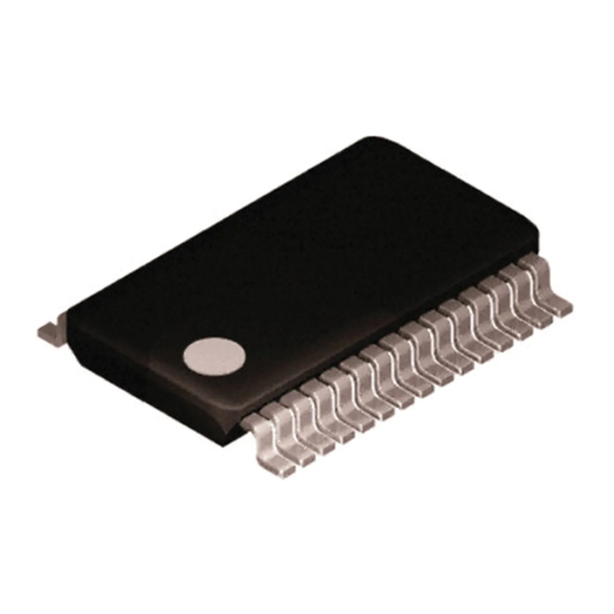
CHAPTER 1 OUTLINE 1.4 Pin Configuration (Top View) 1.4.1 78K0/KB2-A • 30-pin plastic SSOP (7.62 mm (300)) P23/ANI3/AMP1- P24/ANI4/AMP1OUT P22/ANI2/AMP0+ P25/ANI5/AMP1+ P21/ANI1/AMP0OUT P20/ANI0/AMP0- P120/INTP0/EXLVI RESET P80/ANI8/AMP2- FLMD0 P81/ANI9/AMP2OUT P122/X2/EXCLK/OCD0B P82/ANI10/AMP2+ P83/ANI11 P121/X1/OCD0A REGC P10/TxD6/TI51/TO51 P11/RxD6/TI50/TO50 P12/TOH0/INTP7/TI000 P60/SCLA0/SCK10 P13/TOH1/INTP6/TI010/TO00 P61/SDAA0/SI10 P31/INTP5/OCD1A (/SCK10) P35/SO10/INTP1 P32/INTP4/OCD1B (/SI10) Cautions 1. - Page 21 CHAPTER 1 OUTLINE Pin Identification AMP0− to AMP2−: Amplifier Input Minus P80 to P83: Port 8 AMP0+ to AMP2+: Amplifier Input Plus P120 to P122: Port 12 AMP0OUT REGC: Regulator Capacitance to AMP2OUT: Amplifier Output RESET: Reset ANI0 to ANI5, RxD6: Receive Data ANI8 to ANI11:...
-
Page 22: 78K0/Kc2-A
CHAPTER 1 OUTLINE 1.4.2 78K0/KC2-A • 48-pin plastic LQFP (fine pitch) (7x7) 48 47 46 45 44 43 42 41 40 39 38 37 P60/SCLA0/SCK10 P42/PCL/SSI10/INTP9 P61/SDAA0/SI10 P00/TI000 P35/SO10/INTP1 P01/TI010/TO00 P34/TI50/TO50/INTP2 P02/INTP8 P33/TI51/TO51/INTP3 P20/ANI0/AMP0- P75/KR5 P21/ANI1/AMP0OUT P74/KR4 P22/ANI2/AMP0+ P73/KR3 P23/ANI3/AMP1- P72/KR2 P24/ANI4/AMP1OUT P71/KR1... - Page 23 CHAPTER 1 OUTLINE Pin Identification AMP0− to AMP2−: Amplifier Input Minus PCL: Programmable Clock Output AMP0+ to AMP2+: Amplifier Input Plus REGC: Regulator Capacitance AMP0OUT RESET: Reset to AMP2OUT: Amplifier Output RTC1HZ: Real-time Counter Correction ANI0 to ANI6, Clock (1 Hz) Output ANI8 to ANI11, RTCCL: Real-time Counter Clock...
-
Page 24: Block Diagram
CHAPTER 1 OUTLINE 1.5 Block Diagram 1.5.1 78K0/KB2-A TO00/TI010/P13 16-bit TIMER/ PORT 1 P10 to P13 EVENT COUNTER 00 TI000/P12 RxD6/P11[LINSEL] PORT 2 P20 to P25 TOH0/P12 8-bit TIMER H0 PORT 3 P31, P32, P35 TOH1/P13 8-bit TIMER H1 PORT 6 P60, P61 INTERNAL PORT 8... -
Page 25: 78K0/Kc2-A
CHAPTER 1 OUTLINE 1.5.2 78K0/KC2-A TO00/TI010/P01 16-bit TIMER/ PORT 0 P00 to P02 EVENT COUNTER 00 TI000/P00 RxD6/P11 [LINSEL] PORT 1 P10 to P13 TOH0/P12 8-bit TIMER H0 PORT 2 P20 to P27 TOH1/P13 8-bit TIMER H1 PORT 3 P31 to P35 PORT 4 P40 to P42 INTERNAL... -
Page 26: Outline Of Functions
CHAPTER 1 OUTLINE 1.6 Outline of Functions Part Number 78K0/KB2-A 78K0/KC2-A μ μ μ μ PD78F0590 PD78F0591 PD78F0592 PD78F0593 Item 30 Pins 48 Pins Flash memory (Self- 16 KB 32 KB 16 KB 32 KB Internal programming supported) memory High-speed RAM 1 KB Power supply voltage = 1.8 to 5.5 V... -
Page 27: Chapter 2 Pin Functions
CHAPTER 2 PIN FUNCTIONS 2.1 Pin Function List There are two types of pin I/O buffer power supplies: AV and V . The relationship between these power supplies and the pins is shown below. Table 2-1. Pin I/O Buffer Power Supplies Power Supply Corresponding Pins 78K0/KB2-A... -
Page 28: 78K0/Kb2-A
CHAPTER 2 PIN FUNCTIONS 2.1.1 78K0/KB2-A (1) Port functions: 78K0/KB2-A Function Name Function After Reset Alternate Function Port 1. Input port TxD6/TI51/TO51 4-bit I/O port. RxD6/TI50/TO50 Input/output can be specified in 1-bit units. TOH0/INTP7/TI000 Use of an on-chip pull-up resistor can be specified by a software TOH1/INTP6/TI010 setting. - Page 29 CHAPTER 2 PIN FUNCTIONS (2) Non-port functions (1/2): 78K0/KB2-A Function Name Function After Reset Alternate Function AMP0− Input Operational amplifier (−) input Digital input ANI0/P20 port AMP1− ANI3/P23 AMP2− ANI8/P80 AMP0+ Input Operational amplifier (+) input Digital input ANI2/P22 port AMP1+ ANI5/P25 AMP2+...
- Page 30 CHAPTER 2 PIN FUNCTIONS (2) Non-port functions (2/2): 78K0/KB2-A Function Name Function After Reset Alternate Function SI10 Input Serial data input to CSI10 Input port P61/SDAA0 (SI10) P32/OCD1B SO10 P35/INTP1 Output Serial data output from CSI10 Input port TI000 P12/TOH0/INTP7 Input External count clock input to 16-bit timer/event counter 00 Input port...
-
Page 31: 78K0/Kc2-A
CHAPTER 2 PIN FUNCTIONS 2.1.2 78K0/KC2-A (1) Port functions (1/2): 78K0/KC2-A Function Name Function After Reset Alternate Function Port 0. Input port TI000 3-bit I/O port. TI010/TO00 Input/output can be specified in 1-bit units. INTP8 Use of an on-chip pull-up resistor can be specified by a software setting. - Page 32 CHAPTER 2 PIN FUNCTIONS (1) Port functions (2/2): 78K0/KC2-A Function Name Function After Reset Alternate Function Port 8. Digital ANI8/AMP2− 4-bit I/O port. input port ANI9/AMP2OUT Input/output can be specified in 1-bit units. ANI10/AMP2+ ANI11 P120 Port 12. Input port INTP0/EXLVI 5-bit I/O port.
- Page 33 CHAPTER 2 PIN FUNCTIONS (2) Non-port functions (1/3): 78K0/KC2-A Function Name Function After Reset Alternate Function AMP0− Input Operational amplifier (−) input Digital ANI0/P20 input port AMP1− ANI3/P23 AMP2− ANI8/P80 AMP0+ Input Operational amplifier (+) input Digital ANI2/P22 input port AMP1+ ANI5/P25 AMP2+...
- Page 34 CHAPTER 2 PIN FUNCTIONS (2) Non-port functions (2/3): 78K0/KC2-A Function Name Function After Reset Alternate Function − − − REGC Connecting regulator output (2.5 V) stabilization capacitance for internal operation. μ Connect to V via a capacitor (0.47 to 1 F: recommended).
- Page 35 CHAPTER 2 PIN FUNCTIONS (2) Non-port functions (3/3): 78K0/KC2-A Function Name Function After Reset Alternate Function − − − Positive power supply for pins other than P20 to P27, P80 to P83, A/D converter, and operational amplifier. − − − Positive power supply for pins P20 to P27, P80 to P83, A/D converter, and operational amplifier.
-
Page 36: Description Of Pin Functions
CHAPTER 2 PIN FUNCTIONS 2.2 Description of Pin Functions Remark The pins mounted depend on the product. See 1.4 Ordering Information and 2.1 Pin Function List. 2.2.1 P00 to P02 (port 0) P00 to P02 function as an I/O port. These pins also function as external interrupt request input and timer I/O. 78K0/KB2-A 78K0/KC2-A −... -
Page 37: P10 To P13 (Port 1)
CHAPTER 2 PIN FUNCTIONS 2.2.2 P10 to P13 (port 1) P10 to P13 function as an I/O port. These pins also function as pins for external interrupt request input, serial interface data I/O, and timer I/O. 78K0/KB2-A 78K0/KC2-A P10/TxD6/TI51/TO51 P10/TxD6 P11/RxD6/TI50/TO50 P11/RxD6 P12/TOH0/INTP7/TI000... -
Page 38: P20 To P27 (Port 2)
CHAPTER 2 PIN FUNCTIONS (h) TI010 This is the pin for inputting a capture trigger signal to the capture register (CR000) of 16-bit timer/event counter 00. TO00 This is the timer output pin of 16-bit timer/event counter 00. 2.2.3 P20 to P27 (port 2) P20 to P27 function as an I/O port. -
Page 39: P31 To P35 (Port 3)
CHAPTER 2 PIN FUNCTIONS 2.2.4 P31 to P35 (port 3) P31 to P35 function as an I/O port. These pins also function as pins for external interrupt request input, serial interface data I/O, clock I/O, and timer I/O. 78K0/KB2-A 78K0/KC2-A P31/INTP5/OCD1A (/SCK10) P32/INTP4/OCD1B (/SI10) −... -
Page 40: P40 To P42 (Port 4)
CHAPTER 2 PIN FUNCTIONS Caution Process the P31/INTP5/OCD1A (/SCK10) pin as follows, when it is not used when it is connected to a flash memory programmer or an on-chip debug emulator. P31/INTP5/OCD1A (/SCK10) Flash memory programmer connection Connect to V via a resistor. -
Page 41: P60, P61 (Port 6)
CHAPTER 2 PIN FUNCTIONS (e) RTC1HZ This is a real-time counter correction clock (1 Hz) output pin. (f) SSI10 This is a chip select input pin for serial interface CSI10. 2.2.6 P60, P61 (Port 6) P60 and P61 function as an I/O port. These pins also function as pins for serial interface data I/O and clock I/O. 78K0/KB2-A 78K0/KC2-A P60/SCLA0/SCK10... -
Page 42: P70 To P75 (Port 7)
CHAPTER 2 PIN FUNCTIONS 2.2.7 P70 to P75 (port 7) P70 to P75 function as an I/O port. These pins also function as key interrupt input pins. 78K0/KB2-A 78K0/KC2-A − P70/KR0 P71/KR1 P72/KR2 P73/KR3 P74/KR4 P75/KR5 The following operation modes can be specified in 1-bit units. (1) Port mode P70 to P75 function as an I/O port. -
Page 43: P120 To P124 (Port 12)
CHAPTER 2 PIN FUNCTIONS (a) ANI8 to ANI11 P80 to P83 function as A/D converter analog input pins. When using these pins as analog input pins, see (5) ANI0 to ANI6, ANI8 to ANI11, and ANI15 in 12.6 Cautions for A/D Converter. (b) AMP2−... -
Page 44: Av , Av , Av , Av , Av
CHAPTER 2 PIN FUNCTIONS (c) X1, X2 These are the pins for connecting a resonator for main system clock. (d) EXCLK This is an external clock input pin for main system clock. (e) XT1, XT2 These are the pins for connecting a resonator for subsystem clock. Caution Process the P121/X1/OCD0A pin as follows, when it is not used when it is connected to a flash memory programmer or an on-chip debug emulator. -
Page 45: Reset
CHAPTER 2 PIN FUNCTIONS (d) AV is the positive power supply pin for P20 to P27, P80 to P83, A/D converter, and operational amplifier. Note Even when the A/D converter or operational amplifier is not used, connect this pin directly to V Note Make the AV pin the same potential as the V pin when port 2 and port 8 are used as a digital port. -
Page 46: Pin I/O Circuits And Recommended Connection Of Unused Pins
CHAPTER 2 PIN FUNCTIONS 2.3 Pin I/O Circuits and Recommended Connection of Unused Pins Table 2-2 shows the types of pin I/O circuits and the recommended connections of unused pins. See Figure 2-1 for the configuration of the I/O circuit of each type. Remark The pins mounted depend on the product. - Page 47 CHAPTER 2 PIN FUNCTIONS Table 2-2. Pin I/O Circuit Types (2/3) Pin Name I/O Circuit Type Recommended Connection of Unused Pins P31/INTP5/OCD1A 5-AQ Input: Independently connect to V or V via a resistor. Output: Leave open. Note 1 (/SCK10) P32/INTP4/OCD1B (/SI10) P33/TI51/TO51/INTP3 P34/TI50/TO50/INTP2 P35/SO10/INTP1...
- Page 48 CHAPTER 2 PIN FUNCTIONS Table 2-2. Pin I/O Circuit Types (3/3) Pin Name I/O Circuit Type Recommended Connection of Unused Pins − − <When any of P20 to P27 and P80 to P83 is specified as a digital port > Make the same potential as the V <When all of P20 to P27 and P80 to P83 are specified as analog ports >...
- Page 49 CHAPTER 2 PIN FUNCTIONS Figure 2-1. Pin I/O Circuit List (1/2) Type 2 Type 5-AG pullup P-ch enable data P-ch IN/OUT output Schmitt-triggered input with hysteresis characteristics N-ch disable input enable Type 5-AQ Type 5-AQ data P-ch pullup P-ch enable IN/OUT output N-ch...
- Page 50 CHAPTER 2 PIN FUNCTIONS Figure 2-1. Pin I/O Circuit List (2/2) Type 11-S Type 11-T data P-ch data P-ch IN/OUT IN/OUT output N-ch disable output N-ch disable P-ch Comparator P-ch Comparator N-ch N-ch (threshold voltage) (threshold voltage) input enable P-ch input enable REFM N-ch...
-
Page 51: Chapter 3 Cpu Architecture
CHAPTER 3 CPU ARCHITECTURE 3.1 Memory Space 78K0/Kx2-A microcontrollers can access a 64 KB memory space. Figures 3-1 and 3-2 show the memory maps. Caution Regardless of the internal memory capacity, the initial values of the internal memory size switching register (IMS) of 78K0/Kx2-A microcontrollers are fixed (IMS = CFH). Therefore, set the value corresponding to each product as indicated below. - Page 52 CHAPTER 3 CPU ARCHITECTURE μ Figure 3-1. Memory Map ( PD78F0590 and 78F0592) FFFFH Special function registers 3FFFH (SFR) 256 × 8 bits Program area FF00H 1FFFH FEFFH 108FH General-purpose 108EH registers On-chip debug security 32 × 8 bits Note 1 FEE0H ID setting area 10 ×...
- Page 53 CHAPTER 3 CPU ARCHITECTURE μ Figure 3-2. Memory Map ( PD78F0591 and 78F0593) FFFFH Special function registers 7FFFH (SFR) 256 × 8 bits Program area FF00H 1FFFH FEFFH 108FH General-purpose 108EH registers On-chip debug security 32 × 8 bits Note 1 FEE0H ID setting area 10 ×...
-
Page 54: Internal Program Memory Space
CHAPTER 3 CPU ARCHITECTURE Correspondence between the address values and block numbers in the flash memory are shown below. Table 3-2. Correspondence Between Address Values and Block Numbers in Flash Memory Address Value Block Number Address Value Block Number 0000H to 03FFH 4000H to 43FFH 0400H to 07FFH 4400H to 47FFH... - Page 55 CHAPTER 3 CPU ARCHITECTURE (1) Vector table area The 64-byte area 0000H to 003FH is reserved as a vector table area. The program start addresses for branch upon reset or generation of each interrupt request are stored in the vector table area. Of the 16-bit address, the lower 8 bits are stored at even addresses and the higher 8 bits are stored at odd addresses.
-
Page 56: Internal Data Memory Space
CHAPTER 3 CPU ARCHITECTURE (3) Option byte area A 5-byte area of 0080H to 0084H and 1080H to 1084H can be used as an option byte area. Set the option byte at 0080H to 0084H when the boot swap is not used, and at 0080H to 0084H and 1080H to 1084H when the boot swap is used. - Page 57 CHAPTER 3 CPU ARCHITECTURE μ Figure 3-3. Correspondence Between Data Memory and Addressing ( PD78F0590 and 78F0592) F F F F H Special function registers SFR addressing (SFR) 256 x 8 bits F F 2 0 H F F 1 F H F F 0 0 H F E F F H General-purpose...
- Page 58 CHAPTER 3 CPU ARCHITECTURE μ Figure 3-4. Correspondence Between Data Memory and Addressing ( PD78F0591 and 78F0593) F F F F H Special function registers SFR addressing (SFR) 256 x 8 bits F F 2 0 H F F 1 F H F F 0 0 H F E F F H General-purpose...
-
Page 59: Processor Registers
CHAPTER 3 CPU ARCHITECTURE 3.2 Processor Registers 78K0/Kx2-A microcontrollers incorporate the following processor registers. 3.2.1 Control registers The control registers control the program sequence, statuses and stack memory. The control registers consist of a program counter (PC), a program status word (PSW) and a stack pointer (SP). (1) Program counter (PC) The program counter is a 16-bit register that holds the address information of the next program to be executed. - Page 60 CHAPTER 3 CPU ARCHITECTURE (c) Register bank select flags (RBS0 and RBS1) These are 2-bit flags to select one of the four register banks. In these flags, the 2-bit information that indicates the register bank selected by SEL RBn instruction execution is stored.
- Page 61 CHAPTER 3 CPU ARCHITECTURE Figure 3-8. Data to Be Saved to Stack Memory (a) PUSH rp instruction (when SP = FEE0H) FEE0H FEE0H FEDFH Register pair higher FEDEH Register pair lower FEDEH (b) CALL, CALLF, CALLT instructions (when SP = FEE0H) FEE0H FEE0H FEDFH...
-
Page 62: General-Purpose Registers
CHAPTER 3 CPU ARCHITECTURE Figure 3-9. Data to Be Restored from Stack Memory (a) POP rp instruction (when SP = FEDEH) FEE0H FEE0H FEDFH Register pair higher FEDEH Register pair lower FEDEH (b) RET instruction (when SP = FEDEH) FEE0H FEE0H FEDFH PC15 to PC8... - Page 63 CHAPTER 3 CPU ARCHITECTURE Figure 3-10. Configuration of General-Purpose Registers (a) Function name 16-bit processing 8-bit processing FEFFH Register bank 0 FEF8H Register bank 1 FEF0H Register bank 2 FEE8H Register bank 3 FEE0H (b) Absolute name 16-bit processing 8-bit processing FEFFH Register bank 0 FEF8H...
-
Page 64: Special Function Registers (Sfrs)
CHAPTER 3 CPU ARCHITECTURE 3.2.3 Special function registers (SFRs) Unlike a general-purpose register, each special function register has a special function. SFRs are allocated to the FF00H to FFFFH area. Special function registers can be manipulated like general-purpose registers, using operation, transfer, and bit manipulation instructions. - Page 65 CHAPTER 3 CPU ARCHITECTURE Table 3-6. Special Function Register List (1/4) 30-pin 48-pin Address Special Function Register (SFR) Name Symbol Manipulatable Bit Unit After products products Reset 1 Bit 8 Bits 16 Bits − √ √ − √ FF00H Port register 0 √...
- Page 66 CHAPTER 3 CPU ARCHITECTURE Table 3-6. Special Function Register List (2/4) 30-pin 48-pin Address Special Function Register (SFR) Name Symbol Manipulatable Bit Unit After products products Reset 1 Bit 8 Bits 16 Bits − − √ √ √ FF30H Pull-up resistor option register 0 √...
- Page 67 CHAPTER 3 CPU ARCHITECTURE Table 3-6. Special Function Register List (3/4) 30-pin 48-pin Address Special Function Register (SFR) Name Symbol Manipulatable Bit Unit After products products Reset 1 Bit 8 Bits 16 Bits − √ √ √ √ Multiplier/divider control register 0 FF68H DMUC0 √...
- Page 68 CHAPTER 3 CPU ARCHITECTURE Table 3-6. Special Function Register List (4/4) 30-pin 48-pin Address Special Function Register (SFR) Name Symbol Manipulatable Bit Unit After products products Reset 1 Bit 8 Bits 16 Bits − √ − √ √ IICA shift register FFA6H IICA −...
-
Page 69: Instruction Address Addressing
CHAPTER 3 CPU ARCHITECTURE 3.3 Instruction Address Addressing An instruction address is determined by contents of the program counter (PC), and is normally incremented (+1 for each byte) automatically according to the number of bytes of an instruction to be fetched each time another instruction is executed. -
Page 70: Immediate Addressing
CHAPTER 3 CPU ARCHITECTURE 3.3.2 Immediate addressing [Function] Immediate data in the instruction word is transferred to the program counter (PC) and branched. This function is carried out when the CALL !addr16 or BR !addr16 or CALLF !addr11 instruction is executed. CALL !addr16 and BR !addr16 instructions can be branched to the entire memory space. - Page 71 CHAPTER 3 CPU ARCHITECTURE 3.3.3 Table indirect addressing [Function] Table contents (branch destination address) of the particular location to be addressed by bits 1 to 5 of the immediate data of an operation code are transferred to the program counter (PC) and branched. This function is carried out when the CALLT [addr5] instruction is executed.
-
Page 72: Register Addressing
CHAPTER 3 CPU ARCHITECTURE 3.3.4 Register addressing [Function] Register pair (AX) contents to be specified with an instruction word are transferred to the program counter (PC) and branched. This function is carried out when the BR AX instruction is executed. [Illustration] 3.4 Operand Address Addressing The following methods are available to specify the register and memory (addressing) to undergo manipulation... -
Page 73: Register Addressing
CHAPTER 3 CPU ARCHITECTURE 3.4.2 Register addressing [Function] The general-purpose register to be specified is accessed as an operand with the register bank select flags (RBS0 to RBS1) and the register specify codes of an operation code. Register addressing is carried out when an instruction with the following operand format is executed. When an 8-bit register is specified, one of the eight registers is specified with 3 bits in the operation code. -
Page 74: Direct Addressing
CHAPTER 3 CPU ARCHITECTURE 3.4.3 Direct addressing [Function] The memory to be manipulated is directly addressed with immediate data in an instruction word becoming an operand address. This addressing can be carried out for all of the memory spaces. [Operand format] Identifier Description addr16... -
Page 75: Short Direct Addressing
CHAPTER 3 CPU ARCHITECTURE 3.4.4 Short direct addressing [Function] The memory to be manipulated in the fixed space is directly addressed with 8-bit data in an instruction word. This addressing is applied to the 256-byte space FE20H to FF1FH. Internal high-speed RAM and special function registers (SFRs) are mapped at FE20H to FEFFH and FF00H to FF1FH, respectively. -
Page 76: Special Function Register (Sfr) Addressing
CHAPTER 3 CPU ARCHITECTURE 3.4.5 Special function register (SFR) addressing [Function] A memory-mapped special function register (SFR) is addressed with 8-bit immediate data in an instruction word. This addressing is applied to the 240-byte spaces FF00H to FFCFH and FFE0H to FFFFH. However, the SFRs mapped at FF00H to FF1FH can be accessed with short direct addressing. -
Page 77: Register Indirect Addressing
CHAPTER 3 CPU ARCHITECTURE 3.4.6 Register indirect addressing [Function] Register pair contents specified by a register pair specify code in an instruction word and by a register bank select flag (RBS0 and RBS1) serve as an operand address for addressing the memory. This addressing can be carried out for all of the memory spaces. -
Page 78: Based Addressing
CHAPTER 3 CPU ARCHITECTURE 3.4.7 Based addressing [Function] 8-bit immediate data is added as offset data to the contents of the base register, that is, the HL register pair in the register bank specified by the register bank select flag (RBS0 and RBS1), and the sum is used to address the memory. -
Page 79: Based Indexed Addressing
CHAPTER 3 CPU ARCHITECTURE 3.4.8 Based indexed addressing [Function] The B or C register contents specified in an instruction word are added to the contents of the base register, that is, the HL register pair in the register bank specified by the register bank select flag (RBS0 and RBS1), and the sum is used to address the memory. -
Page 80: Stack Addressing
CHAPTER 3 CPU ARCHITECTURE 3.4.9 Stack addressing [Function] The stack area is indirectly addressed with the stack pointer (SP) contents. This addressing method is automatically employed when the PUSH, POP, subroutine call and return instructions are executed or the register is saved/reset upon generation of an interrupt request. With stack addressing, only the internal high-speed RAM area can be accessed. -
Page 81: Chapter 4 Port Functions
CHAPTER 4 PORT FUNCTIONS 4.1 Port Functions There are two types of pin I/O buffer power supplies: AV and V . The relationship between these power supplies and the pins is shown below. Table 4-1. Pin I/O Buffer Power Supplies Power Supply Corresponding Pins 78K0/KB2-A... - Page 82 CHAPTER 4 PORT FUNCTIONS Table 4-2. Port Functions (78K0/KB2-A) Function Name Function After Reset Alternate Function Port 1. Input port TxD6/TI51/TO51 4-bit I/O port. RxD6/TI50/TO50 Input/output can be specified in 1-bit units. TOH0/INTP7/TI000 Use of an on-chip pull-up resistor can be specified by a TOH1/INTP6/TI010 software setting.
- Page 83 CHAPTER 4 PORT FUNCTIONS Table 4-3. Port Functions (78K0/KC2-A) Function Name Function After Reset Alternate Function Port 0. Input port TI000 3-bit I/O port. TI010/TO00 Input/output can be specified in 1-bit units. Use of an on-chip pull-up resistor can be specified by a INTP8 software setting.
-
Page 84: Port Configuration
CHAPTER 4 PORT FUNCTIONS 4.2 Port Configuration Ports include the following hardware. Table 4-4. Port Configuration Item Configuration • 78K0/KB2-A Control registers Port mode register (PMxx): PM1 to PM3, PM6, PM8, PM12 Port register (Pxx): P1 to P3, P6, P8, P12 Pull-up resistor option register (PUxx): PU1, PU3, PU12 A/D port configuration register (ADPC) •... -
Page 85: Port 0
CHAPTER 4 PORT FUNCTIONS 4.2.1 Port 0 78K0/KB2-A 78K0/KC2-A − P00/TI000 P01/TI010/TO00 P02/INTP8 Port 0 is an I/O port with an output latch. Port 0 can be set to the input mode or output mode in 1-bit units using port mode register 0 (PM0). When the P00 to P02 pins are used as an input port, use of an on-chip pull-up resistor can be specified in 1-bit units by pull-up resistor option register 0 (PU0). - Page 86 CHAPTER 4 PORT FUNCTIONS Figure 4-2. Block Diagram of P01 PU01 P-ch Alternate function PORT Output latch P01/TI010/TO00 (P01) PM01 Alternate function Port register 0 PU0: Pull-up resistor option register 0 PM0: Port mode register 0 Read signal WR××: Write signal User’s Manual U19780EJ2V0UD...
-
Page 87: Port 1
CHAPTER 4 PORT FUNCTIONS 4.2.2 Port 1 78K0/KB2-A 78K0/KC2-A P10/TxD6/TI51/TO51 P10/TxD6 P11/RxD6/TI50/TO50 P11/RxD6 P12/TOH0/INTP7/TI000 P12/TOH0/INTP7 P13/TOH1/INTP6/TI010/TO00 P13/TOH1/INTP6 Port 1 is an I/O port with an output latch. Port 1 can be set to the input mode or output mode in 1-bit units using port mode register 1 (PM1). - Page 88 CHAPTER 4 PORT FUNCTIONS Figure 4-3. Block Diagram of P10 (1/2) (1) 78K0/KB2-A PU10 P-ch Alternate function PORT Output latch (P10) P10/TxD6/TI51/TO51 PM10 Alternate function (Serial interface) Alternate function (Timer) Port register 1 PU1: Pull-up resistor option register 1 PM1: Port mode register 1 Read signal WR××: Write signal...
- Page 89 CHAPTER 4 PORT FUNCTIONS Figure 4-3. Block Diagram of P10 (2/2) (2) 78K0/KC2-A PU10 P-ch Alternate function PORT Output latch P10/TxD6 (P10) PM10 Alternate function Port register 1 PU1: Pull-up resistor option register 1 PM1: Port mode register 1 Read signal WR××: Write signal User’s Manual U19780EJ2V0UD...
- Page 90 CHAPTER 4 PORT FUNCTIONS Figure 4-4. Block Diagram of P11 (1/2) (1) 78K0/KB2-A PU11 P-ch Alternate function PORT Output latch P11/RxD6/TI50/TO50 (P11) PM11 Alternate function Port register 1 PU1: Pull-up resistor option register 1 PM1: Port mode register 1 Read signal WR××: Write signal User’s Manual U19780EJ2V0UD...
- Page 91 CHAPTER 4 PORT FUNCTIONS Figure 4-4. Block Diagram of P11 (2/2) (2) 78K0/KC2-A PU11 P-ch Alternate function PORT Output latch P11/RxD6 (P11) PM11 Port register 1 PU1: Pull-up resistor option register 1 PM1: Port mode register 1 Read signal WR××: Write signal User’s Manual U19780EJ2V0UD...
- Page 92 CHAPTER 4 PORT FUNCTIONS Figure 4-5. Block Diagram of P12 and P13 PU12, PU13 P-ch Alternate function PORT Output latch Note (P12, P13) P12/TOH0/INTP7/TI000 Note P13/TOH1/INTP6/TI010/TO00 PM12, PM13 Alternate function Port register 1 PU1: Pull-up resistor option register 1 PM1: Port mode register 1 Read signal WR××: Write signal...
-
Page 93: Port 2
CHAPTER 4 PORT FUNCTIONS 4.2.3 Port 2 78K0/KB2-A 78K0/KC2-A P20/ANI0/AMP0− P21/ANI1/AMP0OUT P22/ANI2/AMP0+ P23/ANI3/AMP1− P24/ANI4/AMP1OUT P25/ANI5/AMP1+ − P26/ANI6 P27/ANI15/AV REFM Port 2 is an I/O port with an output latch. Port 2 can be set to the input mode or output mode in 1-bit units using port mode register 2 (PM2). - Page 94 CHAPTER 4 PORT FUNCTIONS P20/ANI0/AMP0− to P27/ANI15/AV pins are as shown below depending on the settings of ADPC, ADS, PM2, REFM OAENn, and ADREF. Table 4-5. Setting Functions of P20/ANI0/AMP0−, P22/ANI2/AMP0+, P23/ANI3/AMP1−, P25/ANI5/AMP1+ Pins ADPC OAENn P20/ANI0/AMP0−, P22/ANI2/AMP0+, P23/ANI3/AMP1−, P25/ANI5/AMP1+ Pin −...
- Page 95 CHAPTER 4 PORT FUNCTIONS Table 4-8. Setting Functions of P27/ANI15/AV REFM ADPC ADREF P27/ANI15/AV REFM − Digital I/O Input mode Digital input selection − Setting prohibited − Output mode Digital output − Setting prohibited Analog input Input mode Selects ANI. Analog input (to be converted) selection Does not select ANI.
- Page 96 CHAPTER 4 PORT FUNCTIONS Figure 4-6. Block Diagram of P20 and P23 PORT Output latch P20/ANI0/AMP0-, (P20, P23) P23/ANI3/AMP1- PM20, PM23 A/D converter Operational amplifier (-) input Figure 4-7. Block Diagram of P21, P24 PORT Output latch P21/ANI1/AMP0OUT, (P21, P24) P24/ANI4/AMP1OUT PM21, PM24 Operational amplifier output...
- Page 97 CHAPTER 4 PORT FUNCTIONS Figure 4-8. Block Diagram of P21, P24 PORT Output latch P22/ANI2/AMP0+, (P22, P25) P25/ANI5/AMP1+ PM22, PM25 A/D converter Operational amplifier (+) input Figure 4-9. Block Diagram of P26 PORT Output latch P26/ANI6 (P26) PM26 A/D converter Port register 2 PM2: Port mode register 2...
- Page 98 CHAPTER 4 PORT FUNCTIONS Figure 4-10. Block Diagram of P27 PORT Output latch P27/ANI15/AV REFM (P27) PM27 A/D converter Analog reference voltage (-) input Port register 2 PM2: Port mode register 2 Read signal WR××: Write signal User’s Manual U19780EJ2V0UD...
-
Page 99: Port 3
CHAPTER 4 PORT FUNCTIONS 4.2.4 Port 3 78K0/KB2-A 78K0/KC2-A P31/INTP5/OCD1A (/SCK10) P32/INTP4/OCD1B (/SI10) − P33/TI51/TO51/INTP − P34/TI50/TO50/INTP2 P35/SO10/INTP1 Remark The functions of pins whose names are in parentheses can be used by setting bit 2 (ISC2) of the input switch control register (ISC) to 1. Port 3 is an I/O port with an output latch. - Page 100 CHAPTER 4 PORT FUNCTIONS Figure 4-11. Block Diagram of P31 PU31 P-ch Alternate function PORT Output latch (P31) P31/INTP5/OCD1A (/SCK10) PM31 Alternate function Figure 4-12. Block Diagram of P32 PU32 P-ch Alternate function PORT Output latch P32/INTP4/OCD1B (/SI10) (P32) PM32 Port register 3 PU3: Pull-up resistor option register 3...
- Page 101 CHAPTER 4 PORT FUNCTIONS Figure 4-13. Block Diagram of P33 to P35 PU33 to PU35 P-ch Alternate function PORT Output latch P33/INTP3/TI51/TO51, (P33 to P35) P34/INTP2/TI50/TO50, P35/INTP1/SO10 PM33 to PM35 Alternate function Port register 3 PU3: Pull-up resistor option register 3 PM3: Port mode register 3 Read signal...
-
Page 102: Port 4
CHAPTER 4 PORT FUNCTIONS 4.2.5 Port 4 78K0/KB2-A 78K0/KC2-A − P40/RTCCL/RTCDIV P41/RTC1HZ P42/PCL/SSI10/INTP9 Port 4 is an I/O port with an output latch. Port 4 can be set to the input mode or output mode in 1-bit units using port mode register 4 (PM4). When the P40 to P42 pins are used as an input port, use of an on-chip pull-up resistor can be specified in 1-bit units by pull-up resistor option register 4 (PU4). - Page 103 CHAPTER 4 PORT FUNCTIONS Figure 4-15. Block Diagram of P42 PU42 P-ch Alternate function PORT Output latch P42/PCL/SSI10/INTP9 (P42) PM42 Alternate function Port register 4 PU4: Pull-up resistor option register 4 PM4: Port mode register 4 Read signal WR××: Write signal User’s Manual U19780EJ2V0UD...
-
Page 104: Port 6
CHAPTER 4 PORT FUNCTIONS 4.2.6 Port 6 78K0/KB2-A 78K0/KC2-A P60/SCLA0/SCK10 P61/SDAA0/SI10 Port 6 is an I/O port with an output latch. Port 6 can be set to the input mode or output mode in 1-bit units using port mode register 6 (PM6). The output of the P60 and P61 pins is N-ch open-drain output (6 V tolerance). - Page 105 CHAPTER 4 PORT FUNCTIONS Figure 4-16. Block Diagram of P60 and P61 Alternate function PORT Output latch P60/SCLA0/SCK10, (P60, P61) P61/SDAA0/SI10 PM60, PM61 Alternate function Port register 6 PM6: Port mode register 6 Read signal WR××: Write signal Caution A through current flows through P60 and P61 if an intermediate potential is input to these pins, because the input buffer is also turned on when P60 and P61 are in output mode.
-
Page 106: Port 7
CHAPTER 4 PORT FUNCTIONS 4.2.7 Port 7 78K0/KB2-A 78K0/KC2-A − P70/KR0 P71/KR1 P72/KR2 P73/KR3 P74/KR4 P75/KR5 Port 7 is an I/O port with an output latch. Port 7 can be set to the input mode or output mode in 1-bit units using port mode register 7 (PM7). -
Page 107: Port 8
CHAPTER 4 PORT FUNCTIONS 4.2.8 Port 8 78K0/KB2-A 78K0/KC2-A P80/ANI8/AMP2− P81/ANI9/AMP2OUT P82/ANI10/AMP2+ P83/ANI11 Port 8 is an I/O port with an output latch. Port 8 can be set to the input mode or output mode in 1-bit units using port mode register 8 (PM8). This port can also be used for A/D converter analog input and Operational amplifier I/O. - Page 108 CHAPTER 4 PORT FUNCTIONS P80/ANI8/AMP2− to P83/ANI11 pins are as shown below depending on the settings of ADPC, ADS, PM8, and OAEN2. Table 4-9. Setting Functions of P80/ANI8/AMP2− and P82/ANI10/AMP2+ Pins ADPC OAEN2 P80/ANI8/AMP2−, P82/ANI10/AMP2+ − Input mode Digital I/O Digital input selection −...
- Page 109 CHAPTER 4 PORT FUNCTIONS Figure 4-18. Block Diagram of P80 PORT Output latch P80/ANI8/AMP2- (P80) PM80 A/D converter Operational amplifier (-) input Figure 4-19. Block Diagram of P81 PORT Output latch P81/ANI9/AMP2OUT (P81) PM81 Operational amplifier output A/D converter Port register 8 PM8: Port mode register 8 Read signal...
- Page 110 CHAPTER 4 PORT FUNCTIONS Figure 4-20. Block Diagram of P82 PORT Output latch P82/ANI10/AMP2+ (P82) PM82 A/D converter Operational amplifier (+) input Figure 4-21. Block Diagram of P83 PORT Output latch P83/ANI11 (P83) PM83 A/D converter Port register 8 PM8: Port mode register 8 Read signal WR××: Write signal...
-
Page 111: Port 12
CHAPTER 4 PORT FUNCTIONS 4.2.9 Port 12 78K0/KB2-A 78K0/KC2-A P120/INTP0/EXLVI P121/X1/OCD0A P122/X2/OCD0B − P123/XT1 − P124/XT2 Port 12 is an I/O port with an output latch. Port 12 can be set to the input mode or output mode in 1-bit units using port mode register 12 (PM12). - Page 112 CHAPTER 4 PORT FUNCTIONS Figure 4-22. Block Diagram of P120 PU12 PU120 P-ch Alternate function PORT Output latch P120/INTP0/EXLVI (P120) PM12 PM120 P12: Port register 12 PU12: Pull-up resistor option register 12 PM12: Port mode register 12 Read signal WR××: Write signal User’s Manual U19780EJ2V0UD...
- Page 113 CHAPTER 4 PORT FUNCTIONS Figure 4-23. Block Diagram of P121 and P122 OSCCTL OSCSEL PORT Output latch P122/X2/EXCLK/OCD0B (P122) PM12 PM122 OSCCTL OSCSEL OSCCTL EXCLK, OSCSEL PORT Output latch (P121) P121/X1/OCD0A PM12 PM121 OSCCTL OSCSEL P12: Port register 12 PU12: Pull-up resistor option register 12 PM12: Port mode register 12...
- Page 114 CHAPTER 4 PORT FUNCTIONS Figure 4-24. Block Diagram of P123 and P124 OSCCTL OSCSELS PORT Output latch P124/XT2 (P124) PM12 PM124 OSCCTL OSCSELS OSCCTL OSCSELS PORT Output latch (P123) P123/XT1 PM12 PM123 OSCCTL OSCSELS P12: Port register 12 PU12: Pull-up resistor option register 12 PM12: Port mode register 12 OSCCTL: Clock operation mode select register...
-
Page 115: Registers Controlling Port Function
CHAPTER 4 PORT FUNCTIONS 4.3 Registers Controlling Port Function Port functions are controlled by the following four types of registers. • Port mode registers (PMxx) • Port registers (Pxx) • Pull-up resistor option registers (PUxx) • A/D port configuration register (ADPC) (1) Port mode registers (PMxx) These registers specify input or output mode for the port in 1-bit units. - Page 116 CHAPTER 4 PORT FUNCTIONS (2) 78K0/KC2-A Symbol Address After reset PM02 PM01 PM00 FF20H PM13 PM12 PM11 PM10 FF21H PM27 PM26 PM25 PM24 PM23 PM22 PM21 PM20 FF22H PM35 PM34 PM33 PM32 PM31 FF23H PM42 PM41 PM40 FF24H PM61 PM60 FF26H PM75 PM74...
- Page 117 CHAPTER 4 PORT FUNCTIONS (2) Port registers (Pxx) These registers write the data that is output from the chip when data is output from a port. If the data is read in the input mode, the pin level is read. If it is read in the output mode, the output latch value is read.
- Page 118 CHAPTER 4 PORT FUNCTIONS Figure 4-26. Format of Port Register (2/2) (2) 78K0/KC2-A Symbol Address After reset FF00H 00H (output latch) FF01H 00H (output latch) FF02H 00H (output latch) FF03H 00H (output latch) FF04H 00H (output latch) FF06H 00H (output latch) FF07H 00H (output latch) FF08H...
- Page 119 CHAPTER 4 PORT FUNCTIONS (3) Pull-up resistor option registers (PUxx) These registers specify whether the on-chip pull-up resistors are to be used or not. On-chip pull-up resistors can be used in 1-bit units only for the bits set to input mode of the pins to which the use of an on-chip pull-up resistor has been specified in these registers.
- Page 120 CHAPTER 4 PORT FUNCTIONS Figure 4-27. Format of Pull-up Resistor Option Register (2/2) (2) 78K0/KC2-A Symbol Address After reset PU02 PU01 PU00 FF30H PU13 PU12 PU11 PU10 FF31H PU35 PU34 PU33 PU32 PU31 FF33H PU42 PU41 PU40 FF34H PU75 PU74 PU73 PU72 PU71...
-
Page 121: Port Function Operations
CHAPTER 4 PORT FUNCTIONS Figure 4-28. Format of A/D Port Configuration Register (ADPC) Address: FF2FH After reset: 10H R/W Symbol ADPC ADPC4 ADPC3 ADPC2 ADPC1 ADPC0 Analog input (A)/digital I/O (D) switching ANI15 ANI11 ANI10 ANI9 ANI8 ANI6 ANI5 ANI4 ANI3 ANI2 ANI1... -
Page 122: Reading From I/O Port
CHAPTER 4 PORT FUNCTIONS (2) Input mode A value is written to the output latch by a transfer instruction, but since the output buffer is off, the pin status does not change. Once data is written to the output latch, it is retained until data is written to the output latch again. The data of the output latch is cleared when a reset signal is generated. - Page 123 CHAPTER 4 PORT FUNCTIONS Table 4-12. Settings of Port Mode Register and Output Latch When Using Alternate Function (78K0/KB2-A) (1/2) Pin Name Alternate Function PM×× P×× Function Name TxD6 Output × TI51 Input TO51 Output × RxD6 Input × TI50 Input TO50 Output...
- Page 124 CHAPTER 4 PORT FUNCTIONS Notes 1. The function can be selected by using the ADPC, ADS, PM2, OAENn (n = 0, 1). Refer to Tables 4-5 to 4-8. 2. When using the P121 and P122 pins to connect a resonator for the main system clock (X1, X2) or to input an external clock for the main system clock (EXCLK), the X1 oscillation mode or external clock input mode must be set by using the clock operation mode select register (OSCCTL) (for details, see 5.3 (1) Clock operation mode select register (OSCCTL)).
- Page 125 CHAPTER 4 PORT FUNCTIONS Table 4-13. Settings of Port Mode Register and Output Latch When Using Alternate Function (78K0/KC2-A) (1/3) Pin Name Alternate Function PM×× P×× Function Name TI000 Input × TI010 Input × TO00 Output INTP8 Input × TxD6 Output RxD6 Input...
- Page 126 CHAPTER 4 PORT FUNCTIONS Table 4-13. Settings of Port Mode Register and Output Latch When Using Alternate Function (78K0/KC2-A) (2/3) Pin Name Alternate Function PM×× P×× Function Name TI50 Input × TO50 Output INTP2 Input × SO10 Output INTP1 Input ×...
- Page 127 CHAPTER 4 PORT FUNCTIONS Table 4-13. Settings of Port Mode Register and Output Latch When Using Alternate Function (78K0/KC2-A) (3/3) Pin Name Alternate Function PM×× P×× Function Name P120 INTP0 Input × × EXLVI Input − Note × × P121 −...
-
Page 128: Cautions On 1-Bit Manipulation Instruction For Port Register N (Pn)
CHAPTER 4 PORT FUNCTIONS 4.6 Cautions on 1-Bit Manipulation Instruction for Port Register n (Pn) When a 1-bit manipulation instruction is executed on a port that provides both input and output functions, the output latch value of an input port that is not subject to manipulation may be written in addition to the targeted bit. Therefore, it is recommended to rewrite the output latch when switching a port from input mode to output mode. -
Page 129: Chapter 5 Clock Generator
CHAPTER 5 CLOCK GENERATOR 5.1 Functions of Clock Generator The clock generator generates the clock to be supplied to the CPU and peripheral hardware. The following three kinds of system clocks and clock oscillators are selectable. (1) Main system clock <1>... -
Page 130: Configuration Of Clock Generator
CHAPTER 5 CLOCK GENERATOR (3) Internal low-speed oscillation clock (clock for watchdog timer) • Internal low-speed oscillator This circuit oscillates a clock of f = 240 kHz (TYP.). After a reset release, the internal low-speed oscillation clock always starts operating. Oscillation can be stopped by using the internal oscillation mode register (RCM) when “internal low-speed oscillator can be stopped by software”... - Page 131 Figure 5-1. Block Diagram of Clock Generator (78K0/KB2-A) Internal bus Main OSC Main clock Clock operation mode Main clock Processor clock Oscillation stabilization mode register control register mode register control register select register time select register (OSTS) (MOC) (MCM) (OSCCTL) (MCM) (PCC) AMPH...
- Page 132 Figure 5-2. Block Diagram of Clock Generator (78K0/KC2-A) Internal bus Main clock Processor clock Clock operation mode Main OSC Main clock Oscillation stabilization mode register control register select register control register mode register time select register (OSTS) (MOC) (MCM) (PCC) (OSCCTL) (MCM) AMPH...
-
Page 133: Registers Controlling Clock Generator
CHAPTER 5 CLOCK GENERATOR Remark f X1 clock oscillation frequency Internal high-speed oscillation clock frequency External main system clock frequency EXCLK High-speed system clock frequency Main system clock frequency Peripheral hardware clock frequency CPU clock frequency XT1 clock oscillation frequency Subsystem clock frequency Internal low-speed oscillation clock frequency 5.3 Registers Controlling Clock Generator... - Page 134 CHAPTER 5 CLOCK GENERATOR Figure 5-3. Format of Clock Operation Mode Select Register (OSCCTL) <1> 78K0/KB2-A Address: FF9FH After reset: 00H Symbol <7> <6> <0> OSCCTL EXCLK OSCSEL AMPH <2> 78K0/KC2-A Address: FF9FH After reset: 00H Symbol <7> <6> <4> <0>...
- Page 135 CHAPTER 5 CLOCK GENERATOR (2) Processor clock control register (PCC) This register is used to select the CPU clock, the division ratio, and operation mode for subsystem clock. PCC is set by a 1-bit or 8-bit memory manipulation instruction. Reset signal generation sets PCC to 01H. Figure 5-4.
- Page 136 CHAPTER 5 CLOCK GENERATOR The fastest instruction can be executed in 2 clocks of the CPU clock in the 78K0/Kx2-A microcontrollers. Therefore, the relationship between the CPU clock (f ) and the minimum instruction execution time is as shown in Table 5-2. Table 5-2.
- Page 137 CHAPTER 5 CLOCK GENERATOR (3) Internal oscillation mode register (RCM) This register sets the operation mode of internal oscillator. RCM can be set by a 1-bit or 8-bit memory manipulation instruction. Note 1 Reset signal generation sets this register to 80H Figure 5-5.
- Page 138 CHAPTER 5 CLOCK GENERATOR (4) Main OSC control register (MOC) This register selects the operation mode of the high-speed system clock. This register is used to stop the X1 oscillator or to disable an external clock input from the EXCLK pin when the CPU operates with a clock other than the high-speed system clock.
- Page 139 CHAPTER 5 CLOCK GENERATOR (5) Main clock mode register (MCM) This register selects the main system clock supplied to CPU clock and clock supplied to peripheral hardware clock. MCM can be set by a 1-bit or 8-bit memory manipulation instruction. Reset signal generation clears this register to 00H.
- Page 140 CHAPTER 5 CLOCK GENERATOR (6) Oscillation stabilization time counter status register (OSTC) This is the register that indicates the count status of the X1 clock oscillation stabilization time counter. When X1 clock oscillation starts with the internal high-speed oscillation clock or subsystem clock used as the CPU clock, the X1 clock oscillation stabilization time can be checked.
- Page 141 CHAPTER 5 CLOCK GENERATOR (7) Oscillation stabilization time select register (OSTS) This register is used to select the X1 clock oscillation stabilization wait time when the STOP mode is released. When the X1 clock is selected as the CPU clock, the operation waits for the time set using OSTS after the STOP mode is released.
-
Page 142: System Clock Oscillator
CHAPTER 5 CLOCK GENERATOR 5.4 System Clock Oscillator 5.4.1 X1 oscillator The X1 oscillator oscillates with a crystal resonator or ceramic resonator (1 to 20 MHz) connected to the X1 and X2 pins. An external clock can also be input. In this case, input the clock signal to the EXCLK pin. Figure 5-10 shows an example of the external circuit of the X1 oscillator. - Page 143 CHAPTER 5 CLOCK GENERATOR Caution 1. When using the X1 oscillator and XT1 oscillator, wire as follows in the area enclosed by the broken lines in the Figures 5-10 and 5-11 to avoid an adverse effect from wiring capacitance. • Keep the wiring length as short as possible. •...
- Page 144 CHAPTER 5 CLOCK GENERATOR Figure 5-12. Examples of Incorrect Resonator Connection (2/2) (c) Wiring near high alternating current (d) Current flowing through ground line of oscillator (potential at points A, B, and C fluctuates) High current (e) Signals are fetched Remark When using the subsystem clock, replace X1 and X2 with XT1 and XT2, respectively.
-
Page 145: When Subsystem Clock Is Not Used
CHAPTER 5 CLOCK GENERATOR 5.4.3 When subsystem clock is not used Note If it is not necessary to use the subsystem clock for low power consumption operations and real-time counter, or if not using the subsystem clock as an I/O port, set the XT1 and XT2 pins to I/O mode (OSCSELS = 0) and connect them as follows. -
Page 146: Clock Generator Operation
CHAPTER 5 CLOCK GENERATOR 5.5 Clock Generator Operation The clock generator generates the following clocks and controls the operation modes of the CPU, such as standby mode (see Figure 5-1 and 5-2). • Main system clock f • High-speed system clock f X1 clock f External main system clock f EXCLK... - Page 147 CHAPTER 5 CLOCK GENERATOR Figure 5-13. Clock Generator Operation When Power Supply Voltage Is Turned On (When 1.59 V POC Mode Is Set (Option Byte: POCMODE = 0)) Power supply Note 1 1.8 V voltage (V 1.59 V (TYP.) 0.5 V/ms Note 1 (MIN.) Internal reset signal...
- Page 148 CHAPTER 5 CLOCK GENERATOR Caution It is not necessary to wait for the oscillation stabilization time when an external clock input from the EXCLK pin is used. Remark While the microcontroller is operating, a clock that is not used as the CPU clock can be stopped via software settings.
- Page 149 CHAPTER 5 CLOCK GENERATOR Figure 5-14. Clock Generator Operation When Power Supply Voltage Is Turned On (When 2.7 V/1.59 V POC Mode Is Set (Option Byte: POCMODE = 1)) 2.7 V (TYP.) Power supply voltage (V Internal reset signal <1> Reset processing <3>...
-
Page 150: Controlling Clock
CHAPTER 5 CLOCK GENERATOR Remark While the microcontroller is operating, a clock that is not used as the CPU clock can be stopped via software settings. The internal high-speed oscillation clock and high-speed system clock can be stopped by executing the STOP instruction (see (4) in 5.6.1 Example of controlling high-speed system clock, (3) in 5.6.2 Example of controlling internal high-speed oscillation clock, and (3) in 5.6.3 Example of controlling subsystem clock). - Page 151 CHAPTER 5 CLOCK GENERATOR <4> Waiting for the stabilization of the oscillation of X1 clock Check the OSTC register and wait for the necessary time. During the wait time, other software processing can be executed with the internal high-speed oscillation clock.
- Page 152 CHAPTER 5 CLOCK GENERATOR (3) Example of setting procedure when using high-speed system clock as CPU clock and peripheral hardware clock Note <1> Setting high-speed system clock oscillation (See 5.6.1 (1) Example of setting procedure when oscillating the X1 clock and (2) Example of setting procedure when using the external main system clock.) Note The setting of <1>...
-
Page 153: Example Of Controlling Internal High-Speed Oscillation Clock
CHAPTER 5 CLOCK GENERATOR (b) To stop X1 oscillation (disabling external clock input) by setting MSTOP to 1 <1> Confirming the CPU clock status (PCC and MCM registers) Confirm with CLS and MCS that the CPU is operating on a clock other than the high-speed system clock. - Page 154 CHAPTER 5 CLOCK GENERATOR Note 1 (1) Example of setting procedure when restarting oscillation of the internal high-speed oscillation clock <1> Setting restart of oscillation of the internal high-speed oscillation clock (RCM register) When RSTOP is cleared to 0, the internal high-speed oscillation clock starts operating. <2>...
- Page 155 CHAPTER 5 CLOCK GENERATOR (3) Example of setting procedure when stopping the internal high-speed oscillation clock The internal high-speed oscillation clock can be stopped in the following two ways. • Executing the STOP instruction to set the STOP mode • Setting RSTOP to 1 and stopping the internal high-speed oscillation clock (a) To execute a STOP instruction <1>...
-
Page 156: Example Of Controlling Subsystem Clock
CHAPTER 5 CLOCK GENERATOR 5.6.3 Example of controlling subsystem clock Note The following type of subsystem clock is available. • XT1 clock: Crystal/ceramic resonator is connected across the XT1 and XT2 pins. When the subsystem clock is not used, the XT1/P123 and XT2/P124 pins can be used as I/O port pins. Note The 78K0/KB2-A is not provided with a subsystem clock. - Page 157 CHAPTER 5 CLOCK GENERATOR (3) Example of setting procedure when stopping the subsystem clock <1> Confirming the CPU clock status (PCC and MCM registers) Confirm with CLS and MCS that the CPU is operating on a clock other than the subsystem clock. When CLS = 1, the subsystem clock is supplied to the CPU, so change the CPU clock to a clock other than the subsystem clock.
-
Page 158: Example Of Controlling Internal Low-Speed Oscillation Clock
CHAPTER 5 CLOCK GENERATOR 5.6.4 Example of controlling internal low-speed oscillation clock The internal low-speed oscillation clock cannot be used as the CPU clock. Only the following peripheral hardware can operate with this clock. • Watchdog timer • 8-bit timer H1 (if f is selected as the count clock) In addition, the following operation modes can be selected by the option byte. -
Page 159: Clocks Supplied To Cpu And Peripheral Hardware
CHAPTER 5 CLOCK GENERATOR 5.6.5 Clocks supplied to CPU and peripheral hardware The following table shows the relation among the clocks supplied to the CPU and peripheral hardware, and setting of registers. Table 5-3. Clocks Supplied to CPU and Peripheral Hardware, and Register Setting (78K0/KB2-A) Supplied Clock XSEL MCM0... -
Page 160: Cpu Clock Status Transition Diagram
CHAPTER 5 CLOCK GENERATOR 5.6.6 CPU clock status transition diagram Figures 5-15 and 5-16 show the CPU clock status transition diagrams of this product. Figure 5-15. CPU Clock Status Transition Diagram (When 1.59 V POC Mode Is Set (Option Byte: POCMODE = 0), 78K0/KB2-A) Internal low-speed oscillation: Woken up Power ON Internal high-speed oscillation: Woken up... - Page 161 CHAPTER 5 CLOCK GENERATOR Figure 5-16. CPU Clock Status Transition Diagram (When 1.59 V POC Mode Is Set (Option Byte: POCMODE = 0), 78K0/KC2-A) Internal low-speed oscillation: Woken up Power ON Internal high-speed oscillation: Woken up X1 oscillation/EXCLK input: Stops (I/O port mode) XT1 oscillation: Stops (I/O port mode) <...
- Page 162 CHAPTER 5 CLOCK GENERATOR Table 5-5 shows transition of the CPU clock and examples of setting the SFR registers. Table 5-5. CPU Clock Transition and SFR Register Setting Examples (1/5) (1) CPU operating with internal high-speed oscillation clock (B) after reset release (A) Status Transition SFR Register Setting (A) →...
- Page 163 CHAPTER 5 CLOCK GENERATOR Table 5-5. CPU Clock Transition and SFR Register Setting Examples (2/5) (4) CPU clock changing from internal high-speed oscillation clock (B) to high-speed system clock (C) (Setting sequence of SFR registers) Note Note Setting Flag of SFR Register AMPH EXCLK OSCSEL...
- Page 164 CHAPTER 5 CLOCK GENERATOR Table 5-5. CPU Clock Transition and SFR Register Setting Examples (3/5) (6) CPU clock changing from high-speed system clock (C) to internal high-speed oscillation clock (B) (Setting sequence of SFR registers) Setting Flag of SFR Register RSTOP RSTS MCM0...
- Page 165 CHAPTER 5 CLOCK GENERATOR Table 5-5. CPU Clock Transition and SFR Register Setting Examples (4/5) Note (9) CPU clock changing from subsystem clock (D) to high-speed system clock (C) Note The 78K0/KB2-A is not provided with a subsystem clock. (Setting sequence of SFR registers) Note Note Setting Flag of SFR Register...
-
Page 166: Condition Before Changing Cpu Clock And Processing After Changing Cpu Clock
CHAPTER 5 CLOCK GENERATOR Table 5-5. CPU Clock Transition and SFR Register Setting Examples (5/5) (11) • STOP mode (H) set while CPU is operating with internal high-speed oscillation clock (B) • STOP mode (I) set while CPU is operating with high-speed system clock (C) (Setting sequence) Status Transition Setting... - Page 167 CHAPTER 5 CLOCK GENERATOR Table 5-6. Changing CPU Clock (2/2) (2) 78K0/KC2-A CPU Clock Condition Before Change Processing After Change Before Change After Change • Internal high-speed oscillator can be Internal high- X1 clock Stabilization of X1 oscillation • MSTOP = 0, OSCSEL = 1, EXCLK = 0 speed stopped (RSTOP = 1).
-
Page 168: Time Required For Switchover Of Cpu Clock And Main System Clock
CHAPTER 5 CLOCK GENERATOR 5.6.8 Time required for switchover of CPU clock and main system clock By setting bits 0 to 2 (PCC0 to PCC2) and bit 4 (CSS) of the processor clock control register (PCC), the CPU clock can be switched (between the main system clock and the subsystem clock) and the division ratio of the main system clock can be changed. - Page 169 CHAPTER 5 CLOCK GENERATOR Remark 2. When switching the CPU clock from the main system clock to the subsystem clock, calculate the number of clocks by rounding up to the next clock and discarding the decimal portion, as shown below. Example When switching CPU clock from f /2 to f /2 (@ oscillation with f...
-
Page 170: Conditions Before Clock Oscillation Is Stopped
CHAPTER 5 CLOCK GENERATOR 5.6.9 Conditions before clock oscillation is stopped The following lists the register flag settings for stopping the clock oscillation (disabling external clock input) and conditions before the clock oscillation is stopped. Table 5-10. Conditions Before the Clock Oscillation Is Stopped and Flag Settings (78K0/KB2-A) Note Conditions Before Clock Oscillation Is Stopped Flag Settings of SFR... -
Page 171: Peripheral Hardware And Source Clocks
CHAPTER 5 CLOCK GENERATOR 5.6.10 Peripheral hardware and source clocks The following lists peripheral hardware and source clocks incorporated in the 78K0/Kx2-A microcontrollers. Remark The peripheral hardware depends on the product. See 1.5 Block Diagram and 1.6 Outline of Functions. Table 5-12. -
Page 172: Chapter 6 16-Bit Timer/Event Counter 00
CHAPTER 6 16-BIT TIMER/EVENT COUNTER 00 6.1 Functions of 16-Bit Timer/Event Counter 00 16-bit timer/event counters 00 is mounted onto all 78K0/Kx2-A microcontrollers. 16-bit timer/event counter 00 has the following functions. (1) Interval timer 16-bit timer/event counter 00 generates an interrupt request at the preset time interval. (2) Square-wave output 16-bit timer/event counter 00 can output a square wave with any selected frequency. -
Page 173: Configuration Of 16-Bit Timer/Event Counter 00
CHAPTER 6 16-BIT TIMER/EVENT COUNTER 00 6.2 Configuration of 16-Bit Timer/Event Counter 00 16-bit timer/event counter 00 includes the following hardware. Table 6-1. Configuration of 16-Bit Timer/Event Counter 00 Item Configuration Time/counter 16-bit timer counter 00 (TM00) Register 16-bit timer capture/compare registers 000, 010 (CR000, CR010) Note Timer input TI000, TI010 pins... - Page 174 CHAPTER 6 16-BIT TIMER/EVENT COUNTER 00 Figures 6-1 shows the block diagrams. Figure 6-1. Block Diagram of 16-Bit Timer/Event Counter 00 Internal bus Capture/compare control register 00 (CRC00) CRC002CRC001 CRC000 To CR010 INTTM000 16-bit timer capture/compare Noise Note To A/D converter elimi- TI010/TO00/P01 register 000 (CR000)
- Page 175 CHAPTER 6 16-BIT TIMER/EVENT COUNTER 00 Figure 6-2. Format of 16-Bit Timer Counter 00 (TM00) Address: FF10H, FF11H After reset: 0000H FF11H FF10H TM00 The count value of TM00 can be read by reading TM00 when the value of bits 3 and 2 (TMC003 and TMC002) of 16-bit timer mode control register 00 (TMC00) is other than 00.
- Page 176 CHAPTER 6 16-BIT TIMER/EVENT COUNTER 00 Figure 6-3. Format of 16-Bit Timer Capture/Compare Register 000 (CR000) Address: FF12H, FF13H After reset: 0000H FF13H FF12H CR000 (i) When CR000 is used as a compare register The value set in CR000 is constantly compared with the TM00 count value, and an interrupt request signal (INTTM000) is generated if they match.
- Page 177 CHAPTER 6 16-BIT TIMER/EVENT COUNTER 00 (iii) Setting range when CR000 or CR010 is used as a compare register When CR000 or CR010 is used as a compare register, set it as shown below. Operation CR000 Register Setting Range CR010 Register Setting Range 0000H <...
- Page 178 CHAPTER 6 16-BIT TIMER/EVENT COUNTER 00 Table 6-2. Capture Operation of CR000 and CR010 External Input Signal TI000 Pin Input TI010 Pin Input Capture Operation Capture operation of CRC001 = 1 Set values of ES001 and CRC001 bit = 0 Set values of ES101 and CR000 TI000 pin input...
-
Page 179: Registers Controlling 16-Bit Timer/Event Counter 00
CHAPTER 6 16-BIT TIMER/EVENT COUNTER 00 6.3 Registers Controlling 16-Bit Timer/Event Counter 00 Registers used to control 16-bit timer/event counter 00 are shown below. • 16-bit timer mode control register 00 (TMC00) • Capture/compare control register 00 (CRC00) • 16-bit timer output control register 00 (TOC00) •... - Page 180 CHAPTER 6 16-BIT TIMER/EVENT COUNTER 00 Figure 6-5. Format of 16-Bit Timer Mode Control Register 00 (TMC00) Address: FFBAH After reset: 00H Symbol <0> TMC00 TMC003 TMC002 TMC001 OVF00 TMC003 TMC002 Operation enable of 16-bit timer/event counter 00 Disables 16-bit timer/event counter 00 operation. Stops supplying operating clock. Clears 16-bit timer counter 00 (TM00).
- Page 181 CHAPTER 6 16-BIT TIMER/EVENT COUNTER 00 (2) Capture/compare control register 00 (CRC00) CRC00 is the register that controls the operation of CR000 and CR010. Changing the value of CRC00 is prohibited during operation (when TMC003 and TMC002 = other than 00). CRC00 can be set by a 1-bit or 8-bit memory manipulation instruction.
- Page 182 CHAPTER 6 16-BIT TIMER/EVENT COUNTER 00 Figure 6-7. Example of CR010 Capture Operation (When Rising Edge Is Specified) Valid edge Count clock N − 3 N − 2 N − 1 TM00 N + 1 TI000 Rising edge detection CR010 INTTM010 (3) 16-bit timer output control register 00 (TOC00) TOC00 is an 8-bit register that controls TO00 output.
- Page 183 CHAPTER 6 16-BIT TIMER/EVENT COUNTER 00 Figure 6-8. Format of 16-Bit Timer Output Control Register 00 (TOC00) Address: FFBDH After reset: 00H Symbol <6> <5> <3> <2> <0> TOC00 OSPT00 OSPE00 TOC004 LVS00 LVR00 TOC001 TOE00 OSPT00 One-shot pulse output trigger via software −...
- Page 184 CHAPTER 6 16-BIT TIMER/EVENT COUNTER 00 (4) Prescaler mode register 00 (PRM00) PRM00 is the register that sets the TM00 count clock and TI000 and TI010 pin input valid edges. Rewriting PRM00 is prohibited during operation (when TMC003 and TMC002 = other than 00). PRM00 can be set by a 1-bit or 8-bit memory manipulation instruction.
- Page 185 CHAPTER 6 16-BIT TIMER/EVENT COUNTER 00 Figure 6-9. Format of Prescaler Mode Register 00 (PRM00) Address: FFBBH After reset: 00H Symbol PRM00 ES101 ES100 ES001 ES000 PRM001 PRM000 ES101 ES100 TI010 pin valid edge selection Falling edge Rising edge Setting prohibited Both falling and rising edges ES001 ES000...
- Page 186 CHAPTER 6 16-BIT TIMER/EVENT COUNTER 00 (5) Port input mode registers 0, 1 (PM0, PM1) These registers specify input or output mode for the port 0 and 1 in 1-bit units. These registers can be set by a 1-bit or 8-bit memory manipulation instruction. Reset signal generation clears this register to FFH.
-
Page 187: Operation Of 16-Bit Timer/Event Counter 00
CHAPTER 6 16-BIT TIMER/EVENT COUNTER 00 6.4 Operation of 16-Bit Timer/Event Counter 00 6.4.1 Interval timer operation If bits 3 and 2 (TMC003 and TMC002) of the 16-bit timer mode control register (TMC00) are set to 11 (clear & start mode entered upon a match between TM00 and CR000), the count operation is started in synchronization with the count clock. - Page 188 CHAPTER 6 16-BIT TIMER/EVENT COUNTER 00 Figure 6-14. Example of Register Settings for Interval Timer Operation (a) 16-bit timer mode control register 00 (TMC00) TMC003 TMC002 TMC001 OVF00 Clears and starts on match between TM00 and CR000. (b) Capture/compare control register 00 (CRC00) CRC002 CRC001 CRC000 CR000 used as compare register...
- Page 189 CHAPTER 6 16-BIT TIMER/EVENT COUNTER 00 Figure 6-15. Example of Software Processing for Interval Timer Function TM00 register 0000H Operable bits (TMC003, TMC002) CR000 register INTTM000 signal <1> <2> <1> Count operation start flow START Register initial setting Initial setting of these registers is performed before PRM00 register, setting the TMC003 and TMC002 bits to 11.
-
Page 190: Square Wave Output Operation
CHAPTER 6 16-BIT TIMER/EVENT COUNTER 00 6.4.2 Square wave output operation When 16-bit timer/event counter 00 operates as an interval timer (see 6.4.1), a square wave can be output from the TO00 pin by setting the 16-bit timer output control register 00 (TOC00) to 03H. When TMC003 and TMC002 are set to 11 (count clear &... - Page 191 CHAPTER 6 16-BIT TIMER/EVENT COUNTER 00 Figure 6-18. Example of Register Settings for Square Wave Output Operation (a) 16-bit timer mode control register 00 (TMC00) TMC003 TMC002 TMC001 OVF00 Clears and starts on match between TM00 and CR000. (b) Capture/compare control register 00 (CRC00) CRC002 CRC001 CRC000 CR000 used as compare register...
- Page 192 CHAPTER 6 16-BIT TIMER/EVENT COUNTER 00 Figure 6-19. Example of Software Processing for Square Wave Output Function TM00 register 0000H Operable bits (TMC003, TMC002) CR000 register TO00 output INTTM000 signal TO00 output control bit (TOC001, TOE00) <1> <2> <1> Count operation start flow START Register initial setting Initial setting of these registers is performed before...
-
Page 193: External Event Counter Operation
CHAPTER 6 16-BIT TIMER/EVENT COUNTER 00 6.4.3 External event counter operation When bits 1 and 0 (PRM001 and PRM000) of the prescaler mode register 00 (PRM00) are set to 11 (for counting up with the valid edge of the TI000 pin) and bits 3 and 2 (TMC003 and TMC002) of 16-bit timer mode control register 00 (TMC00) are set to 11, the valid edge of an external event input is counted, and a match interrupt signal indicating matching between TM00 and CR000 (INTTM000) is generated. - Page 194 CHAPTER 6 16-BIT TIMER/EVENT COUNTER 00 Figure 6-21. Example of Register Settings in External Event Counter Mode (1/2) (a) 16-bit timer mode control register 00 (TMC00) TMC003 TMC002 TMC001 OVF00 Clears and starts on match between TM00 and CR000. (b) Capture/compare control register 00 (CRC00) CRC002 CRC001 CRC000 CR000 used as compare register...
- Page 195 CHAPTER 6 16-BIT TIMER/EVENT COUNTER 00 Figure 6-21. Example of Register Settings in External Event Counter Mode (2/2) (e) 16-bit timer counter 00 (TM00) By reading TM00, the count value can be read. (f) 16-bit capture/compare register 000 (CR000) If M is set to CR000, the interrupt signal (INTTM000) is generated when the number of external events reaches (M + 1).
- Page 196 CHAPTER 6 16-BIT TIMER/EVENT COUNTER 00 Figure 6-22. Example of Software Processing in External Event Counter Mode TM00 register 0000H Operable bits (TMC003, TMC002) Compare register (CR000) TO00 output Compare match interrupt (INTTM000) TO00 output control bits (TOC004, TOC001, TOE00) <1>...
-
Page 197: Operation In Clear & Start Mode Entered By Ti000 Pin Valid Edge Input
CHAPTER 6 16-BIT TIMER/EVENT COUNTER 00 6.4.4 Operation in clear & start mode entered by TI000 pin valid edge input When bits 3 and 2 (TMC003 and TMC002) of 16-bit timer mode control register 00 (TMC00) are set to 10 (clear & start mode entered by the TI000 pin valid edge input) and the count clock (set by PRM00) is supplied to the timer/event counter, TM00 starts counting up. - Page 198 CHAPTER 6 16-BIT TIMER/EVENT COUNTER 00 (1) Operation in clear & start mode entered by TI000 pin valid edge input (CR000: compare register, CR010: compare register) Figure 6-23. Block Diagram of Clear & Start Mode Entered by TI000 Pin Valid Edge Input (CR000: Compare Register, CR010: Compare Register) Edge TI000 pin...
- Page 199 CHAPTER 6 16-BIT TIMER/EVENT COUNTER 00 Figure 6-24. Timing Example of Clear & Start Mode Entered by TI000 Pin Valid Edge Input (CR000: Compare Register, CR010: Compare Register) (a) TOC00 = 13H, PRM00 = 10H, CRC00, = 00H, TMC00 = 08H TM00 register 0000H Operable bits...
- Page 200 CHAPTER 6 16-BIT TIMER/EVENT COUNTER 00 (2) Operation in clear & start mode entered by TI000 pin valid edge input (CR000: compare register, CR010: capture register) Figure 6-25. Block Diagram of Clear & Start Mode Entered by TI000 Pin Valid Edge Input (CR000: Compare Register, CR010: Capture Register) Edge TI000 pin...
- Page 201 CHAPTER 6 16-BIT TIMER/EVENT COUNTER 00 Figure 6-26. Timing Example of Clear & Start Mode Entered by TI000 Pin Valid Edge Input (CR000: Compare Register, CR010: Capture Register) (2/2) (b) TOC00 = 13H, PRM00 = 10H, CRC00, = 04H, TMC00 = 0AH, CR000 = 0003H TM00 register 0003H 0000H...
- Page 202 CHAPTER 6 16-BIT TIMER/EVENT COUNTER 00 (3) Operation in clear & start mode by entered TI000 pin valid edge input (CR000: capture register, CR010: compare register) Figure 6-27. Block Diagram of Clear & Start Mode Entered by TI000 Pin Valid Edge Input (CR000: Capture Register, CR010: Compare Register) Edge TI000 pin...
- Page 203 CHAPTER 6 16-BIT TIMER/EVENT COUNTER 00 Figure 6-28. Timing Example of Clear & Start Mode Entered by TI000 Pin Valid Edge Input (CR000: Capture Register, CR010: Compare Register) (1/2) (a) TOC00 = 13H, PRM00 = 10H, CRC00, = 03H, TMC00 = 08H, CR010 = 0001H TM00 register 0000H Operable bits...
- Page 204 CHAPTER 6 16-BIT TIMER/EVENT COUNTER 00 Figure 6-28. Timing Example of Clear & Start Mode Entered by TI000 Pin Valid Edge Input (CR000: Capture Register, CR010: Compare Register) (2/2) (b) TOC00 = 13H, PRM00 = 10H, CRC00, = 03H, TMC00 = 0AH, CR010 = 0003H TM00 register 0003H 0000H...
- Page 205 CHAPTER 6 16-BIT TIMER/EVENT COUNTER 00 (4) Operation in clear & start mode entered by TI000 pin valid edge input (CR000: capture register, CR010: capture register) Figure 6-29. Block Diagram of Clear & Start Mode Entered by TI000 Pin Valid Edge Input (CR000: Capture Register, CR010: Capture Register) Operable bits TMC003, TMC002...
- Page 206 CHAPTER 6 16-BIT TIMER/EVENT COUNTER 00 Figure 6-30. Timing Example of Clear & Start Mode Entered by TI000 Pin Valid Edge Input (CR000: Capture Register, CR010: Capture Register) (2/3) (b) TOC00 = 13H, PRM00 = C0H, CRC00 = 05H, TMC00 = 0AH FFFFH TM00 register 0000H...
- Page 207 CHAPTER 6 16-BIT TIMER/EVENT COUNTER 00 Figure 6-30. Timing Example of Clear & Start Mode Entered by TI000 Pin Valid Edge Input (CR000: Capture Register, CR010: Capture Register) (3/3) (c) TOC00 = 13H, PRM00 = 00H, CRC00 = 07H, TMC00 = 0AH TM00 register 0000H Operable bits...
- Page 208 CHAPTER 6 16-BIT TIMER/EVENT COUNTER 00 Figure 6-31. Example of Register Settings in Clear & Start Mode Entered by TI000 Pin Valid Edge Input (1/2) (a) 16-bit timer mode control register 00 (TMC00) TMC003 TMC002 TMC001 OVF00 0: Inverts TO00 output on match between CR000 and CR010.
- Page 209 CHAPTER 6 16-BIT TIMER/EVENT COUNTER 00 Figure 6-31. Example of Register Settings in Clear & Start Mode Entered by TI000 Pin Valid Edge Input (2/2) (d) Prescaler mode register 00 (PRM00) ES101 ES100 ES001 ES000 PRM001 PRM000 Count clock selection (setting TI000 valid edge is prohibited) 00: Falling edge detection 01: Rising edge detection...
- Page 210 CHAPTER 6 16-BIT TIMER/EVENT COUNTER 00 Figure 6-32. Example of Software Processing in Clear & Start Mode Entered by TI000 Pin Valid Edge Input TM00 register 0000H Operable bits (TMC003, TMC002) Count clear input (TI000 pin input) Compare register (CR000) Compare match interrupt (INTTM000) Compare register...
-
Page 211: Free-Running Timer Operation
CHAPTER 6 16-BIT TIMER/EVENT COUNTER 00 6.4.5 Free-running timer operation When bits 3 and 2 (TMC003 and TMC002) of 16-bit timer mode control register 00 (TMC00) are set to 01 (free- running timer mode), 16-bit timer/event counter 00 continues counting up in synchronization with the count clock. When it has counted up to FFFFH, the overflow flag (OVF00) is set to 1 at the next clock, and TM00 is cleared (to 0000H) and continues counting. - Page 212 CHAPTER 6 16-BIT TIMER/EVENT COUNTER 00 Figure 6-34. Timing Example of Free-Running Timer Mode (CR000: Compare Register, CR010: Compare Register) • TOC00 = 13H, PRM00 = 00H, CRC00 = 00H, TMC00 = 04H FFFFH TM00 register 0000H Operable bits (TMC003, TMC002) Compare register (CR000) Compare match interrupt...
- Page 213 CHAPTER 6 16-BIT TIMER/EVENT COUNTER 00 Figure 6-36. Timing Example of Free-Running Timer Mode (CR000: Compare Register, CR010: Capture Register) • TOC00 = 13H, PRM00 = 10H, CRC00 = 04H, TMC00 = 04H FFFFH TM00 register 0000H Operable bits (TMC003, TMC002) Capture trigger input (TI000) Compare register...
- Page 214 CHAPTER 6 16-BIT TIMER/EVENT COUNTER 00 (3) Free-running timer mode operation (CR000: capture register, CR010: capture register) Figure 6-37. Block Diagram of Free-Running Timer Mode (CR000: Capture Register, CR010: Capture Register) Operable bits TMC003, TMC002 Timer counter Count clock (TM00) Capture register Interrupt signal (CR010)
- Page 215 CHAPTER 6 16-BIT TIMER/EVENT COUNTER 00 Figure 6-38. Timing Example of Free-Running Timer Mode (CR000: Capture Register, CR010: Capture Register) (1/2) (a) TOC00 = 13H, PRM00 = 50H, CRC00 = 05H, TMC00 = 04H FFFFH TM00 register 0000H Operable bits (TMC003, TMC002) Capture trigger input (TI000)
- Page 216 CHAPTER 6 16-BIT TIMER/EVENT COUNTER 00 Figure 6-38. Timing Example of Free-Running Timer Mode (CR000: Capture Register, CR010: Capture Register) (2/2) (b) TOC00 = 13H, PRM00 = C0H, CRC00 = 05H, TMC00 = 04H FFFFH TM00 register 0000H Operable bits (TMC003, TMC002) Capture trigger input (TI010)
- Page 217 CHAPTER 6 16-BIT TIMER/EVENT COUNTER 00 Figure 6-39. Example of Register Settings in Free-Running Timer Mode (1/2) (a) 16-bit timer mode control register 00 (TMC00) TMC003 TMC002 TMC001 OVF00 0: Inverts TO00 output on match between TM00 and CR000/CR010. 1: Inverts TO00 output on match between TM00 and CR000/CR010 and valid edge of TI000 pin.
- Page 218 CHAPTER 6 16-BIT TIMER/EVENT COUNTER 00 Figure 6-39. Example of Register Settings in Free-Running Timer Mode (2/2) (d) Prescaler mode register 00 (PRM00) ES110 ES100 ES010 ES000 PRM001 PRM000 Count clock selection (setting TI000 valid edge is prohibited) 00: Falling edge detection 01: Rising edge detection 10: Setting prohibited 11: Both edges detection...
- Page 219 CHAPTER 6 16-BIT TIMER/EVENT COUNTER 00 Figure 6-40. Example of Software Processing in Free-Running Timer Mode FFFFH TM0n register 0000H Operable bits (TMC003, TMC002) Compare register (CR003) Compare match interrupt (INTTM000) Compare register (CR010) Compare match interrupt (INTTM010) Timer output control bits (TOE0, TOC004, TOC001) TO00 output <1>...
-
Page 220: Ppg Output Operation
CHAPTER 6 16-BIT TIMER/EVENT COUNTER 00 6.4.6 PPG output operation A square wave having a pulse width set in advance by CR010 is output from the TO00 pin as a PPG (Programmable Pulse Generator) signal during a cycle set by CR000 when bits 3 and 2 (TMC003 and TMC002) of 16- bit timer mode control register 00 (TMC00) are set to 11 (clear &... - Page 221 CHAPTER 6 16-BIT TIMER/EVENT COUNTER 00 Figure 6-42. Example of Register Settings for PPG Output Operation (a) 16-bit timer mode control register 00 (TMC00) TMC003 TMC002 TMC001 OVF00 Clears and starts on match between TM00 and CR000. (b) Capture/compare control register 00 (CRC00) CRC002 CRC001 CRC000 CR000 used as compare register...
- Page 222 CHAPTER 6 16-BIT TIMER/EVENT COUNTER 00 Figure 6-43. Example of Software Processing for PPG Output Operation TM00 register 0000H Operable bits (TMC003, TMC002) Compare register (CR000) Compare match interrupt (INTTM000) Compare register (CR010) Compare match interrupt (INTTM010) Timer output control bits (TOE00, TOC004, TOC001) TO00 output N + 1...
-
Page 223: One-Shot Pulse Output Operation
CHAPTER 6 16-BIT TIMER/EVENT COUNTER 00 6.4.7 One-shot pulse output operation A one-shot pulse can be output by setting bits 3 and 2 (TMC003 and TMC002) of the 16-bit timer mode control register 00 (TMC00) to 01 (free-running timer mode) or to 10 (clear & start mode entered by the TI000 pin valid edge) and setting bit 5 (OSPE00) of 16-bit timer output control register 00 (TOC00) to 1. - Page 224 CHAPTER 6 16-BIT TIMER/EVENT COUNTER 00 Figure 6-45. Example of Register Settings for One-Shot Pulse Output Operation (1/2) (a) 16-bit timer mode control register 00 (TMC00) TMC003 TMC002 TMC001 OVF00 01: Free running timer mode 10: Clear and start mode by valid edge of TI000 pin.
- Page 225 CHAPTER 6 16-BIT TIMER/EVENT COUNTER 00 Figure 6-45. Example of Register Settings for One-Shot Pulse Output Operation (2/2) (e) 16-bit timer counter 00 (TM00) By reading TM00, the count value can be read. (f) 16-bit capture/compare register 000 (CR000) This register is used as a compare register when a one-shot pulse is output. When the value of TM00 matches that of CR000, an interrupt signal (INTTM000) is generated and the TO00 output level is inverted.
- Page 226 CHAPTER 6 16-BIT TIMER/EVENT COUNTER 00 Figure 6-46. Example of Software Processing for One-Shot Pulse Output Operation (1/2) FFFFH TM00 register 0000H Operable bits 01 or 10 (TMC003, TMC002) One-shot pulse enable bit (OSPE0) One-shot pulse trigger bit (OSPT0) One-shot pulse trigger input (TI000 pin) Overflow plug (OVF00)
- Page 227 CHAPTER 6 16-BIT TIMER/EVENT COUNTER 00 Figure 6-46. Example of Software Processing for One-Shot Pulse Output Operation (2/2) <1> Count operation start flow START Register initial setting Initial setting of these registers is performed PRM00 register, before setting the TMC003 and TMC002 bits. CRC00 register, Note TOC00 register...
-
Page 228: Pulse Width Measurement Operation
CHAPTER 6 16-BIT TIMER/EVENT COUNTER 00 6.4.8 Pulse width measurement operation TM00 can be used to measure the pulse width of the signal input to the TI000 and TI010 pins. Measurement can be accomplished by operating the 16-bit timer/event counter 00 in the free-running timer mode or by restarting the timer in synchronization with the signal input to the TI000 pin. - Page 229 CHAPTER 6 16-BIT TIMER/EVENT COUNTER 00 A pulse width can be measured in the following three ways. • Measuring the pulse width by using two input signals of the TI000 and TI010 pins (free-running timer mode) • Measuring the pulse width by using one input signal of the TI000 pin (free-running timer mode) •...
- Page 230 CHAPTER 6 16-BIT TIMER/EVENT COUNTER 00 (2) Measuring the pulse width by using one input signal of the TI000 pin (free-running mode) Set the free-running timer mode (TMC003 and TMC002 = 01). The count value of TM00 is captured to CR000 in the phase reverse to the valid edge detected on the TI000 pin.
- Page 231 CHAPTER 6 16-BIT TIMER/EVENT COUNTER 00 (3) Measuring the pulse width by using one input signal of the TI000 pin (clear & start mode entered by the TI000 pin valid edge input) Set the clear & start mode entered by the TI000 pin valid edge (TMC003 and TMC002 = 10). The count value of TM00 is captured to CR000 in the phase reverse to the valid edge of the TI000 pin, and the count value of TM00 is captured to CR010 and TM00 is cleared (0000H) when the valid edge of the TI000 pin is detected.
- Page 232 CHAPTER 6 16-BIT TIMER/EVENT COUNTER 00 Figure 6-52. Example of Register Settings for Pulse Width Measurement (1/2) (a) 16-bit timer mode control register 00 (TMC00) TMC003 TMC002 TMC001 OVF00 01: Free running timer mode 10: Clear and start mode entered by valid edge of TI000 pin.
- Page 233 CHAPTER 6 16-BIT TIMER/EVENT COUNTER 00 Figure 6-52. Example of Register Settings for Pulse Width Measurement (2/2) (e) 16-bit timer counter 00 (TM00) By reading TM00, the count value can be read. (f) 16-bit capture/compare register 000 (CR000) This register is used as a capture register. Either the TI000 or TI010 pin is selected as a capture trigger. When a specified edge of the capture trigger is detected, the count value of TM00 is stored in CR000.
- Page 234 CHAPTER 6 16-BIT TIMER/EVENT COUNTER 00 Figure 6-53. Example of Software Processing for Pulse Width Measurement (1/2) (a) Example of free-running timer mode FFFFH TM00 register 0000H Operable bits (TMC003, TMC002) Capture trigger input (TI000) Capture register 0000H (CR010) Capture interrupt (INTTM010) Capture trigger input (TI010)
- Page 235 CHAPTER 6 16-BIT TIMER/EVENT COUNTER 00 Figure 6-53. Example of Software Processing for Pulse Width Measurement (2/2) <1> Count operation start flow START Register initial setting Initial setting of these registers is performed PRM00 register, before setting the TMC003 and TMC002 bits. CRC00 register, port setting TMC003, TMC002 bits =...
-
Page 236: Special Use Of Tm00
CHAPTER 6 16-BIT TIMER/EVENT COUNTER 00 6.5 Special Use of TM00 6.5.1 Rewriting CR010 during TM00 operation In principle, rewriting CR000 and CR010 of the 78K0/Kx2-A microcontrollers when they are used as compare registers is prohibited while TM00 is operating (TMC003 and TMC002 = other than 00). However, the value of CR010 can be changed, even while TM00 is operating, using the following procedure if CR010 is used for PPG output and the duty factor is changed (when setting CR010 to a smaller or larger value than the current value, rewrite the CR010 value immediately after a match between CR010 and TM00 or between CR000... - Page 237 CHAPTER 6 16-BIT TIMER/EVENT COUNTER 00 (2) Setting LVS00 and LVR00 Set LVS00 and LVR00 using the following procedure. Figure 6-54. Example of Flow for Setting LVS00 and LVR00 Bits Setting TOC00.OSPE00, TOC004, TOC001 bits <1> Setting of timer output operation Setting TOC00.TOE00 Setting...
-
Page 238: Cautions For 16-Bit Timer/Event Counter 00
CHAPTER 6 16-BIT TIMER/EVENT COUNTER 00 6.6 Cautions for 16-Bit Timer/Event Counter 00 (1) Restrictions for each channel of 16-bit timer/event counter 00 Table 6-3 shows the restrictions for each channel. Table 6-3. Restrictions for Each Channel of 16-Bit Timer/Event Counter 00 Operation Restriction −... - Page 239 CHAPTER 6 16-BIT TIMER/EVENT COUNTER 00 (4) Timing of holding data by capture register (a) When the valid edge is input to the TI000/TI010 pin and the reverse phase of the TI000 pin is detected while CR000/CR010 is read, CR010 performs a capture operation but the read value of CR000/CR010 is not guaranteed.
- Page 240 CHAPTER 6 16-BIT TIMER/EVENT COUNTER 00 (7) Operation of OVF00 flag (a) Setting OVF00 flag (1) The OVF00 flag is set to 1 in the following case, as well as when TM00 overflows. Select the clear & start mode entered upon a match between TM00 and CR000. ↓...
- Page 241 CHAPTER 6 16-BIT TIMER/EVENT COUNTER 00 (9) Capture operation (a) When valid edge of TI000 is specified as count clock When the valid edge of TI000 is specified as the count clock, the capture register for which TI000 is specified as a trigger does not operate correctly.
- Page 242 CHAPTER 6 16-BIT TIMER/EVENT COUNTER 00 (12) Reading of 16-bit timer counter 00 (TM00) TM00 can be read without stopping the actual counter, because the count values captured to the buffer are fixed when it is read. The buffer, however, may not be updated when it is read immediately before the counter counts up, because the buffer is updated at the timing the counter counts up.
-
Page 243: Chapter 7 8-Bit Timer/Event Counters 50 And 51
CHAPTER 7 8-BIT TIMER/EVENT COUNTERS 50 AND 51 7.1 Functions of 8-Bit Timer/Event Counters 50 and 51 8-bit timer/event counters 50 and 51 are mounted onto all 78K0/Kx2-A microcontrollers.. 8-bit timer/event counters 50 and 51 have the following functions. • Interval timer •... - Page 244 CHAPTER 7 8-BIT TIMER/EVENT COUNTERS 50 AND 51 Figure 7-1. Block Diagram of 8-Bit Timer/Event Counter 50 Internal bus 8-bit timer compare Selector INTTM50 register 50 (CR50) To TMH0 TI50/TO50/ To UART6 Note 3 P34/INTP2 Match Note 1 TO50 output 8-bit timer TI50/TO50/ counter 50 (TM50)
- Page 245 CHAPTER 7 8-BIT TIMER/EVENT COUNTERS 50 AND 51 (1) 8-bit timer counter 5n (TM5n) TM5n is an 8-bit register that counts the count pulses and is read-only. The counter is incremented in synchronization with the rising edge of the count clock. Figure 7-3.
-
Page 246: Registers Controlling 8-Bit Timer/Event Counters 50 And 51
CHAPTER 7 8-BIT TIMER/EVENT COUNTERS 50 AND 51 7.3 Registers Controlling 8-Bit Timer/Event Counters 50 and 51 The following four registers are used to control 8-bit timer/event counters 50 and 51. • Timer clock selection register 5n (TCL5n) • 8-bit timer mode control register 5n (TMC5n) •... - Page 247 CHAPTER 7 8-BIT TIMER/EVENT COUNTERS 50 AND 51 Figure 7-5. Format of Timer Clock Selection Register 50 (TCL50) Address: FF6AH After reset: 00H Symbol TCL50 TCL502 TCL501 TCL500 Note 1 TCL502 TCL501 TCL500 Count clock selection 2 MHz 5 MHz 10 MHz 20 MHz Note 2...
- Page 248 CHAPTER 7 8-BIT TIMER/EVENT COUNTERS 50 AND 51 Figure 7-6. Format of Timer Clock Selection Register 51 (TCL51) Address: FF8CH After reset: 00H Symbol TCL51 TCL512 TCL511 TCL510 Note 1 TCL512 TCL511 TCL510 Count clock selection 2 MHz 5 MHz 10 MHz 20 MHz Note 2...
- Page 249 CHAPTER 7 8-BIT TIMER/EVENT COUNTERS 50 AND 51 (2) 8-bit timer mode control register 5n (TMC5n) TMC5n is a register that performs the following five types of settings. <1> 8-bit timer counter 5n (TM5n) count operation control <2> 8-bit timer counter 5n (TM5n) operating mode selection <3>...
- Page 250 CHAPTER 7 8-BIT TIMER/EVENT COUNTERS 50 AND 51 Figure 7-8. Format of 8-Bit Timer Mode Control Register 51 (TMC51) Note Address: FF43H After reset: 00H Symbol <7> <3> <2> <0> TMC51 TCE51 TMC516 LVS51 LVR51 TMC511 TOE51 TCE51 TM51 count operation control After clearing to 0, count operation disabled (counter stopped) Count operation start TMC516...
- Page 251 CHAPTER 7 8-BIT TIMER/EVENT COUNTERS 50 AND 51 (3) Port mode registers 1 and 3 (PM1, PM3) These registers set port 1 and 3 input/output in 1-bit units. PM1 and PM3 can be set by a 1-bit or 8-bit memory manipulation instruction. Reset signal generation sets these registers to FFH.
-
Page 252: Operations Of 8-Bit Timer/Event Counters 50 And 51
CHAPTER 7 8-BIT TIMER/EVENT COUNTERS 50 AND 51 7.4 Operations of 8-Bit Timer/Event Counters 50 and 51 7.4.1 Operation as interval timer 8-bit timer/event counter 5n operates as an interval timer that generates interrupt requests repeatedly at intervals of the count value preset to 8-bit timer compare register 5n (CR5n). When the count value of 8-bit timer counter 5n (TM5n) matches the value set to CR5n, counting continues with the TM5n value cleared to 0 and an interrupt request signal (INTTM5n) is generated. - Page 253 CHAPTER 7 8-BIT TIMER/EVENT COUNTERS 50 AND 51 Figure 7-11. Interval Timer Operation Timing (2/2) (b) When CR5n = 00H Count clock TM5n CR5n TCE5n INTTM5n Interval time (c) When CR5n = FFH Count clock TM5n FEH FFH 00H CR5n TCE5n INTTM5n Interrupt acknowledged...
-
Page 254: Operation As External Event Counter
CHAPTER 7 8-BIT TIMER/EVENT COUNTERS 50 AND 51 7.4.2 Operation as external event counter The external event counter counts the number of external clock pulses to be input to the TI5n pin by 8-bit timer counter 5n (TM5n). TM5n is incremented each time the valid edge specified by timer clock selection register 5n (TCL5n) is input. Either the rising or falling edge can be selected. -
Page 255: Square-Wave Output Operation
CHAPTER 7 8-BIT TIMER/EVENT COUNTERS 50 AND 51 7.4.3 Square-wave output operation A square wave with any selected frequency is output at intervals determined by the value preset to 8-bit timer compare register 5n (CR5n). The TO5n pin output status is inverted at intervals determined by the count value preset to CR5n by setting bit 0 (TOE5n) of 8-bit timer mode control register 5n (TMC5n) to 1. -
Page 256: Pwm Output Operation
CHAPTER 7 8-BIT TIMER/EVENT COUNTERS 50 AND 51 Figure 7-13. Square-Wave Output Operation Timing Count clock N − 1 N − 1 TM5n count value Count start CR5n Note TO5n Note The initial value of TO5n output can be set by bits 2 and 3 (LVR5n, LVS5n) of 8-bit timer mode control register 5n (TMC5n). - Page 257 CHAPTER 7 8-BIT TIMER/EVENT COUNTERS 50 AND 51 (1) PWM output basic operation Setting <1> Set each register. • Clear the port output latch (P10, P11, P33, P34) Note Note and port mode register (PM10, PM11, PM33, PM34) to 0. •...
- Page 258 CHAPTER 7 8-BIT TIMER/EVENT COUNTERS 50 AND 51 Figure 7-14. PWM Output Operation Timing (a) Basic operation (active level = H) Count clock TM5n 00H 01H FFH 00H 01H 02H N N + 1 FFH 00H 01H 02H CR5n TCE5n INTTM5n TO5n <2>...
- Page 259 CHAPTER 7 8-BIT TIMER/EVENT COUNTERS 50 AND 51 (2) Operation with CR5n changed Figure 7-15. Timing of Operation with CR5n Changed (a) CR5n value is changed from N to M before clock rising edge of FFH → Value is transferred to CR5n at overflow immediately after change. Count clock TM5n N N + 1 N + 2...
-
Page 260: Cautions For 8-Bit Timer/Event Counters 50 And 51
CHAPTER 7 8-BIT TIMER/EVENT COUNTERS 50 AND 51 7.5 Cautions for 8-Bit Timer/Event Counters 50 and 51 (1) Timer start error An error of up to one clock may occur in the time required for a match signal to be generated after timer start. This is because 8-bit timer counters 50 and 51 (TM50, TM51) are started asynchronously to the count clock. -
Page 261: Chapter 8 8-Bit Timers H0 And H1
CHAPTER 8 8-BIT TIMERS H0 AND H1 8.1 Functions of 8-Bit Timers H0 and H1 8-bit timers H0 and H1 are mounted onto all 78K0/Kx2-A microcontrollers. 8-bit timers H0 and H1 have the following functions. • Interval timer • Square-wave output •... - Page 262 Figure 8-1. Block Diagram of 8-Bit Timer H1 Internal bus 8-bit timer H mode register 0 (TMHMD0) TMHE0 CKS02 CKS01 CKS00 TMMD01 TMMD00 TOLEV0 TOEN0 8-bit timer H 8-bit timer H compare register compare register 00 (CMP00) 10 (CMP10) TOH0 output Note Decoder...
- Page 263 Figure 8-2. Block Diagram of 8-Bit Timer H1 Internal bus 8-bit timer H mode 8-bit timer H carrier register 1 (TMHMD1) control register 1 (TMCYC1) TMHE1 CKS12 CKS11 CKS10 TMMD11 TMMD10 TOLEV1 TOEN1 8-bit timer H 8-bit timer H RMC1 NRZB1 NRZ1 compare compare register 11...
- Page 264 CHAPTER 8 8-BIT TIMERS H0 AND H1 (1) 8-bit timer H compare register 0n (CMP0n) This register can be read or written by an 8-bit memory manipulation instruction. This register is used in all of the timer operation modes. This register constantly compares the value set to CMP0n with the count value of the 8-bit timer counter Hn and, when the two values match, generates an interrupt request signal (INTTMHn) and inverts the output level of TOHn.
-
Page 265: Registers Controlling 8-Bit Timers H0 And H1
CHAPTER 8 8-BIT TIMERS H0 AND H1 8.3 Registers Controlling 8-Bit Timers H0 and H1 The following four registers are used to control 8-bit timers H0 and H1. • 8-bit timer H mode register n (TMHMDn) • 8-bit timer H carrier control register 1 (TMCYC1) Note •... - Page 266 CHAPTER 8 8-BIT TIMERS H0 AND H1 Figure 8-5. Format of 8-Bit Timer H Mode Register 0 (TMHMD0) Address: FF69H After reset: 00H <7> <1> <0> TMHMD0 TMHE0 CKS02 CKS01 CKS00 TMMD01 TMMD00 TOLEV0 TOEN0 TMHE0 Timer operation enable Stops timer count operation (counter is cleared to 0) Enables timer count operation (count operation started by inputting clock) Note 1 CKS02...
- Page 267 CHAPTER 8 8-BIT TIMERS H0 AND H1 Notes 2. If the peripheral hardware clock (f ) operates on the internal high-speed oscillation clock (f ) (XSEL = 0), when 1.8 V ≤ V < 2.7 V, the setting of CKS02 = CKS01 = CKS00 = 0 (count clock: f ) is prohibited.
- Page 268 CHAPTER 8 8-BIT TIMERS H0 AND H1 Figure 8-6. Format of 8-Bit Timer H Mode Register 1 (TMHMD1) Address: FF6CH After reset: 00H <7> <1> <0> TMHMD1 TMHE1 CKS12 CKS11 CKS10 TMMD11 TMMD10 TOLEV1 TOEN1 TMHE1 Timer operation enable Stops timer count operation (counter is cleared to 0) Enables timer count operation (count operation started by inputting clock) Note 1 CKS12...
- Page 269 CHAPTER 8 8-BIT TIMERS H0 AND H1 Notes 2. If the peripheral hardware clock (f ) operates on the internal high-speed oscillation clock (f ) (XSEL = 0), when 1.8 V ≤ V < 2.7 V, the setting of CKS12 = CKS11 = CKS10 = 0 (count clock: f ) is prohibited.
- Page 270 CHAPTER 8 8-BIT TIMERS H0 AND H1 (3) Port mode register 1 (PM1) This register sets port 1 input/output in 1-bit units. Note Note Note When using the P12/TOH0/INTP7/TI000 and P13/TOH1/INTP6/TI010 /TO00 pins for timer output, clear PM12 and PM13 and the output latches of P12 and P13 to 0. PM1 can be set by a 1-bit or 8-bit memory manipulation instruction.
-
Page 271: Operation Of 8-Bit Timers H0 And H1
CHAPTER 8 8-BIT TIMERS H0 AND H1 8.4 Operation of 8-Bit Timers H0 and H1 8.4.1 Operation as interval timer/square-wave output When the 8-bit timer counter Hn and compare register 0n (CMP0n) match, an interrupt request signal (INTTMHn) is generated and the 8-bit timer counter Hn is cleared to 00H. Compare register 1n (CMP1n) is not used in interval timer mode. - Page 272 CHAPTER 8 8-BIT TIMERS H0 AND H1 Figure 8-10. Timing of Interval Timer/Square-Wave Output Operation (1/2) (a) Basic operation (Operation When 01H ≤ CMP0n ≤ FEH) Count clock Count start 01H 00H 8-bit timer counter Hn Clear Clear CMP0n TMHEn INTTMHn Interval time TOHn...
- Page 273 CHAPTER 8 8-BIT TIMERS H0 AND H1 Figure 8-10. Timing of Interval Timer/Square-Wave Output Operation (2/2) (b) Operation when CMP0n = FFH Count clock Count start 8-bit timer counter Hn Clear Clear CMP0n TMHEn INTTMHn TOHn Interval time (c) Operation when CMP0n = 00H Count clock Count start 8-bit timer counter Hn...
-
Page 274: Operation As Pwm Output
CHAPTER 8 8-BIT TIMERS H0 AND H1 8.4.2 Operation as PWM output In PWM output mode, a pulse with an arbitrary duty and arbitrary cycle can be output. The 8-bit timer compare register 0n (CMP0n) controls the cycle of timer output (TOHn). Rewriting the CMP0n register during timer operation is prohibited. - Page 275 CHAPTER 8 8-BIT TIMERS H0 AND H1 <5> By performing procedures <3> and <4> repeatedly, a pulse with an arbitrary duty can be obtained. <6> To stop the count operation, set TMHEn = 0. If the setting value of the CMP0n register is N, the setting value of the CMP1n register is M, and the count clock frequency is f , the PWM pulse output cycle and duty are as follows.
- Page 276 CHAPTER 8 8-BIT TIMERS H0 AND H1 Figure 8-12. Operation Timing in PWM Output Mode (1/4) (a) Basic operation Count clock 8-bit timer counter Hn 00H 01H A5H 00H 01H 02H A5H 00H 01H 02H A5H 00H CMP0n CMP1n TMHEn INTTMHn TOHn (TOLEVn = 0)
- Page 277 CHAPTER 8 8-BIT TIMERS H0 AND H1 Figure 8-12. Operation Timing in PWM Output Mode (2/4) (b) Operation when CMP0n = FFH, CMP1n = 00H Count clock 8-bit timer counter Hn 00H 01H FFH 00H 01H 02H FFH 00H 01H 02H FFH 00H CMP0n CMP1n...
- Page 278 CHAPTER 8 8-BIT TIMERS H0 AND H1 Figure 8-12. Operation Timing in PWM Output Mode (3/4) (d) Operation when CMP0n = 01H, CMP1n = 00H Count clock 01H 00H 01H 00H 00H 01H 00H 01H 8-bit timer counter Hn CMP0n CMP1n TMHEn INTTMHn...
- Page 279 CHAPTER 8 8-BIT TIMERS H0 AND H1 Figure 8-12. Operation Timing in PWM Output Mode (4/4) (e) Operation by changing CMP1n (CMP1n = 02H → 03H, CMP0n = A5H) Count clock 8-bit timer 00H 01H 02H A5H 00H 01H 02H 03H A5H 00H 01H 02H 03H A5H 00H counter Hn...
-
Page 280: Carrier Generator Operation (8-Bit Timer H1 Only)
CHAPTER 8 8-BIT TIMERS H0 AND H1 8.4.3 Carrier generator operation (8-bit timer H1 only) In the carrier generator mode, the 8-bit timer H1 is used to generate the carrier signal of an infrared remote controller, and the 8-bit timer/event counter 51 is used to generate an infrared remote control signal (time count). The carrier clock generated by the 8-bit timer H1 is output in the cycle set by the 8-bit timer/event counter 51. - Page 281 CHAPTER 8 8-BIT TIMERS H0 AND H1 To control the carrier pulse output during a count operation, the NRZ1 and NRZB1 bits of the TMCYC1 register have a master and slave bit configuration. The NRZ1 bit is read-only but the NRZB1 bit can be read and written. The INTTM51 signal is synchronized with the 8-bit timer H1 count clock and is output as the INTTM5H1 signal.
- Page 282 CHAPTER 8 8-BIT TIMERS H0 AND H1 Setting <1> Set each register. Figure 8-14. Register Setting in Carrier Generator Mode Setting 8-bit timer H mode register 1 (TMHMD1) TMHE1 CKS12 CKS11 CKS10 TMMD11 TMMD10 TOLEV1 TOEN1 TMHMD1 Timer output enabled Default setting of timer output level Carrier generator mode selection Count clock (f...
- Page 283 CHAPTER 8 8-BIT TIMERS H0 AND H1 <10> By performing the procedures above, an arbitrary carrier clock is obtained. To stop the count operation, clear TMHE1 to 0. If the setting value of the CMP01 register is N, the setting value of the CMP11 register is M, and the count clock frequency is f , the carrier clock output cycle and duty are as follows.
- Page 284 CHAPTER 8 8-BIT TIMERS H0 AND H1 Figure 8-15. Carrier Generator Mode Operation Timing (1/3) (a) Operation when CMP01 = N, CMP11 = N 8-bit timer H1 count clock 8-bit timer counter N 00H N 00H N 00H N 00H N 00H H1 count value CMP01...
- Page 285 CHAPTER 8 8-BIT TIMERS H0 AND H1 Figure 8-15. Carrier Generator Mode Operation Timing (2/3) (b) Operation when CMP01 = N, CMP11 = M 8-bit timer H1 count clock 8-bit timer counter N 00H 01H M 00H N 00H 01H M 00H H1 count value CMP01...
- Page 286 CHAPTER 8 8-BIT TIMERS H0 AND H1 Figure 8-15. Carrier Generator Mode Operation Timing (3/3) (c) Operation when CMP11 is changed 8-bit timer H1 count clock 8-bit timer counter 00H 01H 00H 01H H1 count value CMP01 <3> <3>’ CMP11 M (L) TMHE1 INTTMH1...
-
Page 287: Chapter 9 Real-Time Counter
CHAPTER 9 REAL-TIME COUNTER Item 78K0/KB2-A 78K0/KC2-A 30 pins 48 pins − √ (RTC output : 2) Real-time counter √ : Mounted, −: Not mounted Remark 9.1 Functions of Real-Time Counter The real-time counter has the following features. • Having counters of year, month, week, day, hour, minute, and second, and can count up to 99 years. •... -
Page 288: Configuration Of Real-Time Counter
CHAPTER 9 REAL-TIME COUNTER 9.2 Configuration of Real-Time Counter The real-time counter includes the following hardware. Table 9-1. Configuration of Real-Time Counter Item Configuration Control registers Real-time counter control register 0 (RTCC0) Real-time counter control register 1 (RTCC1) Real-time counter control register 2 (RTCC2) Sub-count register (RSUBC) Second count register (SEC) Minute count register (MIN) - Page 289 CHAPTER 9 REAL-TIME COUNTER Figure 9-1. Block Diagram of Real-Time Counter Real-time counter control register 1 (RTCC1) Real-time counter control register 0 (RTCC0) RTCE RCLOE1 RCLOE0 AMPM WALE WALIE WAFG RIFG RWST RWAIT RTC1HZ/ Alarm week Alarm minute Alarm hour register register register...
-
Page 290: Registers Controlling Real-Time Counter
CHAPTER 9 REAL-TIME COUNTER 9.3 Registers Controlling Real-Time Counter The real-time counter is controlled by the following 16 registers. (1) Real-time counter control register 0 (RTCC0) The RTCC0 register is an 8-bit register that is used to start or stop the real-time counter operation, control the RTCCL and RTC1HZ pins, and set a 12- or 24-hour system and the constant-period interrupt function. - Page 291 CHAPTER 9 REAL-TIME COUNTER Figure 9-2. Format of Real-Time Counter Control Register 0 (RTCC0) Address: FF7DH After reset: 00H Symbol <7> <5> <4> RTCC0 RTCE RCLOE1 RCLOE0 AMPM RTCE Real-time counter operation control Stops counter operation. Starts counter operation. RCLOE1 RTC1HZ pin output control Disables output of RTC1HZ pin (1 Hz).
- Page 292 CHAPTER 9 REAL-TIME COUNTER Real-time counter control register 1 (RTCC1) The RTCC1 register is an 8-bit register that is used to control the alarm interrupt function and the wait time of the counter. RTCC1 can be set by a 1-bit or 8-bit memory manipulation instruction. Reset signal generation clears this register to 00H.
- Page 293 CHAPTER 9 REAL-TIME COUNTER Figure 9-3. Format of Real-Time Counter Control Register 1 (RTCC1) (2/2) RIFG Constant-period interrupt status flag Constant-period interrupt is not generated. Constant-period interrupt is generated. This flag indicates the status of generation of the constant-period interrupt. When the constant-period interrupt is generated, it is set to “1”.
- Page 294 CHAPTER 9 REAL-TIME COUNTER (3) Real-time counter control register 2 (RTCC2) The RTCC2 register is an 8-bit register that is used to control the interval interrupt function and the RTCDIV pin. RTCC2 can be set by a 1-bit or 8-bit memory manipulation instruction. Reset signal generation clears this register to 00H.
- Page 295 CHAPTER 9 REAL-TIME COUNTER (4) Sub-count register (RSUBC) The RSUBC register is a 16-bit register that counts the reference time of 1 second of the real-time counter. It takes a value of 0000H to 7FFFH and counts 1 second with a clock of 32.768 kHz. RSUBC can be set by a 16-bit memory manipulation instruction.
- Page 296 CHAPTER 9 REAL-TIME COUNTER (6) Minute count register (MIN) The MIN register is an 8-bit register that takes a value of 0 to 59 (decimal) and indicates the count value of minutes. It counts up when the second counter overflows. When data is written to this register, it is written to a buffer and then to the counter up to 2 clocks (32.768 kHz) later.
- Page 297 CHAPTER 9 REAL-TIME COUNTER Table 9-2. Displayed Time Digits 24-Hour Display (AMPM bit = 1) 12-Hour Display (AMPM bit = 0) Time HOUR Register Time HOUR Register 0 a.m. 1 a.m. 2 a.m. 3 a.m. 4 a.m. 5 a.m. 6 a.m. 7 a.m.
- Page 298 CHAPTER 9 REAL-TIME COUNTER When data is written to this register, it is written to a buffer and then to the counter up to 2 clocks (32.768 kHz) later. Set a decimal value of 01 to 31 to this register in BCD code. If a value outside the range is set, the register value returns to the normal value after 1 period.
- Page 299 CHAPTER 9 REAL-TIME COUNTER (10) Month count register (MONTH) The MONTH register is an 8-bit register that takes a value of 1 to 12 (decimal) and indicates the count value of months. It counts up when the day counter overflows. When data is written to this register, it is written to a buffer and then to the counter up to 2 clocks (32.768 kHz) later.
- Page 300 CHAPTER 9 REAL-TIME COUNTER (12) Watch error correction register (SUBCUD) This register is used to correct the watch with high accuracy when it is slow or fast by changing the value (reference value: 7FFFH) that overflows from the sub-count register (RSUBC) to the second count register. SUBCUD can be set by an 8-bit memory manipulation instruction.
- Page 301 CHAPTER 9 REAL-TIME COUNTER (13) Alarm minute register (ALARMWM) This register is used to set minutes of alarm. ALARMWM can be set by an 8-bit memory manipulation instruction. Reset signal generation clears this register to 00H. Caution Set a decimal value of 00 to 59 to this register in BCD code. If a value outside the range is set, the alarm is not detected.
- Page 302 CHAPTER 9 REAL-TIME COUNTER Here is an example of setting the alarm. Time of Alarm 12-Hour Display 24-Hour Display Sunday Friday Hour Hour Minute Minute Hour Hour Minute Minute Monday Tuesday Thursday Saturday Wednesday Every day, 0:00 a.m. Every day, 1:30 a.m. Every day, 11:59 a.m.
-
Page 303: Real-Time Counter Operation
CHAPTER 9 REAL-TIME COUNTER 9.4 Real-Time Counter Operation 9.4.1 Starting operation of real-time counter Figure 9-18. Procedure for Starting Operation of Real-Time Counter Start Stops counter operation. RTCE = 0 Setting AMPM, CT2 to CT0 Selects 12-/24-hour system and interrupt (INTRTC). Setting SEC (clearing RSUBC) Sets second count register. -
Page 304: Reading/Writing Real-Time Counter
CHAPTER 9 REAL-TIME COUNTER 9.4.2 Reading/writing real-time counter Read or write the counter after setting 1 to RWAIT first. Figure 9-19. Procedure for Reading Real-Time Counter Start Stops SEC to YEAR counters. RWAIT = 1 Mode to read and write count values RWST = 1? Checks wait status of counter. - Page 305 CHAPTER 9 REAL-TIME COUNTER Figure 9-20. Procedure for Writing Real-Time Counter Start Stops SEC to YEAR counters. RWAIT = 1 Mode to read and write count values RWST = 1? Checks wait status of counter. Writing SEC Writes second count register. Writing MIN Writes minute count register.
-
Page 306: Setting Alarm Of Real-Time Counter
CHAPTER 9 REAL-TIME COUNTER 9.4.3 Setting alarm of real-time counter Set time of alarm after setting 0 to WALE first. Figure 9-21. Alarm Setting Procedure Start Match operation of alarm is invalid. WALE = 0 Interrupt is generated when alarm matches. WALIE = 1 Setting ALARMWM Sets alarm minute register. -
Page 307: Hz Output Of Real-Time Counter
CHAPTER 9 REAL-TIME COUNTER 9.4.4 1 Hz output of real-time counter Set output of 1 Hz after setting 0 to RTCE first. Figure 9-22. 1 Hz Output Setting Procedure Start RTCE = 0 Stops counter operation. RCLOE1 = 1 Enables output of RTC1HZ pin (1 Hz). RTCE = 1 Starts counter operation. -
Page 308: Example Of Watch Error Correction Of Real-Time Counter
CHAPTER 9 REAL-TIME COUNTER 9.4.7 Example of watch error correction of real-time counter The watch can be corrected with high accuracy when it is slow or fast, by setting a value to the watch error correction register. Example of calculating the correction value The correction value used when correcting the count value of the sub-count register (RSUBC) is calculated by using the following expression. - Page 309 CHAPTER 9 REAL-TIME COUNTER Correction example <1> Example of correcting from 32772.3 Hz to 32768 Hz (32772.3 Hz − 131.2 ppm) [Measuring the oscillation frequency] Note The oscillation frequency of each product is measured by outputting about 32 kHz from the RTCCL pin or outputting about 1 Hz from the RTC1HZ pin when the watch error correction register is set to its initial value (00H).
- Page 310 Figure 9-25. Operation when (DEV, F6, F5, F4, F3, F2, F1, F0) = (0, 0, 1, 0, 1, 1, 0, 0) 7FFFH + 56H (86) 7FFFH + 56H (86) 7FFFH + 56H (86) 7FFFH+56H (86) Count start RSUBC 0000H 8054H 8055H 0000H 0001H 7FFFH 0000H 0001H...
- Page 311 CHAPTER 9 REAL-TIME COUNTER Correction example <2> Example of correcting from 32767.4 Hz to 32768 Hz (32767.4 Hz + 18.3 ppm) [Measuring the oscillation frequency] Note The oscillation frequency of each product is measured by outputting about 32 kHz from the RTCCL pin or outputting about 1 Hz from the RTC1HZ pin when the watch error correction register is set to its initial value (00H).
- Page 312 Figure 9-26. Operation when (DEV, F6, F5, F4, F3, F2, F1, F0) = (1, 1, 1, 0, 1, 1, 1, 0) 7FFFH − 24H (36) 7FFFH − 24H (36) Count start RSUBC 0000H 7FDAH 7FDBH 0000H 0001H 7FFFH 0000H 0001H 7FFFH 0000H 0001H 7FFFH 0000H 0001H...
-
Page 313: Chapter 10 Watchdog Timer
CHAPTER 10 WATCHDOG TIMER 10.1 Functions of Watchdog Timer The watchdog timer is mounted onto all 78K0/Kx2-A microcontrollers. The watchdog timer operates on the internal low-speed oscillation clock. The watchdog timer is used to detect an inadvertent program loop. If a program loop is detected, an internal reset signal is generated. -
Page 314: Configuration Of Watchdog Timer
CHAPTER 10 WATCHDOG TIMER 10.2 Configuration of Watchdog Timer The watchdog timer includes the following hardware. Table 10-1. Configuration of Watchdog Timer Item Configuration Control register Watchdog timer enable register (WDTE) How the counter operation is controlled, overflow time, and window open period are set by the option byte. Table 10-2. -
Page 315: Register Controlling Watchdog Timer
CHAPTER 10 WATCHDOG TIMER 10.3 Register Controlling Watchdog Timer The watchdog timer is controlled by the watchdog timer enable register (WDTE). (1) Watchdog timer enable register (WDTE) Writing ACH to WDTE clears the watchdog timer counter and starts counting again. This register can be set by an 8-bit memory manipulation instruction. -
Page 316: Operation Of Watchdog Timer
CHAPTER 10 WATCHDOG TIMER 10.4 Operation of Watchdog Timer 10.4.1 Controlling operation of watchdog timer When the watchdog timer is used, its operation is specified by the option byte (0080H). • Enable counting operation of the watchdog timer by setting bit 4 (WDTON) of the option byte (0080H) to 1 (the counter starts operating after a reset release) (for details, see CHAPTER 24). -
Page 317: Setting Overflow Time Of Watchdog Timer
CHAPTER 10 WATCHDOG TIMER Cautions 4. The operation of the watchdog timer in the HALT and STOP modes differs as follows depending on the set value of bit 0 (LSROSC) of the option byte. LSROSC = 0 (Internal Low-Speed LSROSC = 1 (Internal Low-Speed Oscillator Can Be Stopped by Software) Oscillator Cannot Be Stopped) In HALT mode... -
Page 318: Setting Window Open Period Of Watchdog Timer
CHAPTER 10 WATCHDOG TIMER 10.4.3 Setting window open period of watchdog timer Set the window open period of the watchdog timer by using bits 6 and 5 (WINDOW1, WINDOW0) of the option byte (0080H). The outline of the window is as follows. •... - Page 319 CHAPTER 10 WATCHDOG TIMER Remark If the overflow time is set to 2 , the window close time and open time are as follows. (when 2.7 V ≤ V ≤ 5.5 V) Setting of Window Open Period 100% Window close time 0 to 7.11 ms 0 to 4.74 ms 0 to 2.37 ms...
-
Page 320: Chapter 11 Clock Output Controller
CHAPTER 11 CLOCK OUTPUT CONTROLLER Item 78K0/KB2-A 78K0/KC2-A 30 pins 48 pins − √ Clock output Remark √: Mounted, −: Not mounted 11.1 Functions of Clock Output Controller The clock output controller is intended for carrier output during remote controlled transmission and clock output for supply to peripheral ICs. -
Page 321: Configuration Of Clock Output Controller
CHAPTER 11 CLOCK OUTPUT CONTROLLER 11.2 Configuration of Clock Output Controller The clock output controller includes the following hardware. Table 11-1. Configuration of Clock Output Controller Item Configuration Control registers Clock output selection register (CKS) Port mode register 4 (PM4) Port register 4 (P4) 11.3 Registers Controlling Clock Output Controller The following two registers are used to control the clock output controller. - Page 322 CHAPTER 11 CLOCK OUTPUT CONTROLLER Figure 11-2. Format of Clock Output Selection Register (CKS) Address: FF40H After reset: 00H Symbol <4> CLOE CCS3 CCS2 CCS1 CCS0 CLOE PCL output enable/disable specification Clock division circuit operation stopped. PCL fixed to low level. Clock division circuit operation enabled.
-
Page 323: Operations Of Clock Output Controller
CHAPTER 11 CLOCK OUTPUT CONTROLLER (2) Port mode register 4 (PM4) This register sets port 4 input/output in 1-bit units. When using the P42/PCL/SSI10/INTP9 pin for clock output, clear PM42 and the output latches of P42 to 0. PM4 is set by a 1-bit or 8-bit memory manipulation instruction. Reset signal generation sets PM14 to FFH. -
Page 324: Chapter 12 A/D Converter
CHAPTER 12 A/D CONVERTER Note Items 78K0/KB2-A 78K0/KC2-A 30 pins 48 pins A/D converter 10 ch (ANI0 to ANI5, ANI8 to ANI11) 12 ch (ANI0 to ANI6, ANI8 to ANI11, ANI15) Note As the AV and AV are not mounted on78K0/KB2-A, replace AV with AV , respectively. - Page 325 CHAPTER 12 A/D CONVERTER Figure 12-1. Block Diagram of A/D Converter REFP REFP ADCS bit Sample & hold circuit ANI0/AMP0-/P20 A/D Voltage comparator ANI1/AMP0OUT/P21 ADREF bit ANI2/AMP0+/P22 ANI3/AMP1-/P23 ANI4/AMP1OUT/P24 / ANI15/P27 ANI5/AMP1+/P25 REFM Successive ANI6/P26 REFM approximation ANI8/AMP2-/P80 register (SAR) ANI9/AMP2OUT/P81 ANI10/AMP2+/P82 ANI11/P83...
-
Page 326: Configuration Of A/D Converter
CHAPTER 12 A/D CONVERTER 12.2 Configuration of A/D Converter The A/D converter includes the following hardware. (1) ANI0 to ANI6, ANI8 to ANI11, ANI15 pins These are the analog input pins of the A/D converter. They input analog signals to be converted into digital signals. Pins other than the one selected as the analog input pin can be used as I/O port pins. - Page 327 CHAPTER 12 A/D CONVERTER (7) 8-bit A/D conversion result register (ADCRH) The A/D conversion result is loaded from the successive approximation register to this register each time A/D conversion is completed, and the ADCRH register stores the higher 8 bits of the A/D conversion result. (8) Controller This circuit controls the conversion time of an input analog signal that is to be converted into a digital signal, as well as starting and stopping of the conversion operation.
-
Page 328: Registers Used In A/D Converter
CHAPTER 12 A/D CONVERTER 12.3 Registers Used in A/D Converter The A/D converter uses the following eight registers. • A/D converter mode register (ADM) • A/D converter mode register 1 (ADM1) • Analog conference voltage control register (ADVRC) • 12-bit A/D conversion result register (ADCR) •... - Page 329 CHAPTER 12 A/D CONVERTER (1) A/D converter mode register (ADM) This register sets the conversion time for analog input to be A/D converted, and starts/stops conversion. ADM can be set by a 1-bit or 8-bit memory manipulation instruction. Reset signal generation clears this register to 00H. Figure 12-3.
- Page 330 CHAPTER 12 A/D CONVERTER Figure 12-4. Timing Chart When A/D Voltage Comparator Is Used A/D Comparator operation ADCE A/D voltage Comparator Conversion Conversion Conversion Conversion operation waiting operation stopped ADCS Note Note To stabilize the internal circuit, the time from the rising of the ADCE bit to the falling of the ADCS bit must be 1 μ...
- Page 331 CHAPTER 12 A/D CONVERTER Table 12-2. A/D Conversion Time Selection (1) Normal mode 1 : 2.7 V ≤ AV ≤ 5.5 V (Stops operation of A/D converter booster circuit) Note 1 A/D Converter Mode Register (ADM) Conversion Time Selection Conversion = 1 MHz = 8 MHz = 10 MHz f...
- Page 332 CHAPTER 12 A/D CONVERTER Notes 1. The selectable conversion time differs depending on the used voltage, mode, etc. For details, see CHAPTER 28 ELECTRICAL SPECIFICATIONS. When using the A/D converter in Normal mode 2 or low-voltage mode, be sure to enable the A/D converter voltage booster (by setting VRGV to 1).
- Page 333 CHAPTER 12 A/D CONVERTER Figure 12-5. A/D Converter Sampling and A/D Conversion Timing ← ADCS 1 or ADS rewrite ADCS Sampling timing INTAD Wait Sampling Successive conversion Sampling Transfer period clear to ADCR, clear INTAD generation Conversion time Conversion time (2) A/D converter mode register 1 (ADM1) This register sets the A/D conversion start trigger.
- Page 334 CHAPTER 12 A/D CONVERTER (3) Analog conference voltage control register (ADVRC) This register is used to select the source of the negative reference voltage for the A/D converter. The electrical characteristics of the A/D converter can be maintained even in low-voltage mode by enabling operation of the A/D converter's input gate voltage booster.ADVRC can be set by a 1-bit or 8-bit memory manipulation instruction.
- Page 335 CHAPTER 12 A/D CONVERTER (4) 12-bit A/D conversion result register (ADCR) This register is a 16-bit register that stores the A/D conversion result. The higher 4 bits are fixed to 0. Each time A/D conversion ends, the conversion result is loaded from the successive approximation register. The higher 4 bits of the conversion result are stored in FF19H and the lower 8 bits are stored in FF18H.
- Page 336 CHAPTER 12 A/D CONVERTER (6) Analog input channel specification register (ADS) This register specifies the input channel of the analog voltage to be A/D converted. ADS can be set by a 1-bit or 8-bit memory manipulation instruction. Reset signal generation clears this register to 00H. Figure 12-10.
- Page 337 CHAPTER 12 A/D CONVERTER (7) A/D port configuration register (ADPC) This register switches the ANI0/AMP0-/P20 to ANI6/P26, ANI8/AMP2-/P80 to ANI11/P83, and ANI15/AV /P27 REFM pins to analog input or digital I/O of port. ADPC can be set by an 8-bit memory manipulation instruction. Reset signal generation clears this register to 10H.
- Page 338 CHAPTER 12 A/D CONVERTER (8) Port mode registers 2 and 8 (PM2, PM8) When using the ANI0/AMP0-/P20 to ANI6/P26, ANI8/AMP2-/P80 to ANI11/P83, ANI15/AV /P27 pins for analog REFM input port, set PM20 to PM27 and PM80 to PM83 to 1. The output latches of P20 to P27 and P80 to P83 at this time may be 0 or 1.
- Page 339 CHAPTER 12 A/D CONVERTER The functions of the ANI0/AMP0-/P20 to ANI6/P26, ANI8/AMP2-/P80 to ANI11/P83, ANI15/AV /P27 pins are REFM determined according to the settings of ADPC register, ADS register, PM2 register, PM8 register, OAENn bit, ADREF bit. Table 12-3. Setting Functions of ANI0/AMP0-/P20, ANI2/AMP0+/P22, ANI3/AMP1-/P23, ANI5/AMP1+/P25, ANI8/AMP2-/P80, and ANI10/AMP2+/P82 Pins ADPC PM2, PM8...
- Page 340 CHAPTER 12 A/D CONVERTER Table 12-5. Setting Functions of ANI6/P26 and ANI11/P83 pins ADPC Register PM2, PM8 Register ADS Register ANI6/P26, ANI11/P83 pins − Digital I/O selection Input mode Digital input − Output mode Digital output Analog input selection Input mode Selects ANI.
-
Page 341: A/D Converter Operations
CHAPTER 12 A/D CONVERTER 12.4 A/D Converter Operations 12.4.1 Basic operations of A/D converter <1> Specify the A/D conversion time by using bits 5 to 1 (FR2 to FR0, LV1, and LV0) of ADM, and the operating mode by using bit 6 (ADSCM). <2>... - Page 342 CHAPTER 12 A/D CONVERTER <15> If single conversion mode was set as the operating mode in <1>, ADCS is automatically cleared after one A/D conversion and the A/D converter enters the wait status. If successive conversion mode was set as the operating mode in <1>, steps <8> to <14> are executed repeatedly..
-
Page 343: Input Voltage And Conversion Results
CHAPTER 12 A/D CONVERTER 12.4.2 Input voltage and conversion results The relationship between the analog input voltage input to the analog input pins (ANI0 to ANI6, ANI8 to ANI11, and ANI15) and the theoretical A/D conversion result (stored in the 12-bit A/D conversion result register (ADCR)) is shown by the following expression. -
Page 344: A/D Converter Operation Mode
CHAPTER 12 A/D CONVERTER 12.4.3 A/D converter operation mode The operation mode of A/D converter has the following four functions. • Software trigger mode (continuously convert mode) • Software trigger mode (single convert mode) • Timer trigger mode (continuously convert mode) •... - Page 345 CHAPTER 12 A/D CONVERTER (2) Software trigger mode (single convert mode) <1> By setting bit 7 (ADCS) of the A/D converter mode register (ADM) to 1, the A/D conversion operation of the voltage, which is applied to the analog input pin specified by the analog input channel specification register (ADS), is started.
- Page 346 CHAPTER 12 A/D CONVERTER (3) Timer trigger mode (continuously convert mode) <1> Timer trigger mode is specified by setting bit 7 (ADTMD) of A/D converter mode register 1 (ADM1) to 1, after which the A/D converter waits for a timer trigger. <2>...
- Page 347 CHAPTER 12 A/D CONVERTER (4) Timer trigger mode (single convert mode) <1> Timer trigger mode is specified by setting bit 7 (ADTMD) of A/D converter mode register 1 (ADM1) to 1, after which the A/D converter waits for a timer trigger. <2>...
- Page 348 CHAPTER 12 A/D CONVERTER The setting methods are described below. <1> Select the conversion time by using bits 5 to 1 (FR2 to FR0, LV1, and LV0) of ADM, and select the operation mode by using bit 6 (ADSCM). <2> Specify the source of the reference voltage for the A/D converter and whether to enable operation of the A/D converter voltage booster by using bits 7 and 1 (ADREF and VRGV) of the analog reference voltage control register (ADVRC).
- Page 349 CHAPTER 12 A/D CONVERTER μ Cautions 1. Make sure the period of <3> to <7> is 1 s or more. 2. <3> may be done between <4> and <6>. 3. <3> can be omitted. However, ignore data of the first conversion after <7> in this case. 4.
-
Page 350: How To Read A/D Converter Characteristics Table
CHAPTER 12 A/D CONVERTER 12.5 How to Read A/D Converter Characteristics Table Here, special terms unique to the A/D converter are explained. (1) Resolution This is the minimum analog input voltage that can be identified. That is, the percentage of the analog input voltage per bit of digital output is called 1LSB (Least Significant Bit). - Page 351 CHAPTER 12 A/D CONVERTER (5) Full-scale error This shows the difference between the actual measurement value of the analog input voltage and the theoretical value (Full-scale − 3/2LSB) when the digital output changes from 1..110 to 1..111. (6) Integral linearity error This shows the degree to which the conversion characteristics deviate from the ideal linear relationship.
-
Page 352: Cautions For A/D Converter
CHAPTER 12 A/D CONVERTER 12.6 Cautions for A/D Converter (1) Operating current in STOP mode Shift to STOP mode after stopping the A/D converter (by setting bit 7 (ADCS) of the A/D converter mode register (ADM) to 0). The operating current can be reduced by setting bit 0 (ADCE) of the A/D converter mode register (ADM) to 0 at the same time. - Page 353 CHAPTER 12 A/D CONVERTER Figure 12-25. Analog Input Pin Connection If there is a possibility that noise equal to or higher than AV equal to or lower than AV may enter, clamp with a diode with a small V value (0.3 V or lower). Reference voltage input (AV REFP...
- Page 354 CHAPTER 12 A/D CONVERTER Note (7) AV input impedance REFP A series resistor string of several tens of kΩ is connected between the AV and AV (or AV ) pins . REFP REFM Therefore, if the output impedance of the reference voltage source is high, this will result in a series connection to the series resistor string between the AV and AV (or AV...
- Page 355 CHAPTER 12 A/D CONVERTER (10) A/D conversion result register (ADCR, ADCRH) read operation When a write operation is performed to the A/D converter mode register 1 (ADM1), analog input channel specification register (ADS), and A/D port configuration register (ADPC), the contents of ADCR and ADCRH may become undefined.
-
Page 356: Chapter 13 Operational Amplifier
CHAPTER 13 OPERATIONAL AMPLIFIER 13.1 Function of Operational Amplifier Operational amplifier is mounted onto all 78K0/Kx2-A microcontrollers. The operational amplifiers amplify the potential difference of the analog voltages input from two pins (the AMPn- pin and the AMPn+ pin) and output the amplified voltage from the AMPnOUT pin. The amplified voltage can be used as an analog input of the A/D converter, because the AMPnOUT pin is alternatively used with analog input pin of the A/D converter. - Page 357 CHAPTER 13 OPERATIONAL AMPLIFIER Figure 13-1. Block Diagram of Operational Amplifier Operational amplifier 0 AMP0OUT/ANI1/P21 AMP0-/ANI0/P20 AMP0 To A/D converter AMP0+/ANI2/P22 OAEN0 bit Operational amplifier 1 AMP1OUT/ANI4/P24 AMP1-/ANI3/P23 To A/D converter AMP1 AMP1+/ANI5/P25 OAEN1 bit Operational amplifier 2 AMP2OUT/ANI9/P81 AMP2-/ANI8/P80 To A/D converter AMP2 AMP2+/ANI10/P82...
-
Page 358: Registers Used In Operational Amplifier
CHAPTER 13 OPERATIONAL AMPLIFIER 13.3 Registers Used in Operational Amplifier The operational amplifier uses the following three registers. • Operational amplifier control register (OAC) • A/D port configuration register (ADPC) • Port mode registers 2 and 8 (PM2, PM8) (1) Operational amplifier control register (OAC) AMP0 to AMP2 control the operations of operational amplifier. - Page 359 CHAPTER 13 OPERATIONAL AMPLIFIER (2) A/D port configuration register 0 (ADPC) ADPC switches the ANI0/AMP0-/P20 to ANI6/P26, ANI8/AMP2-/P80 to ANI11/P83, ANI15/AV /P27 pins to REFM analog input of A/D converter or digital I/O of port. Set pins used in the operational amplifier to analog inputs. ADPC can be set by an 8-bit memory manipulation instruction.
- Page 360 CHAPTER 13 OPERATIONAL AMPLIFIER (3) Port mode registers 2 and 8 (PM2, PM8) When using ANI0/AMP0-/P20 to ANI6/P26, ANI8/AMP2-/P80 to ANI11/P83, ANI15/AV /P27 pins for the REFM analog input port, set PM20 to PM27 and PM80 to PM83 to 1. The output latches of P20 to P27 and P80 to P83 at this time may be 0 or 1.
- Page 361 CHAPTER 13 OPERATIONAL AMPLIFIER The functions of the ANI0/AMP0-/P20 to ANI6/P26, ANI8/AMP2-/P80 to ANI11/P83, ANI15/AV /P27 pins are REFM determined according to the settings of ADPC register, ADS register, PM2 register, PM8 register, OAENn bit, ADREF bit. Table 13-2. Setting Functions ofANI0/AMP0-/P20, ANI2/AMP0+/P22, ANI3/AMP1-/P23, ANI5/AMP1+/P25, ANI8/AMP2-/P80, ANI10/AMP2+/P82 Pins ADPC PM2, PM8...
- Page 362 CHAPTER 13 OPERATIONAL AMPLIFIER Table 13-4. Setting Functions of ANI6/P26 and ANI11/P83 pins ADPC Register PM2, PM8 Register ADS Register ANI6/P26, ANI11/P83 pin − Digital I/O selection Input mode Digital input − Output mode Digital output Analog input selection Input mode Selects ANI.
-
Page 363: Operation Of Operational Amplifier
CHAPTER 13 OPERATIONAL AMPLIFIER 13.4 Operation of Operational Amplifier The operational amplifiers amplify the potential difference of the analog voltages input from two pins (the AMPn- pin and the AMPn+ pin) and output the amplified voltage from the AMPnOUT pin.The amplification factor can be changed by inserting external components such as resistors. -
Page 364: Chapter 14 Serial Interface Uart6
CHAPTER 14 SERIAL INTERFACE UART6 14.1 Functions of Serial Interface UART6 Serial interface UART6 are mounted onto all 78K0/Kx2-A microcontrollers. Serial interface UART6 has the following two modes. (1) Operation stop mode This mode is used when serial communication is not executed and can enable a reduction in the power consumption. - Page 365 CHAPTER 14 SERIAL INTERFACE UART6 Cautions 1. The T D6 output inversion function inverts only the transmission side and not the reception side. To use this function, the reception side must be ready for reception of inverted data. 2. If clock supply to serial interface UART6 is not stopped (e.g., in the HALT mode), normal operation continues.
- Page 366 CHAPTER 14 SERIAL INTERFACE UART6 Figures 14-1 and 14-2 outline the transmission and reception operations of LIN. Figure 14-1. LIN Transmission Operation Wakeup Sync Sync field Identifier Data field Data field Checksum signal frame break field field field LIN Bus Note 2 13-bit Data...
- Page 367 CHAPTER 14 SERIAL INTERFACE UART6 Figure 14-2. LIN Reception Operation Wakeup Sync Sync field Identifier Data field Data field Checksum signal frame break field field field LIN Bus 13-bit Data Data Data SBF reception reception reception reception reception reception <5> <2>...
- Page 368 CHAPTER 14 SERIAL INTERFACE UART6 Figure 14-3 shows the port configuration for LIN reception operation. The wakeup signal transmitted from the LIN master is received by detecting the edge of the external interrupt (INTP0). The length of the sync field transmitted from the LIN master can be measured using the external event capture operation of 16-bit timer/event counter 00, and the baud rate error can be calculated.
-
Page 369: Configuration Of Serial Interface Uart6
CHAPTER 14 SERIAL INTERFACE UART6 The peripheral functions used in the LIN communication operation are shown below. <Peripheral functions used> • External interrupt (INTP0); wakeup signal detection Use: Detects the wakeup signal edges and detects start of communication. • 16-bit timer/event counter 00 (TI000); baud rate error detection Use: Detects the baud rate error (measures the TI000 input edge interval in the capture mode) by detecting the sync field (SF) length and divides it by the number of bits. - Page 370 Figure 14-4. Block Diagram of Serial Interface UART6 Note 2 TI000, INTP0 Filter D6/P11 Note 1 Note 1 /TI50 /TO50 INTSR6 Reception control INTSRE6 Receive shift register 6 (RXS6) Asynchronous serial Asynchronous serial Baud rate Asynchronous serial interface Receive buffer register 6 interface operation mode interface reception error control register 6 (ASICL6)
- Page 371 CHAPTER 14 SERIAL INTERFACE UART6 (1) Receive buffer register 6 (RXB6) This 8-bit register stores parallel data converted by receive shift register 6 (RXS6). Each time 1 byte of data has been received, new receive data is transferred to this register from RXS6. If the data length is set to 7 bits, data is transferred as follows.
-
Page 372: Registers Controlling Serial Interface Uart6
CHAPTER 14 SERIAL INTERFACE UART6 14.3 Registers Controlling Serial Interface UART6 Serial interface UART6 is controlled by the following nine registers. • Asynchronous serial interface operation mode register 6 (ASIM6) • Asynchronous serial interface reception error status register 6 (ASIS6) •... - Page 373 CHAPTER 14 SERIAL INTERFACE UART6 Figure 14-5. Format of Asynchronous Serial Interface Operation Mode Register 6 (ASIM6) (2/2) PS61 PS60 Transmission operation Reception operation Does not output parity bit. Reception without parity Note Outputs 0 parity. Reception as 0 parity Outputs odd parity.
- Page 374 CHAPTER 14 SERIAL INTERFACE UART6 (2) Asynchronous serial interface reception error status register 6 (ASIS6) This register indicates an error status on completion of reception by serial interface UART6. It includes three error flag bits (PE6, FE6, OVE6). This register is read-only by an 8-bit memory manipulation instruction. Reset signal generation, or clearing bit 7 (POWER6) or bit 5 (RXE6) of ASIM6 to 0 clears this register to 00H.
- Page 375 CHAPTER 14 SERIAL INTERFACE UART6 (3) Asynchronous serial interface transmission status register 6 (ASIF6) This register indicates the status of transmission by serial interface UART6. It includes two status flag bits (TXBF6 and TXSF6). Transmission can be continued without disruption even during an interrupt period, by writing the next data to the TXB6 register after data has been transferred from the TXB6 register to the TXS6 register.
- Page 376 CHAPTER 14 SERIAL INTERFACE UART6 Figure 14-8. Format of Clock Selection Register 6 (CKSR6) Address: FF56H After reset: 00H R/W Symbol CKSR6 TPS63 TPS62 TPS61 TPS60 Note 1 TPS63 TPS62 TPS61 TPS60 Base clock (f ) selection XCLK6 2 MHz 5 MHz 10 MHz 20 MHz...
- Page 377 CHAPTER 14 SERIAL INTERFACE UART6 (5) Baud rate generator control register 6 (BRGC6) This register sets the division value of the 8-bit counter of serial interface UART6. BRGC6 can be set by an 8-bit memory manipulation instruction. Reset signal generation sets this register to FFH. Remark BRGC6 can be refreshed (the same value is written) by software during a communication operation (when bits 7 and 6 (POWER6, TXE6) of ASIM6 = 1 or bits 7 and 5 (POWER6, RXE6) of ASIM6 = 1).
- Page 378 CHAPTER 14 SERIAL INTERFACE UART6 (6) Asynchronous serial interface control register 6 (ASICL6) This register controls the serial communication operations of serial interface UART6. ASICL6 can be set by a 1-bit or 8-bit memory manipulation instruction. Reset signal generation sets this register to 16H. Caution ASICL6 can be refreshed (the same value is written) by software during a communication operation (when bits 7 and 6 (POWER6, TXE6) of ASIM6 = 1 or bits 7 and 5 (POWER6, RXE6) of ASIM6 = 1).
- Page 379 CHAPTER 14 SERIAL INTERFACE UART6 Figure 14-10. Format of Asynchronous Serial Interface Control Register 6 (ASICL6) (2/2) SBL62 SBL61 SBL60 SBF transmission output width control SBF is output with 13-bit length. SBF is output with 14-bit length. SBF is output with 15-bit length. SBF is output with 16-bit length.
- Page 380 CHAPTER 14 SERIAL INTERFACE UART6 (7) Input switch control register (ISC) The input switch control register (ISC) is used to receive a status signal transmitted from the master during LIN (Local Interconnect Network) reception. Note Note The signal input from the P11/R D6/TI50 /TO50 pin is selected as the input source of INTP0 and TI000 when...
-
Page 381: Operation Of Serial Interface Uart6
CHAPTER 14 SERIAL INTERFACE UART6 14.4 Operation of Serial Interface UART6 Serial interface UART6 has the following two modes. • Operation stop mode • Asynchronous serial interface (UART) mode 14.4.1 Operation stop mode In this mode, serial communication cannot be executed; therefore, the power consumption can be reduced. In addition, the pins can be used as ordinary port ( or 8-bit timer 50, 51 ) pins in this mode. -
Page 382: Asynchronous Serial Interface (Uart) Mode
CHAPTER 14 SERIAL INTERFACE UART6 14.4.2 Asynchronous serial interface (UART) mode In this mode, data of 1 byte is transmitted/received following a start bit, and a full-duplex operation can be performed. A dedicated UART baud rate generator is incorporated, so that communication can be executed at a wide range of baud rates. - Page 383 CHAPTER 14 SERIAL INTERFACE UART6 The relationship between the register settings and pins is shown below. Table 14-2. Relationship Between Register Settings and Pins POWER6 TXE6 RXE6 PM10 PM11 UART6 Pin Function Operation D6/P10 D6/P12 Note 2 Note 2 Note 2 Note 2 /TI51 /TO51...
- Page 384 CHAPTER 14 SERIAL INTERFACE UART6 One data frame consists of the following bits. • Start bit ... 1 bit • Character bits ... 7 or 8 bits • Parity bit ... Even parity, odd parity, 0 parity, or no parity •...
- Page 385 CHAPTER 14 SERIAL INTERFACE UART6 Figure 14-14. Example of Normal UART Transmit/Receive Data Waveform 1. Data length: 8 bits, LSB first, Parity: Even parity, Stop bit: 1 bit, Communication data: 55H 1 data frame Start Parity Stop 2. Data length: 8 bits, MSB first, Parity: Even parity, Stop bit: 1 bit, Communication data: 55H 1 data frame Start Parity...
- Page 386 CHAPTER 14 SERIAL INTERFACE UART6 (b) Parity types and operation The parity bit is used to detect a bit error in communication data. Usually, the same type of parity bit is used on both the transmission and reception sides. With even parity and odd parity, a 1-bit (odd number) error can be detected.
- Page 387 CHAPTER 14 SERIAL INTERFACE UART6 (c) Normal transmission When bit 7 (POWER6) of asynchronous serial interface operation mode register 6 (ASIM6) is set to 1 and bit 6 (TXE6) of ASIM6 is then set to 1, transmission is enabled. Transmission can be started by writing transmit data to transmit buffer register 6 (TXB6).
- Page 388 CHAPTER 14 SERIAL INTERFACE UART6 (d) Continuous transmission The next transmit data can be written to transmit buffer register 6 (TXB6) as soon as transmit shift register 6 (TXS6) has started its shift operation. Consequently, even while the INTST6 interrupt is being serviced after transmission of one data frame, data can be continuously transmitted and an efficient communication rate can be realized.
- Page 389 CHAPTER 14 SERIAL INTERFACE UART6 Figure 14-16 shows an example of the continuous transmission processing flow. Figure 14-16. Example of Continuous Transmission Processing Flow Set registers. Write TXB6. Transfer executed necessary number of times? Read ASIF6 TXBF6 = 0? Write TXB6. Transmission completion interrupt occurs?
- Page 390 CHAPTER 14 SERIAL INTERFACE UART6 Figure 14-17 shows the timing of starting continuous transmission, and Figure 14-18 shows the timing of ending continuous transmission. Figure 14-17. Timing of Starting Continuous Transmission Start Data (1) Parity Stop Start Data (2) Parity Stop Start INTST6...
- Page 391 CHAPTER 14 SERIAL INTERFACE UART6 Figure 14-18. Timing of Ending Continuous Transmission Data (n − 1) Start Start Parity Data (n) Parity Stop Stop Stop INTST6 Data (n − 1) TXB6 Data (n) Data (n − 1) TXS6 Data (n) TXBF6 TXSF6 POWER6 or TXE6...
- Page 392 CHAPTER 14 SERIAL INTERFACE UART6 (e) Normal reception Reception is enabled and the R D6 pin input is sampled when bit 7 (POWER6) of asynchronous serial interface operation mode register 6 (ASIM6) is set to 1 and then bit 5 (RXE6) of ASIM6 is set to 1. The 8-bit counter of the baud rate generator starts counting when the falling edge of the R D6 pin input is detected.
- Page 393 CHAPTER 14 SERIAL INTERFACE UART6 (f) Reception error Three types of errors may occur during reception: a parity error, framing error, or overrun error. If the error flag of asynchronous serial interface reception error status register 6 (ASIS6) is set as a result of data reception, a reception error interrupt request (INTSR6/INTSRE6) is generated.
- Page 394 CHAPTER 14 SERIAL INTERFACE UART6 (g) Noise filter of receive data The RxD6 signal is sampled with the base clock output by the prescaler block. If two sampled values are the same, the output of the match detector changes, and the data is sampled as input data.
- Page 395 CHAPTER 14 SERIAL INTERFACE UART6 SBF reception When the device is used in LIN communication operation, the SBF (Synchronous Break Field) reception control function is used for reception. For the reception operation of LIN, see Figure 14-2 LIN Reception Operation. Reception is enabled when bit 7 (POWER6) of asynchronous serial interface operation mode register 6 (ASIM6) is set to 1 and then bit 5 (RXE6) of ASIM6 is set to 1.
-
Page 396: Dedicated Baud Rate Generator
CHAPTER 14 SERIAL INTERFACE UART6 14.4.3 Dedicated baud rate generator The dedicated baud rate generator consists of a source clock selector and an 8-bit programmable counter, and generates a serial clock for transmission/reception of UART6. Separate 8-bit counters are provided for transmission and reception. (1) Configuration of baud rate generator •... -
Page 397: Calculation Of Baud Rate
CHAPTER 14 SERIAL INTERFACE UART6 Figure 14-24. Configuration of Baud Rate Generator POWER6 Baud rate generator POWER6, TXE6 (or RXE6) Selector 8-bit counter XCLK6 Match detector Baud rate 8-bit timer/ event counter 50 output CKSR6: TPS63 to TPS60 BRGC6: MDL67 to MDL60 Remark POWER6: Bit 7 of asynchronous serial interface operation mode register 6 (ASIM6) TXE6: Bit 6 of ASIM6... - Page 398 CHAPTER 14 SERIAL INTERFACE UART6 Table 14-4. Set Value of TPS63 to TPS60 Note 1 TPS63 TPS62 TPS61 TPS60 Base Clock (f ) Selection XCLK6 2 MHz 5 MHz 10 MHz 20 MHz Note 2 Note 3 2 MHz 5 MHz 10 MHz 20 MHz 1 MHz...
- Page 399 CHAPTER 14 SERIAL INTERFACE UART6 (2) Error of baud rate The baud rate error can be calculated by the following expression. Actual baud rate (baud rate with error) • Error (%) = − 1 × 100 [%] Desired baud rate (correct baud rate) Cautions 1.
- Page 400 CHAPTER 14 SERIAL INTERFACE UART6 (4) Permissible baud rate range during reception The permissible error from the baud rate at the transmission destination during reception is shown below. Caution Make sure that the baud rate error during reception is within the permissible error range, by using the calculation expression shown below.
- Page 401 CHAPTER 14 SERIAL INTERFACE UART6 k − 2 21k + 2 Minimum permissible data frame length: FLmin = 11 × FL − × FL = Therefore, the maximum receivable baud rate at the transmission destination is as follows. − BRmax = (FLmin/11) Brate 21k + 2 Similarly, the maximum permissible data frame length can be calculated as follows.
- Page 402 CHAPTER 14 SERIAL INTERFACE UART6 (5) Data frame length during continuous transmission When data is continuously transmitted, the data frame length from a stop bit to the next start bit is extended by two clocks of base clock from the normal value. However, the result of communication is not affected because the timing is initialized on the reception side when the start bit is detected.
-
Page 403: Chapter 15 Serial Interface Csi10
CHAPTER 15 SERIAL INTERFACE CSI10 15.1 Functions of Serial Interface CSI10 Serial interface CSI10 is mounted onto all 78K0/Kx2-A microcontrollers. Serial interface CSI10 has the following two modes. (1) Operation stop mode This mode is used when serial communication is not performed and can enable a reduction in the power consumption. -
Page 404: Configuration Of Serial Interface Csi10
CHAPTER 15 SERIAL INTERFACE CSI10 15.2 Configuration of Serial Interface CSI10 Serial interface CSI10 includes the following hardware. Table 15-1. Configuration of Serial Interface CSI10 Item Configuration Controller Transmit controller Clock start/stop controller & clock phase controller Registers Transmit buffer register 10 (SOTB10) Serial I/O shift register 10 (SIO10) Control registers Serial operation mode register 10 (CSIM10) - Page 405 CHAPTER 15 SERIAL INTERFACE CSI10 (1) Transmit buffer register 10 (SOTB10) This register sets the transmit data. Transmission/reception is started by writing data to SOTB10 when bit 7 (CSIE10) and bit 6 (TRMD10) of serial operation mode register 10 (CSIM10) is 1. The data written to SOTB10 is converted from parallel data into serial data by serial I/O shift register 10, and output to the serial output pin (SO10).
-
Page 406: Registers Controlling Serial Interface Csi10
CHAPTER 15 SERIAL INTERFACE CSI10 15.3 Registers Controlling Serial Interface CSI10 Serial interface CSI10 is controlled by the following five registers. • Serial operation mode register 10 (CSIM10) • Serial clock selection register 10 (CSIC10) • Input switch control register (ISC) •... - Page 407 CHAPTER 15 SERIAL INTERFACE CSI10 Figure 15-2. Format of Serial Operation Mode Register 10 (CSIM10) Note 1 Address: FF80H After reset: 00H R/W Symbol <7> Note 2 CSIM10 CSIE10 TRMD10 SSE10 DIR10 CSOT10 CSIE10 Operation control in 3-wire serial I/O mode Note 3 Note 4 Disables operation...
- Page 408 CHAPTER 15 SERIAL INTERFACE CSI10 (2) Serial clock selection register 10 (CSIC10) This register specifies the timing of the data transmission/reception and sets the serial clock. CSIC10 can be set by a 1-bit or 8-bit memory manipulation instruction. Reset signal generation clears this register to 00H. Figure 15-3.
- Page 409 CHAPTER 15 SERIAL INTERFACE CSI10 Notes 1. The frequency that can be used for the peripheral hardware clock (f ) differs depending on the power supply voltage. Supply Voltage Use frequency range of peripheral hardware clock (f 2.7 V ≤ V ≤...
- Page 410 CHAPTER 15 SERIAL INTERFACE CSI10 (3) Input switch control register (ISC) The input switch control register (ISC) is used to switch the pins to which the serial clock (SCK10) and serial data input (SI10) of serial interface CSI10 are assigned. By setting ISC2 to 1, SCK10 and SI10 are assigned to the P31/INTP5/OCD1A and P32/INTP4/OCD1B pins, respectively.
- Page 411 CHAPTER 15 SERIAL INTERFACE CSI10 Figure 15-5. Format of Port Mode Register 3 (PM3) Address: FF23H After reset: FFH Symbol PM35 PM34 PM33 PM32 PM31 PM3n P3n pin I/O mode selection (n = 1 to 5) Output mode (output buffer on) Input mode (output buffer off) Remark The figure shown above presents the format of port mode register 3 of 78K0/KB2-A.
-
Page 412: Operation Of Serial Interface Csi10
CHAPTER 15 SERIAL INTERFACE CSI10 15.4 Operation of Serial Interface CSI10 Serial interface CSI10 can be used in the following two modes. • Operation stop mode • 3-wire serial I/O mode 15.4.1 Operation stop mode Serial communication is not executed in this mode. Therefore, the power consumption can be reduced. In addition, the P60/SCK10/SCLA0, P31/INTP5/OCD1A/SCK10, P61/SI10/SDAA0, P32/INTP4/OCD1B/SI10, or P35/SO10/INTP1 pins can be used as ordinary I/O port pins in this mode. -
Page 413: 3-Wire Serial I/O Mode
CHAPTER 15 SERIAL INTERFACE CSI10 15.4.2 3-wire serial I/O mode The 3-wire serial I/O mode is used for connecting peripheral ICs and display controllers with a clocked serial interface. In this mode, communication is executed by using three lines: the serial clock (SCK10), serial output (SO10), and serial input (SI10) lines. - Page 414 CHAPTER 15 SERIAL INTERFACE CSI10 Table 15-2. Relationship Between Register Settings and Pins CSIE10 TRMD10 SSE10 PM61 PM35 PM60 PM42 CSI10 Pin Function Note 1 Note 1 (PM32) (P32) (PM31) (P31) Operati SI10/ SO10/ SCK10/ SSI10/ SDAA0/ INTP1/ SCLA0/ INTP9/ PCL/ Note 1 (SI10/...
- Page 415 CHAPTER 15 SERIAL INTERFACE CSI10 Notes 1. 78K0/KC2-A only. 2. Can be set as port function. 3. To use P35/SO10/INTP1 as general-purpose port, set the serial clock selection register 10 (CSIC10) in the default status (00H). 4. To use P60/SCK10/SCLA0 or P31/INTP5/OCD1A/SCK10 as port pins, clear CKP10 to 0. 5.
- Page 416 CHAPTER 15 SERIAL INTERFACE CSI10 (2) Communication operation In the 3-wire serial I/O mode, data is transmitted or received in 8-bit units. Each bit of the data is transmitted or received in synchronization with the serial clock. Data can be transmitted or received if bit 6 (TRMD10) of serial operation mode register 10 (CSIM10) is 1. Transmission/reception is started when a value is written to transmit buffer register 10 (SOTB10).
- Page 417 CHAPTER 15 SERIAL INTERFACE CSI10 Figure 15-8. Timing in 3-Wire Serial I/O Mode (1/2) Note (a) Transmission/reception timing (Type 1: TRMD10 = 1, DIR10 = 0, CKP10 = 0, DAP10 = 0, SSE10 = 1 Note SSI10 SCK10 Read/write trigger SOTB10 55H (communication data) SIO10...
- Page 418 CHAPTER 15 SERIAL INTERFACE CSI10 Figure 15-8. Timing in 3-Wire Serial I/O Mode (2/2) Note (b) Transmission/reception timing (Type 2: TRMD10 = 1, DIR10 = 0, CKP10 = 0, DAP10 = 1, SSE10 = 1 Note SSI10 SCK10 Read/write trigger SOTB10 55H (communication data) SIO10...
- Page 419 CHAPTER 15 SERIAL INTERFACE CSI10 Figure 15-9. Timing of Clock/Data Phase (a) Type 1: CKP10 = 0, DAP10 = 0, DIR10 = 0 SCK10 SI10 capture SO10 Writing to SOTB10 or reading from SIO10 CSIIF10 CSOT10 (b) Type 2: CKP10 = 0, DAP10 = 1, DIR10 = 0 SCK10 SI10 capture SO10...
- Page 420 CHAPTER 15 SERIAL INTERFACE CSI10 (3) Timing of output to SO10 pin (first bit) When communication is started, the value of transmit buffer register 10 (SOTB10) is output from the SO10 pin. The output operation of the first bit at this time is described below. Figure 15-10.
- Page 421 CHAPTER 15 SERIAL INTERFACE CSI10 Figure 15-10. Output Operation of First Bit (2/2) (c) Type 2: CKP10 = 0, DAP10 = 1 SCK10 Writing to SOTB10 or reading from SIO10 SOTB10 SIO10 Output latch First bit 2nd bit 3rd bit SO10 (d) Type 4: CKP10 = 1, DAP10 = 1 SCK10...
- Page 422 CHAPTER 15 SERIAL INTERFACE CSI10 (4) Output value of SO10 pin (last bit) After communication has been completed, the SO10 pin holds the output value of the last bit. Figure 15-11. Output Value of SO10 Pin (Last Bit) (1/2) (a) Type 1: CKP10 = 0, DAP10 = 0 SCK10 ( ←...
- Page 423 CHAPTER 15 SERIAL INTERFACE CSI10 Figure 15-11. Output Value of SO10 Pin (Last Bit) (2/2) (c) Type 2: CKP10 = 0, DAP10 = 1 SCK10 Writing to SOTB10 or ( ← Next request is issued.) reading from SIO10 SOTB10 SIO10 Output latch SO10 Last bit...
- Page 424 CHAPTER 15 SERIAL INTERFACE CSI10 (5) SO10 output (see Figure 15-1) The status of the SO10 output is as follows by setting CSIE10, TRMD10, DAP10, and DIR10. Table 15-3. SO10 Output Status Note 1 SO10 Output CSIE10 TRMD10 DAP10 DIR10 Note 2 Notes 2, 3 Note 2...
-
Page 425: Chapter 16 Serial Interface Iica
CHAPTER 16 SERIAL INTERFACE IICA 16.1 Functions of Serial Interface IICA Serial interface IICA is mounted onto all 78K0/Kx2-A microcontrollers. Serial interface IICA has the following three modes. (1) Operation stop mode This mode is used when serial transfers are not performed. It can therefore be used to reduce power consumption. - Page 426 CHAPTER 16 SERIAL INTERFACE IICA Figure 16-1. Block Diagram of Serial Interface IICA Internal bus IICA status register 0 (IICAS0) MSTS0 ALD0 EXC0 COI0 TRC0 ACKD0 STD0 SPD0 IICA control register 0 (IICACTL0) Controller for stop mode IICE0 LREL0 WREL0 SPIE0 WTIM0 ACKE0 STT0 SPT0 Filter Start Slave address...
- Page 427 CHAPTER 16 SERIAL INTERFACE IICA Figure 16-2 shows a serial bus configuration example. Figure 16-2. Serial Bus Configuration Example Using I C Bus Serial data bus Master CPU2 Master CPU1 SDAA0 SDAA0 Slave CPU1 Slave CPU2 Serial clock SCLA0 SCLA0 Address 0 Address 1 SDAA0...
-
Page 428: Configuration Of Serial Interface Iica
CHAPTER 16 SERIAL INTERFACE IICA 16.2 Configuration of Serial Interface IICA Serial interface IICA includes the following hardware. Table 16-1. Configuration of Serial Interface IICA Item Configuration Registers IICA shift register (IICA) Slave address register (SVA0) Control registers IICA control register 0 (IICACTL0) IICA status register 0 (IICAS0) IICA flag register 0 (IICAF0) IICA control register 1 (IICACTL1) - Page 429 CHAPTER 16 SERIAL INTERFACE IICA (3) SO latch The SO latch is used to retain the SDAA0 pin’s output level. (4) Wakeup controller This circuit generates an interrupt request (INTIICA0) when the address received by this register matches the address value set to the slave address register 0 (SVA0) or when an extension code is received. (5) Serial clock counter This counter counts the serial clocks that are output or input during transmit/receive operations and is used to verify that 8-bit data was transmitted or received.
- Page 430 CHAPTER 16 SERIAL INTERFACE IICA (13) Bus status detector This circuit detects whether or not the bus is released by detecting start conditions and stop conditions. However, as the bus status cannot be detected immediately following operation, the initial status is set by the STCEN bit.
-
Page 431: Registers Controlling Serial Interface Iica
CHAPTER 16 SERIAL INTERFACE IICA 16.3 Registers Controlling Serial Interface IICA Serial interface IICA is controlled by the following eight registers. • IICA control register 0 (IICACTL0) • IICA status register 0 (IICAS0) • IICA flag register 0 (IICAF0) • IICA control register 1 (IICACTL1) •... - Page 432 CHAPTER 16 SERIAL INTERFACE IICA Figure 16-5. Format of IICA Control Register 0 (IICACTL0) (1/4) Address: FFA8H After reset: 00H Symbol <7> <6> <5> <4> <3> <2> <1> <0> IICACTL0 IICE0 LREL0 WREL0 SPIE0 WTIM0 ACKE0 STT0 SPT0 IICE0 C operation enable Note 1 Stop operation.
- Page 433 CHAPTER 16 SERIAL INTERFACE IICA Figure 16-5. Format of IICA Control Register 0 (IICACTL0) (2/4) Note 1 SPIE0 Enable/disable generation of interrupt request when stop condition is detected Disable Enable Condition for clearing (SPIE0 = 0) Condition for setting (SPIE0 = 1) •...
- Page 434 CHAPTER 16 SERIAL INTERFACE IICA Figure 16-5. Format of IICA Control Register 0 (IICACTL0) (3/4) Note STT0 Start condition trigger Do not generate a start condition. When bus is released (in stop state): Generate a start condition (for starting as master). When the SCLA0 line is high level, the SDAA0 line is changed from high level to low level and then the start condition is generated.
- Page 435 CHAPTER 16 SERIAL INTERFACE IICA Figure 16-5. Format of IICA Control Register 0 (IICACTL0) (4/4) SPT0 Stop condition trigger Stop condition is not generated. Stop condition is generated (termination of master device’s transfer). After the SDAA0 line goes to low level, either set the SCLA0 line to high level or wait until it goes to high level.
- Page 436 CHAPTER 16 SERIAL INTERFACE IICA (2) IICA status register 0 (IICAS0) This register indicates the status of I IICAS0 is read by a 1-bit or 8-bit memory manipulation instruction only when STT0 = 1 and during the wait period. Reset signal generation clears this register to 00H. Caution Reading the IICA control register 1 (IICACTL1) while WUP = 1 is prohibited.
- Page 437 CHAPTER 16 SERIAL INTERFACE IICA Figure 16-6. Format of IICA Status Register 0 (IICAS0) (2/3) EXC0 Detection of extension code reception Extension code was not received. Extension code was received. Condition for clearing (EXC0 = 0) Condition for setting (EXC0 = 1) •...
- Page 438 CHAPTER 16 SERIAL INTERFACE IICA Figure 16-6. Format of IICA Status Register 0 (IICAS0) (3/3) ACKD0 Detection of acknowledge (ACK) Acknowledge was not detected. Acknowledge was detected. Condition for clearing (ACKD0 = 0) Condition for setting (ACKD0 = 1) • When a stop condition is detected •...
- Page 439 CHAPTER 16 SERIAL INTERFACE IICA Figure 16-7. Format of IICA Flag Register 0 (IICAF0) Note Address: FFAAH After reset: 00H <7> <6> <1> <0> Symbol IICAF0 STCF IICBSY STCEN IICRSV STCF STT0 clear flag Generate start condition Start condition generation unsuccessful: clear STT0 flag Condition for clearing (STCF = 0) Condition for setting (STCF = 1) •...
- Page 440 CHAPTER 16 SERIAL INTERFACE IICA (4) IICA control register 1 (IICACTL1) This register is used to set the operation mode of I C and detect the statuses of the SCLA0 and SDAA0 pins. IICACTL1 can be set by a 1-bit or 8-bit memory manipulation instruction. However, the CLD0 and DAD0 bits are read-only.
- Page 441 CHAPTER 16 SERIAL INTERFACE IICA Figure 16-8. Format of IICA Control Register 1 (IICACTL1) (2/2) DAD0 Detection of SDAA0 pin level (valid only when IICE0 = 1) The SDAA0 pin was detected at low level. The SDAA0 pin was detected at high level. Condition for clearing (DAD0 = 0) Condition for setting (DAD0 = 1) •...
- Page 442 CHAPTER 16 SERIAL INTERFACE IICA (5) IICA low-level width setting register (IICWL) This register is used to set the low-level width (t ) of the SCLA0 pin signal and data hold time (t ) that is HD: DAT output by serial interface IICA being in master mode. Data hold time is determined by higher 6-bit of IICWL. This register can be set by an 8-bit memory manipulation instruction.
- Page 443 CHAPTER 16 SERIAL INTERFACE IICA Figure 16-11. Format of Port Mode Register 6 (PM6) Address: FF26H After reset: FFH Symbol PM61 PM60 PM6n P6n pin I/O mode selection (n = 0, 1) Output mode (output buffer on) Input mode (output buffer off) User’s Manual U19780EJ2V0UD...
-
Page 444: I C Bus Mode Functions
CHAPTER 16 SERIAL INTERFACE IICA 16.4 I C Bus Mode Functions 16.4.1 Pin configuration The serial clock pin (SCLA0) and serial data bus pin (SDAA0) are configured as follows. (1) SCLA0 ..This pin is used for serial clock input and output. This pin is an N-ch open-drain output for both master and slave devices. -
Page 445: Setting Transfer Clock By Using Iicwl And Iicwh Registers
CHAPTER 16 SERIAL INTERFACE IICA 16.4.2 Setting transfer clock by using IICWL and IICWH registers (1) Setting transfer clock on master side Transfer clock = IICWL + IICWH + f At this time, the optimal setting values of IICWL and IICWH are as follows. (The fractional parts of all setting values are rounded up.) •... - Page 446 CHAPTER 16 SERIAL INTERFACE IICA (2) Setting IICWL and IICWH on slave side (The fractional parts of all setting values are truncated.) • When the fast mode μ s × f IICWL = 1.3 μ s − t − t ) ×...
-
Page 447: I C Bus Definitions And Control Methods
CHAPTER 16 SERIAL INTERFACE IICA 16.5 I C Bus Definitions and Control Methods The following section describes the I C bus’s serial data communication format and the signals used by the I C bus. Figure 16-13 shows the transfer timing for the “start condition”, “address”, “data”, and “stop condition” output via the C bus’s serial data bus. -
Page 448: Addresses
CHAPTER 16 SERIAL INTERFACE IICA 16.5.2 Addresses The address is defined by the 7 bits of data that follow the start condition. An address is a 7-bit data segment that is output in order to select one of the slave devices that are connected to the master device via the bus lines. -
Page 449: Acknowledge (Ack)
CHAPTER 16 SERIAL INTERFACE IICA 16.5.4 Acknowledge (ACK) ACK is used to check the status of serial data at the transmission and reception sides. The reception side returns ACK each time it has received 8-bit data. The transmission side usually receives ACK after transmitting 8-bit data. When ACK is returned from the reception side, it is assumed that reception has been correctly performed and processing is continued. -
Page 450: Stop Condition
CHAPTER 16 SERIAL INTERFACE IICA 16.5.5 Stop condition When the SCLA0 pin is at high level, changing the SDAA0 pin from low level to high level generates a stop condition. A stop condition is a signal that the master device generates to the slave device when serial transfer has been completed. -
Page 451: Wait
CHAPTER 16 SERIAL INTERFACE IICA 16.5.6 Wait The wait is used to notify the communication partner that a device (master or slave) is preparing to transmit or receive data (in a wait state). Setting the SCLA0 pin to low level notifies the communication partner of the wait state. When wait state has been canceled for both the master and slave devices, the next data transfer can begin. - Page 452 CHAPTER 16 SERIAL INTERFACE IICA Figure 16-19. Wait (2/2) (2) When master and slave devices both have a nine-clock wait (master transmits, slave receives, and ACKE0 = 1) Master Master and slave both wait after output of ninth clock IICA data write (cancel wait) IICA SCAL0 Slave...
-
Page 453: Canceling Wait
CHAPTER 16 SERIAL INTERFACE IICA 16.5.7 Canceling wait The I C usually cancels a wait state by the following processing. • Writing data to IICA shift register (IICA) • Setting bit 5 (WREL0) of IICA control register 0 (IICACTL0) (canceling wait) •... -
Page 454: Interrupt Request (Intiica0) Generation Timing And Wait Control
CHAPTER 16 SERIAL INTERFACE IICA 16.5.8 Interrupt request (INTIICA0) generation timing and wait control The setting of bit 3 (WTIM0) of IICA control register 0 (IICACTL0) determines the timing by which INTIICA0 is generated and the corresponding wait control, as shown in Table 16-2. Table 16-2. -
Page 455: Address Match Detection Method
CHAPTER 16 SERIAL INTERFACE IICA 16.5.9 Address match detection method In I C bus mode, the master device can select a particular slave device by transmitting the corresponding slave address. Address match can be detected automatically by hardware. An interrupt request (INTIICA0) occurs when a local address has been set to the slave address register 0 (SVA0) and when the address set to SVA0 matches the slave address sent by the master device, or when an extension code has been received. -
Page 456: Arbitration
CHAPTER 16 SERIAL INTERFACE IICA 16.5.12 Arbitration When several master devices simultaneously generate a start condition (when STT0 is set to 1 before STD0 is set to 1), communication among the master devices is performed as the number of clocks are adjusted until the data differs. - Page 457 CHAPTER 16 SERIAL INTERFACE IICA Table 16-4. Status During Arbitration and Interrupt Request Generation Timing Status During Arbitration Interrupt Request Generation Timing Note 1 During address transmission At falling edge of eighth or ninth clock following byte transfer Read/write data after address transmission During extension code transmission Read/write data after extension code transmission During data transmission...
-
Page 458: Wakeup Function
CHAPTER 16 SERIAL INTERFACE IICA 16.5.13 Wakeup function The I C bus slave function is a function that generates an interrupt request signal (INTIICA0) when a local address and extension code have been received. This function makes processing more efficient by preventing unnecessary INTIICA0 signal from occurring when addresses do not match. - Page 459 CHAPTER 16 SERIAL INTERFACE IICA Figure 16-22. Flow When Setting WUP = 0 upon Address Match (Including Extension Code Reception) STOP mode state Note INTIICA0 = 1? WUP = 0 Wait Waits for 5 clocks. Reading IICAS0 Executes processing corresponding to the operation to be executed after checking the operation state of serial interface IICA.
- Page 460 CHAPTER 16 SERIAL INTERFACE IICA Use the following flows to perform the processing to release the STOP mode other than by an interrupt request (INTIICA0) generated from serial interface IICA. • Master device operation: Flow shown in Figure 16-23 • Slave device operation: Same as the flow in Figure 16-22 or Figure 16-24 Figure 16-23.
- Page 461 CHAPTER 16 SERIAL INTERFACE IICA Figure 16-24. To Specify IICA as Master After STOP Mode Is Released by Other Than INTIICA (If IICA Does Not Have to Operate as Master) START SPIE0 = 1 WUP = 1 Wait Waits for 3 clocks. STOP instruction STOP mode state Releasing STOP mode...
-
Page 462: Communication Reservation
CHAPTER 16 SERIAL INTERFACE IICA 16.5.14 Communication reservation (1) When communication reservation function is enabled (bit 0 (IICRSV) of IICA flag register 0 (IICAF0) = 0) To start master device communications when not currently using a bus, a communication reservation can be made to enable transmission of a start condition when the bus is released. - Page 463 CHAPTER 16 SERIAL INTERFACE IICA Figure 16-25 shows the communication reservation timing. Figure 16-25. Communication Reservation Timing Write to Program processing STT0 = 1 IICA Communi- Set SPD0 cation Hardware processing STD0 reservation INTIICA0 SCLA0 SDAA0 Generate by master device with bus mastership Remark IICA: IICA shift register...
- Page 464 CHAPTER 16 SERIAL INTERFACE IICA Figure 16-27. Communication Reservation Protocol SET1 STT0 Sets STT0 flag (communication reservation) Defines that communication reservation is in effect Define communication (defines and sets user flag to any part of RAM) reservation Note 1 Secures wait time by software.
- Page 465 CHAPTER 16 SERIAL INTERFACE IICA (2) When communication reservation function is disabled (bit 0 (IICRSV) of IICA flag register 0 (IICAF0) = When bit 1 (STT0) of IICA control register 0 (IICACTL0) is set to 1 when the bus is not used in a communication during bus communication, this request is rejected and a start condition is not generated.
-
Page 466: Cautions
CHAPTER 16 SERIAL INTERFACE IICA 16.5.15 Cautions (1) When STCEN (bit 1 of IICA flag register 0 (IICAF0)) = 0 Immediately after I C operation is enabled (IICE0 = 1), the bus communication status (IICBSY (bit 6 of IICAF0) = 1) is recognized regardless of the actual bus status. When changing from a mode in which no stop condition has been detected to a master device communication mode, first generate a stop condition to release the bus, then perform master device communication. -
Page 467: Communication Operations
CHAPTER 16 SERIAL INTERFACE IICA 16.5.16 Communication operations The following shows three operation procedures with the flowchart. (1) Master operation in single master system The flowchart when using the 78K0R/IE3 as the master in a single master system is shown below. This flowchart is broadly divided into the initial settings and communication processing. - Page 468 CHAPTER 16 SERIAL INTERFACE IICA (1) Master operation in single-master system Figure 16-28. Master Operation in Single-Master System START Initializing I C bus Note Setting of the port used alternatively as the pin to be used. Setting port First, set the port to input mode and the output latch to 0 (see 16.3 (7) Port mode register 6 (PM6)). IICWL, IICWH ←...
- Page 469 CHAPTER 16 SERIAL INTERFACE IICA (2) Master operation in multi-master system Figure 16-29. Master Operation in Multi-Master System (1/3) START Setting of the port used alternatively as the pin to be used. Setting port First, set the port to input mode and the output latch to 0 (see 16.3 (7) Port mode register 6 (PM6)). IICWL, IICWH ←...
- Page 470 CHAPTER 16 SERIAL INTERFACE IICA Figure 16-29. Master Operation in Multi-Master System (2/3) Enables reserving communication. Prepares for starting communication STT0 = 1 (generates a start condition). Note Secure wait time by software. Wait MSTS0 = 1? INTIICA0 interrupt occurs? Waits for bus release (communication being reserved).
- Page 471 CHAPTER 16 SERIAL INTERFACE IICA Figure 16-29. Master Operation in Multi-Master System (3/3) Starts communication Writing IICA (specifies an address and transfer direction). INTIICA0 interrupt occurs? Waits for detection of ACK. MSTS0 = 1? ACKD0 = 1? TRC0 = 1? ACKE0 = 1 WTIM0 = 0 WTIM0 = 1...
- Page 472 CHAPTER 16 SERIAL INTERFACE IICA (3) Slave operation The processing procedure of the slave operation is as follows. Basically, the slave operation is event-driven. Therefore, processing by the INTIICA0 interrupt (processing that must substantially change the operation status such as detection of a stop condition during communication) is necessary.
- Page 473 CHAPTER 16 SERIAL INTERFACE IICA The main processing of the slave operation is explained next. Start serial interface IICA and wait until communication is enabled. When communication is enabled, execute communication by using the communication mode flag and ready flag (processing of the stop condition and start condition is performed by an interrupt.
- Page 474 CHAPTER 16 SERIAL INTERFACE IICA An example of the processing procedure of the slave with the INTIICA0 interrupt is explained below (processing is performed assuming that no extension code is used). The INTIICA0 interrupt checks the status, and the following operations are performed. <1>...
-
Page 475: Timing Of I C Interrupt Request (Intiica0) Occurrence
CHAPTER 16 SERIAL INTERFACE IICA 16.5.17 Timing of I C interrupt request (INTIICA0) occurrence The timing of transmitting or receiving data and generation of interrupt request signal INTIICA0, and the value of the IICAS0 register when the INTIICA0 signal is generated are shown below. Remark Start condition AD6 to AD0: Address... - Page 476 CHAPTER 16 SERIAL INTERFACE IICA (1) Master device operation (a) Start ~ Address ~ Data ~ Data ~ Stop (transmission/reception) (i) When WTIM0 = 0 SPT0 = 1 ↓ AD6 to AD0 R/W ACK D7 to D0 D7 to D0 1: IICAS0 = 1000×110B 2: IICAS0 = 1000×000B Note...
- Page 477 CHAPTER 16 SERIAL INTERFACE IICA (b) Start ~ Address ~ Data ~ Start ~ Address ~ Data ~ Stop (restart) (i) When WTIM0 = 0 STT0 = 1 SPT0 = 1 ↓ ↓ AD6 to AD0 R/W ACK D7 to D0 AD6 to AD0 D7 to D0 1: IICAS0 = 1000×110B...
- Page 478 CHAPTER 16 SERIAL INTERFACE IICA (c) Start ~ Code ~ Data ~ Data ~ Stop (extension code transmission) (i) When WTIM0 = 0 SPT0 = 1 ↓ AD6 to AD0 R/W ACK D7 to D0 D7 to D0 1: IICAS0 = 1010×110B 2: IICAS0 = 1010×000B Note 3: IICAS0 = 1010×000B (Sets WTIM0 to 1)
- Page 479 CHAPTER 16 SERIAL INTERFACE IICA (2) Slave device operation (slave address data reception) (a) Start ~ Address ~ Data ~ Data ~ Stop (i) When WTIM0 = 0 AD6 to AD0 R/W ACK D7 to D0 D7 to D0 1: IICAS0 = 0001×110B 2: IICAS0 = 0001×000B 3: IICAS0 = 0001×000B 4: IICAS0 = 00000001B...
- Page 480 CHAPTER 16 SERIAL INTERFACE IICA (b) Start ~ Address ~ Data ~ Start ~ Address ~ Data ~ Stop (i) When WTIM0 = 0 (after restart, matches with SVA0) AD6 to AD0 R/W ACK D7 to D0 AD6 to AD0 D7 to D0 1: IICAS0 = 0001×110B 2: IICAS0 = 0001×000B...
- Page 481 CHAPTER 16 SERIAL INTERFACE IICA (c) Start ~ Address ~ Data ~ Start ~ Code ~ Data ~ Stop (i) When WTIM0 = 0 (after restart, does not match address (= extension code)) AD6 to AD0 R/W ACK D7 to D0 AD6 to AD0 D7 to D0 1: IICAS0 = 0001×110B...
- Page 482 CHAPTER 16 SERIAL INTERFACE IICA (d) Start ~ Address ~ Data ~ Start ~ Address ~ Data ~ Stop (i) When WTIM0 = 0 (after restart, does not match address (= not extension code)) AD6 to AD0 R/W ACK D7 to D0 AD6 to AD0 D7 to D0 1: IICAS0 = 0001×110B...
- Page 483 CHAPTER 16 SERIAL INTERFACE IICA (3) Slave device operation (when receiving extension code) The device is always participating in communication when it receives an extension code. (a) Start ~ Code ~ Data ~ Data ~ Stop (i) When WTIM0 = 0 AD6 to AD0 R/W ACK D7 to D0 D7 to D0...
- Page 484 CHAPTER 16 SERIAL INTERFACE IICA (b) Start ~ Code ~ Data ~ Start ~ Address ~ Data ~ Stop (i) When WTIM0 = 0 (after restart, matches SVA0) AD6 to AD0 R/W ACK D7 to D0 AD6 to AD0 D7 to D0 1: IICAS0 = 0010×010B 2: IICAS0 = 0010×000B 3: IICAS0 = 0001×110B...
- Page 485 CHAPTER 16 SERIAL INTERFACE IICA (c) Start ~ Code ~ Data ~ Start ~ Code ~ Data ~ Stop (i) When WTIM0 = 0 (after restart, extension code reception) AD6 to AD0 R/W ACK D7 to D0 AD6 to AD0 D7 to D0 1: IICAS0 = 0010×010B 2: IICAS0 = 0010×000B...
- Page 486 CHAPTER 16 SERIAL INTERFACE IICA (d) Start ~ Code ~ Data ~ Start ~ Address ~ Data ~ Stop (i) When WTIM0 = 0 (after restart, does not match address (= not extension code)) AD6 to AD0 R/W ACK D7 to D0 AD6 to AD0 D7 to D0 1: IICAS0 = 00100010B...
- Page 487 CHAPTER 16 SERIAL INTERFACE IICA (4) Operation without communication (a) Start ~ Code ~ Data ~ Data ~ Stop AD6 to AD0 R/W ACK D7 to D0 D7 to D0 1: IICAS0 = 00000001B Remark : Generated only when SPIE0 = 1 (5) Arbitration loss operation (operation as slave after arbitration loss) When the device is used as a master in a multi-master system, read the MSTS0 bit each time interrupt request signal INTIICA0 has occurred to check the arbitration result.
- Page 488 CHAPTER 16 SERIAL INTERFACE IICA (ii) When WTIM0 = 1 AD6 to AD0 R/W ACK D7 to D0 D7 to D0 1: IICAS0 = 0101×110B 2: IICAS0 = 0001×100B 3: IICAS0 = 0001××00B 4: IICAS0 = 00000001B Remark : Always generated : Generated only when SPIE0 = 1 ×: Don’t care...
- Page 489 CHAPTER 16 SERIAL INTERFACE IICA (ii) When WTIM0 = 1 AD6 to AD0 R/W ACK D7 to D0 D7 to D0 1: IICAS0 = 0110×010B 2: IICAS0 = 0010×110B 3: IICAS0 = 0010×100B 4: IICAS0 = 0010××00B 5: IICAS0 = 00000001B Remark : Always generated : Generated only when SPIE0 = 1...
- Page 490 CHAPTER 16 SERIAL INTERFACE IICA (b) When arbitration loss occurs during transmission of extension code AD6 to AD0 R/W ACK D7 to D0 D7 to D0 1: IICAS0 = 0110×010B Sets LREL0 = 1 by software 2: IICAS0 = 00000001B Remark : Always generated : Generated only when SPIE0 = 1...
- Page 491 CHAPTER 16 SERIAL INTERFACE IICA (ii) When WTIM0 = 1 AD6 to AD0 R/W ACK D7 to D0 D7 to D0 1: IICAS0 = 10001110B 2: IICAS0 = 01000100B 3: IICAS0 = 00000001B Remark : Always generated : Generated only when SPIE0 = 1 (d) When loss occurs due to restart condition during data transfer (i) Not extension code (Example: unmatches with SVA0) AD6 to AD0 R/W ACK...
- Page 492 CHAPTER 16 SERIAL INTERFACE IICA (ii) Extension code AD6 to AD0 R/W ACK D7 to Dn AD6 to AD0 D7 to D0 1: IICAS0 = 1000×110B 2: IICAS0 = 01100010B Sets LREL0 = 1 by software 3: IICAS0 = 00000001B Remark : Always generated : Generated only when SPIE0 = 1...
- Page 493 CHAPTER 16 SERIAL INTERFACE IICA (f) When arbitration loss occurs due to low-level data when attempting to generate a restart condition (i) When WTIM0 = 0 STT0 = 1 ↓ AD6 to AD0 R/W ACK D7 to D0 D7 to D0 D7 to D0 1: IICAS0 = 1000×110B 2: IICAS0 = 1000×000B (Sets WTIM0 to 1)
- Page 494 CHAPTER 16 SERIAL INTERFACE IICA (g) When arbitration loss occurs due to a stop condition when attempting to generate a restart condition (i) When WTIM0 = 0 STT0 = 1 ↓ AD6 to AD0 R/W ACK D7 to D0 1: IICAS0 = 1000×110B 2: IICAS0 = 1000×000B (Sets WTIM0 to 1) 3: IICAS0 = 1000××00B (Sets STT0 to 1) 4: IICAS0 = 01000001B...
- Page 495 CHAPTER 16 SERIAL INTERFACE IICA (h) When arbitration loss occurs due to low-level data when attempting to generate a stop condition (i) When WTIM0 = 0 SPT0 = 1 ↓ AD6 to AD0 R/W ACK D7 to D0 D7 to D0 D7 to D0 1: IICAS0 = 1000×110B 2: IICAS0 = 1000×000B (Sets WTIM0 to 1)
-
Page 496: Timing Charts
CHAPTER 16 SERIAL INTERFACE IICA 16.6 Timing Charts When using the I C bus mode, the master device outputs an address via the serial bus to select one of several slave devices as its communication partner. After outputting the slave address, the master device transmits the TRC0 bit (bit 3 of the IICA status register 0 (IICAS0)), which specifies the data transfer direction, and then starts serial communication with the slave device. - Page 497 CHAPTER 16 SERIAL INTERFACE IICA Figure 16-32. Example of Master to Slave Communication (When 9-Clock Wait Is Selected for Both Master and Slave) (1/3) (1) Start condition ~ address Processing by master device IICA ← address IICA ← data Note 1 IICA ACKD0 STD0...
- Page 498 CHAPTER 16 SERIAL INTERFACE IICA Figure 16-32. Example of Master to Slave Communication (When 9-Clock Wait Is Selected for Both Master and Slave) (2/3) (2) Data Processing by master device IICA ← data Note 1 IICA ← data Note 1 IICA ACKD0 STD0...
- Page 499 CHAPTER 16 SERIAL INTERFACE IICA Figure 16-32. Example of Master to Slave Communication (When 9-Clock Wait Is Selected for Both Master and Slave) (3/3) (3) Stop condition Processing by master device IICA ← data Note 1 IICA ← address IICA ACKD0 STD0 SPD0...
- Page 500 CHAPTER 16 SERIAL INTERFACE IICA Figure 16-33. Example of Slave to Master Communication (When 8-Clock Wait Is Selected for Master, 9-Clock Wait Is Selected for Slave) (1/3) (1) Start condition ~ address Processing by master device IICA ← address IICA ← FFH Note 1 IICA ACKD0 STD0...
- Page 501 CHAPTER 16 SERIAL INTERFACE IICA Figure 16-33. Example of Slave to Master Communication (When 8-Clock Wait Is Selected for Master, 9-Clock Wait Is Selected for Slave) (2/3) (2) Data Processing by master device IICA ← FFH Note 1 IICA ← FFH Note 1 IICA ACKD0 STD0...
- Page 502 CHAPTER 16 SERIAL INTERFACE IICA Figure 16-33. Example of Slave to Master Communication (When 8-Clock and 9-Clock Wait Is Selected for Master, 9-Clock Wait Is Selected for Slave) (3/3) (3) Stop condition Processing by master device IICA ← address IICA ← FFH Note 1 IICA ACKD0 STD0...
-
Page 503: Chapter 17 Multiplier/Divider
CHAPTER 17 MULTIPLIER/DIVIDER 17.1 Functions of Multiplier/Divider The multiplier/divider is mounted onto all 78K0/Kx2-A microcontrollers. The multiplier/divider has the following functions. • 16 bits × 16 bits = 32 bits (multiplication) • 32 bits ÷ 16 bits = 32 bits, 16-bit remainder (division) 17.2 Configuration of Multiplier/Divider The multiplier/divider includes the following hardware. - Page 504 Figure 17-1. Block Diagram of Multiplier/Divider Internal bus Multiplier/divider control register 0 (DMUC0) Multiplication/division data register B0 Remainder data register 0 Multiplication/division data register A0 DMUSEL0 DMUE (MDB0 (MDB0H + MDB0L) (SDR0 (SDR0H + SDR0L) (MDA0H (MDA0HH + MDA0HL) + MDA0L (MDA0LH + MDA0LL) ) Start MDA000 INTDMU...
- Page 505 CHAPTER 17 MULTIPLIER/DIVIDER (1) Remainder data register 0 (SDR0) SDR0 is a 16-bit register that stores a remainder. This register stores 0 in the multiplication mode and the remainder of an operation result in the division mode. SDR0 can be read by an 8-bit or 16-bit memory manipulation instruction. Reset signal generation clears SDR0 to 0000H.
- Page 506 CHAPTER 17 MULTIPLIER/DIVIDER The functions of MDA0 when an operation is executed are shown in the table below. Table 17-2. Functions of MDA0 During Operation Execution DMUSEL0 Operation Mode Setting Operation Result Division mode Dividend Division result (quotient) Multiplication mode Higher 16 bits: 0, Lower Multiplication result 16 bits: Multiplier A...
-
Page 507: Register Controlling Multiplier/Divider
CHAPTER 17 MULTIPLIER/DIVIDER 17.3 Register Controlling Multiplier/Divider The multiplier/divider is controlled by multiplier/divider control register 0 (DMUC0). (1) Multiplier/divider control register 0 (DMUC0) DMUC0 is an 8-bit register that controls the operation of the multiplier/divider. DMUC0 can be set by a 1-bit or 8-bit memory manipulation instruction. Reset signal generation clears DMUC0 to 00H. -
Page 508: Operations Of Multiplier/Divider
CHAPTER 17 MULTIPLIER/DIVIDER 17.4 Operations of Multiplier/Divider 17.4.1 Multiplication operation • Initial setting 1. Set operation data to multiplication/division data register A0L (MDA0L) and multiplication/division data register B0 (MDB0). 2. Set bits 0 (DMUSEL0) and 7 (DMUE) of multiplier/divider control register 0 (DMUC0) to 1. Operation will start. •... - Page 509 Figure 17-6. Timing Chart of Multiplication Operation (00DAH × 0093H) DMUE DMUSEL0 Internal clock Counter XXXX 0000 0000 0000 0000 0000 0000 0000 0000 0000 0000 0000 0000 0000 0000 0000 0000 0000 SDR0 0000 0049 0024 005B 0077 003B 0067 007D 003E...
-
Page 510: Division Operation
CHAPTER 17 MULTIPLIER/DIVIDER 17.4.2 Division operation • Initial setting 1. Set operation data to multiplication/division data register A0 (MDA0L and MDA0H) and multiplication/division data register B0 (MDB0). 2. Set bits 0 (DMUSEL0) and 7 (DMUE) of multiplier/divider control register 0 (DMUC0) to 0 and 1, respectively. Operation will start. - Page 511 Figure 17-7. Timing Chart of Division Operation (DCBA2586H ÷ 0018H) DMUE DMUSEL0 “0” Internal clock 1B 1C 1D 1E Counter XXXX 0000 0001 0003 0006 000D 0003 0007 000E 0004 000B 0016 0014 0010 0008 0011 000B 0016 SDR0 0932 XXXX DCBA B974...
-
Page 512: Chapter 18 Interrupt Functions
CHAPTER 18 INTERRUPT FUNCTIONS 18.1 Interrupt Function Types The following two types of interrupt functions are used. (1) Maskable interrupts These interrupts undergo mask control. Maskable interrupts can be divided into a high interrupt priority group and a low interrupt priority group by setting the priority specification flag registers (PR0L, PR0H, PR1L, PR1H). Multiple interrupt servicing can be applied to low-priority interrupts when high-priority interrupts are generated. - Page 513 CHAPTER 18 INTERRUPT FUNCTIONS Table 18-1. Interrupt Source List (1/2) Interrupt Internal/ Basic Default Interrupt Source Vector 78K0/ 78K0/ Note 2 Type External Configuration Priority Table KB2-A KC2-A Name Trigger Note 1 Type Address √ √ Note 3 Maskable Internal INTLVI Low-voltage detection 0004H...
- Page 514 CHAPTER 18 INTERRUPT FUNCTIONS Table 18-1. Interrupt Source List (2/2) Interrupt Internal/ Basic Default Interrupt Source Vector 78K0/ 78K0/ Note 2 Type External Configuration Priority Table KB2-A KC2-A Name Trigger Note 1 Type Address − √ Maskable External INTKR Key interrupt detection 002CH −...
- Page 515 CHAPTER 18 INTERRUPT FUNCTIONS Figure 18-1. Basic Configuration of Interrupt Function (1/2) (A) Internal maskable interrupt Internal bus Vector table Priority controller Interrupt address generator request Standby release signal (B) External maskable interrupt (INTPn) Internal bus External interrupt edge enable register (EGP0, EGP1, EGN0, EGN1) Vector table Priority controller...
- Page 516 CHAPTER 18 INTERRUPT FUNCTIONS Figure 18-1. Basic Configuration of Interrupt Function (2/2) (C) External maskable interrupt (INTKR) Internal bus Interrupt Vector table Priority controller request address generator interrupt detector 1 when KRMn = 1 Standby release signal Remark n = 0 to 5: 78K0/KC2-A (D) Software interrupt Internal bus Interrupt...
-
Page 517: Registers Controlling Interrupt Functions
CHAPTER 18 INTERRUPT FUNCTIONS 18.3 Registers Controlling Interrupt Functions The following 6 types of registers are used to control the interrupt functions. • Interrupt request flag register (IF0L, IF0H, IF1L, IF1H) • Interrupt mask flag register (MK0L, MK0H, MK1L, MK1H) •... - Page 518 CHAPTER 18 INTERRUPT FUNCTIONS Table 18-2. Flags Corresponding to Interrupt Request Sources (2/2) 78K0/ 78K0/ Interrupt Interrupt Request Flag Interrupt Mask Flag Priority Specification Flag KB2-A KC2-A Source Register Register Register √ √ INTAD ADIF IF1L ADMK MK1L ADPR PR1L √...
- Page 519 CHAPTER 18 INTERRUPT FUNCTIONS (1) Interrupt request flag registers (IF0L, IF0H, IF1L, IF1H) The interrupt request flags are set to 1 when the corresponding interrupt request is generated or an instruction is executed. They are cleared to 0 when an instruction is executed upon acknowledgment of an interrupt request or upon reset signal generation.
- Page 520 CHAPTER 18 INTERRUPT FUNCTIONS Figure 18-2. Format of Interrupt Request Flag Registers (IF0L, IF0H, IF1L, IF1H) (1/2) <1> 78K0/KB2-A Address: FFE0H After reset: 00H R/W Symbol <7> <6> <5> <2> <1> <0> IF0L SREIF6 PIF5 PIF4 PIF1 PIF0 LVIIF Address: FFE1H After reset: 00H Symbol <7>...
- Page 521 CHAPTER 18 INTERRUPT FUNCTIONS Figure 18-2. Format of Interrupt Request Flag Registers (IF0L, IF0H, IF1L, IF1H) (2/2) <2> 78K0/KC2-A Address: FFE0H After reset: 00H R/W Symbol <7> <6> <5> <4> <3> <2> <1> <0> IF0L SREIF6 PIF5 PIF4 PIF3 PIF2 PIF1 PIF0 LVIIF...
- Page 522 CHAPTER 18 INTERRUPT FUNCTIONS (2) Interrupt mask flag registers (MK0L, MK0H, MK1L, MK1H) The interrupt mask flags are used to enable/disable the corresponding maskable interrupt servicing. MK0L, MK0H, MK1L, and MK1H are set by a 1-bit or 8-bit memory manipulation instruction. When MK0L and MK0H, and MK1L and MK1H are combined to form 16-bit registers MK0 and MK1, they are set by a 16-bit memory manipulation instruction.
- Page 523 CHAPTER 18 INTERRUPT FUNCTIONS Figure 18-3. Format of Interrupt Mask Flag Registers (MK0L, MK0H, MK1L, MK1H) (2/2) <2> 78K0/KC2-A Address: FFE4H After reset: FFH Symbol <7> <6> <5> <4> <3> <2> <1> <0> MK0L SREMK6 PMK5 PMK4 PMK3 PMK2 PMK1 PMK0 LVIMK Address: FFE5H...
- Page 524 CHAPTER 18 INTERRUPT FUNCTIONS (3) Priority specification flag registers (PR0L, PR0H, PR1L, PR1H) The priority specification flag registers are used to set the corresponding maskable interrupt priority order. PR0L, PR0H, PR1L, and PR1H are set by a 1-bit or 8-bit memory manipulation instruction. If PR0L and PR0H, and PR1L and PR1H are combined to form 16-bit registers PR0 and PR1, they are set by a 16-bit memory manipulation instruction.
- Page 525 CHAPTER 18 INTERRUPT FUNCTIONS Figure 18-4. Format of Priority Specification Flag Registers (PR0L, PR0H, PR1L, PR1H) (2/2) <2> 78K0/KC2-A Address: FFE8H After reset: FFH Symbol <7> <6> <5> <4> <3> <2> <1> <0> PR0L SREPR6 PPR5 PPR4 PPR3 PPR2 PPR1 PPR0 LVIPR Address: FFE9H...
- Page 526 CHAPTER 18 INTERRUPT FUNCTIONS Figure 18-5. Format of External Interrupt Rising Edge Enable Register (EGP0, EGP1) and External Interrupt Falling Edge Enable Register (EGN0, EGN1) <1> 78K0/KB2-A Address: FF48H After reset: 00H Symbol EGP0 EGP7 EGP6 EGP5 EGP4 EGP1 EGP0 Address: FF49H After reset: 00H Symbol...
- Page 527 CHAPTER 18 INTERRUPT FUNCTIONS Table 18-3 shows the ports corresponding to EGPn and EGNn. Table 18-3. Ports Corresponding to EGPn and EGNn Detection Enable Register Edge Detection Interrupt Request Port Signal EGP0 EGN0 P120 INTP0 EGP1 EGN1 INTP1 Note Note EGP2 EGN2 INTP2...
- Page 528 CHAPTER 18 INTERRUPT FUNCTIONS (5) Program status word (PSW) The program status word is a register used to hold the instruction execution result and the current status for an interrupt request. The IE flag that sets maskable interrupt enable/disable and the ISP flag that controls multiple interrupt servicing are mapped to the PSW.
-
Page 529: Interrupt Servicing Operations
CHAPTER 18 INTERRUPT FUNCTIONS 18.4 Interrupt Servicing Operations 18.4.1 Maskable interrupt acknowledgment A maskable interrupt becomes acknowledgeable when the interrupt request flag is set to 1 and the mask (MK) flag corresponding to that interrupt request is cleared to 0. A vectored interrupt request is acknowledged if interrupts are in the interrupt enabled state (when the IE flag is set to 1). - Page 530 CHAPTER 18 INTERRUPT FUNCTIONS Figure 18-7. Interrupt Request Acknowledgment Processing Algorithm Start ××IF = 1? Yes (interrupt request generation) ××MK = 0? Interrupt request held pending Yes (High priority) ××PR = 0? No (Low priority) Any high-priority Any high-priority interrupt request among those interrupt request among simultaneously generated with ××PR = 0?
-
Page 531: Software Interrupt Request Acknowledgment
CHAPTER 18 INTERRUPT FUNCTIONS Figure 18-8. Interrupt Request Acknowledgment Timing (Minimum Time) 6 clocks PSW and PC saved, Interrupt servicing CPU processing Instruction Instruction jump to interrupt program servicing ××IF (××PR = 1) 8 clocks ××IF (××PR = 0) 7 clocks Remark 1 clock: 1/f : CPU clock) Figure 18-9. -
Page 532: Multiple Interrupt Servicing
CHAPTER 18 INTERRUPT FUNCTIONS 18.4.3 Multiple interrupt servicing Multiple interrupt servicing occurs when another interrupt request is acknowledged during execution of an interrupt. Multiple interrupt servicing does not occur unless the interrupt request acknowledgment enabled state is selected (IE = 1). When an interrupt request is acknowledged, interrupt request acknowledgment becomes disabled (IE = 0). Therefore, to enable multiple interrupt servicing, it is necessary to set (1) the IE flag with the EI instruction during interrupt servicing to enable interrupt acknowledgment. - Page 533 CHAPTER 18 INTERRUPT FUNCTIONS Figure 18-10. Examples of Multiple Interrupt Servicing (1/2) Example 1. Multiple interrupt servicing occurs twice Main processing INTxx servicing INTyy servicing INTzz servicing IE = 0 IE = 0 IE = 0 INTxx INTyy INTzz (PR = 1) (PR = 0) (PR = 0) RETI...
- Page 534 CHAPTER 18 INTERRUPT FUNCTIONS Figure 18-10. Examples of Multiple Interrupt Servicing (2/2) Example 3. Multiple interrupt servicing does not occur because interrupts are not enabled Main processing INTxx servicing INTyy servicing IE = 0 INTyy (PR = 0) INTxx (PR = 0) RETI IE = 1 IE = 0...
-
Page 535: Interrupt Request Hold
CHAPTER 18 INTERRUPT FUNCTIONS 18.4.4 Interrupt request hold There are instructions where, even if an interrupt request is issued for them while another instruction is being executed, request acknowledgment is held pending until the end of execution of the next instruction. These instructions (interrupt request hold instructions) are listed below. -
Page 536: Chapter 19 Key Interrupt Function
CHAPTER 19 KEY INTERRUPT FUNCTION Item 78K0/KB2-A 78K0/KC2-A 30 pins 48 pins − Key interrupt 6 ch 19.1 Functions of Key Interrupt A key interrupt (INTKR) can be generated by setting the key return mode register (KRM) and inputting a falling edge to the key interrupt input pins (KRn). -
Page 537: Configuration Of Key Interrupt
CHAPTER 19 KEY INTERRUPT FUNCTION 19.2 Configuration of Key Interrupt The key interrupt includes the following hardware. Table 19-2. Configuration of Key Interrupt Item Configuration Control register Key return mode register (KRM) Figure 19-1. Block Diagram of Key Interrupt INTKR KRM5 KRM4 KRM3 KRM2 KRM1 KRM0 Key return mode register (KRM) User’s Manual U19780EJ2V0UD... -
Page 538: Register Controlling Key Interrupt
CHAPTER 19 KEY INTERRUPT FUNCTION 19.3 Register Controlling Key Interrupt (1) Key return mode register (KRM) This register controls the KRMn bit using the KRn signal. KRM is set by a 1-bit or 8-bit memory manipulation instruction. Reset signal generation clears KRM to 00H. Figure 19-2. -
Page 539: Chapter 20 Standby Function
CHAPTER 20 STANDBY FUNCTION 20.1 Standby Function and Configuration 20.1.1 Standby function The standby function is mounted onto all 78K0/Kx2-A microcontroller products. The standby function is designed to reduce the operating current of the system. The following two modes are available. -
Page 540: Registers Controlling Standby Function
CHAPTER 20 STANDBY FUNCTION 20.1.2 Registers controlling standby function The standby function is controlled by the following two registers. • Oscillation stabilization time counter status register (OSTC) • Oscillation stabilization time select register (OSTS) Remark For the registers that start, stop, or select the clock, see CHAPTER 5 CLOCK GENERATOR. (1) Oscillation stabilization time counter status register (OSTC) This is the register that indicates the count status of the X1 clock oscillation stabilization time counter. - Page 541 CHAPTER 20 STANDBY FUNCTION Figure 20-1. Format of Oscillation Stabilization Time Counter Status Register (OSTC) Address: FFA3H After reset: 00H Symbol OSTC MOST11 MOST13 MOST14 MOST15 MOST16 MOST11 MOST13 MOST14 MOST15 MOST16 Oscillation stabilization time status = 10 MHz = 20 MHz μ...
-
Page 542: Standby Function Operation
CHAPTER 20 STANDBY FUNCTION Figure 20-2. Format of Oscillation Stabilization Time Select Register (OSTS) Address: FFA4H After reset: 05H Symbol OSTS OSTS2 OSTS1 OSTS0 OSTS2 OSTS1 OSTS0 Oscillation stabilization time selection = 10 MHz = 20 MHz μ μ 204.8 102.4 μ... - Page 543 CHAPTER 20 STANDBY FUNCTION Table 20-1. Operating Statuses in HALT Mode (1/2) HALT Mode Setting When HALT Instruction Is Executed While CPU Is Operating on Main System Clock When CPU Is Operating on When CPU Is Operating on When CPU Is Operating on Internal High-Speed X1 Clock (f External Main System Clock...
- Page 544 CHAPTER 20 STANDBY FUNCTION Table 20-1. Operating Statuses in HALT Mode (2/2) HALT Mode Setting When HALT Instruction Is Executed While CPU Is Operating on Subsystem Clock Item System clock Clock supply to the CPU is stopped Main system clock Status before HALT mode was set is retained Operates or stops by external clock input EXCLK...
- Page 545 CHAPTER 20 STANDBY FUNCTION (2) HALT mode release The HALT mode can be released by the following two sources. (a) Release by unmasked interrupt request When an unmasked interrupt request is generated, the HALT mode is released. If interrupt acknowledgment is enabled, vectored interrupt servicing is carried out.
- Page 546 CHAPTER 20 STANDBY FUNCTION (b) Release by reset signal generation When the reset signal is generated, HALT mode is released, and then, as in the case with a normal reset operation, the program is executed after branching to the reset vector address. Figure 20-4.
-
Page 547: Stop Mode
CHAPTER 20 STANDBY FUNCTION Table 20-2. Operation in Response to Interrupt Request in HALT Mode Release Source MK×× PR×× Operation × Maskable interrupt Next address request instruction execution × Interrupt servicing execution Next address instruction execution × Interrupt servicing execution ×... - Page 548 CHAPTER 20 STANDBY FUNCTION Table 20-3. Operating Statuses in STOP Mode STOP Mode Setting When STOP Instruction Is Executed While CPU Is Operating on Main System Clock When CPU Is Operating on When CPU Is Operating on When CPU Is Operating on Internal High-Speed X1 Clock (f External Main System Clock...
- Page 549 CHAPTER 20 STANDBY FUNCTION Cautions 1. To use the peripheral hardware that stops operation in the STOP mode, and the peripheral hardware for which the clock that stops oscillating in the STOP mode after the STOP mode is released, restart the peripheral hardware. 2.
- Page 550 CHAPTER 20 STANDBY FUNCTION (2) STOP mode release Figure 20-5. Operation Timing When STOP Mode Is Released (When Unmasked Interrupt Request Is Generated) STOP mode release STOP mode High-speed system clock (X1 oscillation) High-speed system clock (external clock input) Internal high-speed oscillation clock Wait for oscillation accuracy μ...
- Page 551 CHAPTER 20 STANDBY FUNCTION Figure 20-6. STOP Mode Release by Interrupt Request Generation (1/2) (1) When high-speed system clock (X1 oscillation) is used as CPU clock Interrupt Wait request (set by OSTS) STOP instruction Standby release signal Normal operation Normal operation Oscillation stabilization wait (high-speed (high-speed...
- Page 552 CHAPTER 20 STANDBY FUNCTION Figure 20-6. STOP Mode Release by Interrupt Request Generation (2/2) (3) When internal high-speed oscillation clock is used as CPU clock • When AMPH = 1 Interrupt request STOP instruction Standby release signal Normal operation Normal operation Supply of the CPU (internal high-speed (internal high-speed...
- Page 553 CHAPTER 20 STANDBY FUNCTION (b) Release by reset signal generation When the reset signal is generated, STOP mode is released, and then, as in the case with a normal reset operation, the program is executed after branching to the reset vector address. Figure 20-7.
-
Page 554: Chapter 21 Reset Function
CHAPTER 21 RESET FUNCTION The reset function is mounted onto all 78K0/Kx2-A microcontroller products. The following four operations are available to generate a reset signal. (1) External reset input via RESET pin (2) Internal reset by watchdog timer program loop detection (3) Internal reset by comparison of supply voltage and detection voltage of power-on-clear (POC) circuit (4) Internal reset by comparison of supply voltage and detection voltage of low-power-supply detector (LVI) External and internal resets have no functional differences. - Page 555 Figure 21-1. Block Diagram of Reset Function Internal bus Reset control flag register (RESF) WDTRF LVIRF Watchdog timer reset signal Clear Clear RESF register read signal Reset signal to LVIM/LVIS register RESET Power-on-clear circuit reset signal Reset signal Low-voltage detector reset signal Caution An LVI circuit internal reset does not reset the LVI circuit.
- Page 556 CHAPTER 21 RESET FUNCTION Figure 21-2. Timing of Reset by RESET Input Wait for oscillation accuracy stabilization μ (86 to 361 s) Internal high-speed oscillation clock Starting X1 oscillation is specified by software. High-speed system clock (when X1 oscillation is selected) Reset processing Normal operation...
- Page 557 CHAPTER 21 RESET FUNCTION Figure 21-4. Timing of Reset in STOP Mode by RESET Input Wait for oscillation accuracy stabilization STOP instruction execution μ (86 to 361 s) Internal high-speed oscillation clock Starting X1 oscillation is specified by software. High-speed system clock (when X1 oscillation is selected) Reset processing...
- Page 558 CHAPTER 21 RESET FUNCTION Table 21-1. Operation Statuses During Reset Period Item During Reset Period System clock Clock supply to the CPU is stopped. Main system clock Operation stopped Operation stopped (pin is I/O port mode) Clock input invalid (pin is I/O port mode) EXCLK Subsystem clock (f Operation stopped (pin is I/O port mode)
- Page 559 CHAPTER 21 RESET FUNCTION Table 21-2. Hardware Statuses After Reset Acknowledgment (1/4) Hardware After Reset Note 1 Acknowledgment Program counter (PC) The contents of the reset vector table (0000H, 0001H) are set. Stack pointer (SP) Undefined Program status word (PSW) Note 2 Data memory Undefined...
- Page 560 CHAPTER 21 RESET FUNCTION Table 21-2. Hardware Statuses After Reset Acknowledgment (2/4) Hardware Status After Reset Note 1 Acknowledgment Clock operation mode select register (OSCCTL) Processor clock control register (PCC) Internal oscillation mode register (RCM) Main OSC control register (MOC) Main clock mode register (MCM) Oscillation stabilization time counter status register (OSTC) Oscillation stabilization time select register (OSTS)
- Page 561 CHAPTER 21 RESET FUNCTION Table 21-2. Hardware Statuses After Reset Acknowledgment (3/4) Hardware Status After Reset Note 1 Acknowledgment Clock output Clock output selection register (CKS) Note 2 Watchdog timer Enable register (WDTE) 1AH/9AH A/D converter 12-bit A/D conversion result register (ADCR) 0000H 8-bit A/D conversion result register (ADCRH) A/D converter mode register (ADM)
- Page 562 CHAPTER 21 RESET FUNCTION Table 21-2. Hardware Statuses After Reset Acknowledgment (4/4) Hardware Status After Reset Note 1 Acknowledgment Note 2 Reset function Reset control flag register (RESF) Note 2 Low-voltage detector Low-voltage detection register (LVIM) Note 2 Low-voltage detection level selection register (LVIS) Interrupt Request flag registers 0L, 0H, 1L, 1H (IF0L, IF0H, IF1L, IF1H) Mask flag registers 0L, 0H, 1L, 1H (MK0L, MK0H, MK1L, MK1H)
-
Page 563: Register For Confirming Reset Source
CHAPTER 21 RESET FUNCTION 21.1 Register for Confirming Reset Source Many internal reset generation sources exist in the 78K0/Kx2-A microcontrollers. The reset control flag register (RESF) is used to store which source has generated the reset request. RESF can be read by an 8-bit memory manipulation instruction. RESET input, reset by power-on-clear (POC) circuit, and reading RESF set RESF to 00H. -
Page 564: Chapter 22 Power-On-Clear Circuit
CHAPTER 22 POWER-ON-CLEAR CIRCUIT 22.1 Functions of Power-on-Clear Circuit The power-on-clear circuit (POC) is mounted onto all 78K0/Kx2-A microcontroller products. The power-on-clear circuit has the following functions. • Generates internal reset signal at power on. In the 1.59 V POC mode (option byte: POCMODE = 0), the reset signal is released when the supply voltage ) exceeds 1.59 V ±0.15 V. -
Page 565: Configuration Of Power-On-Clear Circuit
CHAPTER 22 POWER-ON-CLEAR CIRCUIT 22.2 Configuration of Power-on-Clear Circuit The block diagram of the power-on-clear circuit is shown in Figure 22-1. Figure 22-1. Block Diagram of Power-on-Clear Circuit Internal reset signal − Reference voltage source 22.3 Operation of Power-on-Clear Circuit (1) In 1.59 V POC mode (option byte: POCMODE = 0) •... - Page 566 CHAPTER 22 POWER-ON-CLEAR CIRCUIT Figure 22-2. Timing of Generation of Internal Reset Signal by Power-on-Clear Circuit and Low-Voltage Detector (1/2) (1) In 1.59 V POC mode (option byte: POCMODE = 0) Set LVI to be Set LVI to be Set LVI to be used for reset used for interrupt used for reset...
- Page 567 CHAPTER 22 POWER-ON-CLEAR CIRCUIT Figure 22-2. Timing of Generation of Internal Reset Signal by Power-on-Clear Circuit and Low-Voltage Detector (2/2) (2) In 2.7 V/1.59 V POC mode (option byte: POCMODE = 1) Set LVI to be Set LVI to be Set LVI to be used for reset used for interrupt...
-
Page 568: Cautions For Power-On-Clear Circuit
CHAPTER 22 POWER-ON-CLEAR CIRCUIT 22.4 Cautions for Power-on-Clear Circuit In a system where the supply voltage (V ) fluctuates for a certain period in the vicinity of the POC detection voltage (V ), the system may be repeatedly reset and released from the reset status. In this case, the time from release of reset to the start of the operation of the microcontroller can be arbitrarily set by taking the following action. - Page 569 CHAPTER 22 POWER-ON-CLEAR CIRCUIT Figure 22-3. Example of Software Processing After Reset Release (2/2) • Checking reset source Check reset source WDTRF of RESF register = 1? Reset processing by watchdog timer LVIRF of RESF register = 1? Reset processing by low-voltage detector Power-on-clear/external reset generated...
-
Page 570: Chapter 23 Low-Voltage Detector
CHAPTER 23 LOW-VOLTAGE DETECTOR 23.1 Functions of Low-Voltage Detector The low-voltage detector (LVI) is mounted onto all 78K0/Kx2-A microcontroller products. The low-voltage detector has the following functions. • The LVI circuit compares the supply voltage (V ) with the detection voltage (V ) or the input voltage from an external input pin (EXLVI) with the detection voltage (V = 1.21 V (TYP.): fixed), and generates an internal... -
Page 571: Configuration Of Low-Voltage Detector
CHAPTER 23 LOW-VOLTAGE DETECTOR 23.2 Configuration of Low-Voltage Detector The block diagram of the low-voltage detector is shown in Figure 23-1. Figure 23-1. Block Diagram of Low-Voltage Detector N-ch Internal reset signal EXLVI/P120/ INTP0 − INTLVI Reference voltage source Low-voltage detection level Low-voltage detection register selection register (LVIS) (LVIM) - Page 572 CHAPTER 23 LOW-VOLTAGE DETECTOR Figure 23-2. Format of Low-Voltage Detection Register (LVIM) Note 1 Note 2 Address: FFBEH After reset: 00H <7> <2> <1> <0> Symbol LVION LVISEL LVIMD LVIF LVIM Notes 3, 4 LVION Enables low-voltage detection operation Disables operation Enables operation Note 3 LVISEL...
- Page 573 CHAPTER 23 LOW-VOLTAGE DETECTOR (2) Low-voltage detection level selection register (LVIS) This register selects the low-voltage detection level. This register can be set by a 1-bit or 8-bit memory manipulation instruction. The generation of a reset signal other than an LVI reset clears this register to 00H. Figure 23-3.
-
Page 574: Operation Of Low-Voltage Detector
CHAPTER 23 LOW-VOLTAGE DETECTOR (3) Port mode register 12 (PM12) When using the P120/EXLVI/INTP0 pin for external low-voltage detection potential input, set PM120 to 1. At this time, the output latch of P120 may be 0 or 1. PM12 can be set by a 1-bit or 8-bit memory manipulation instruction. Reset signal generation sets PM12 to FFH. -
Page 575: When Used As Reset
CHAPTER 23 LOW-VOLTAGE DETECTOR 23.4.1 When used as reset (1) When detecting level of supply voltage (V • When starting operation <1> Mask the LVI interrupt (LVIMK = 1). <2> Clear bit 2 (LVISEL) of the low-voltage detection register (LVIM) to 0 (detects level of supply voltage )) (default value). - Page 576 CHAPTER 23 LOW-VOLTAGE DETECTOR Figure 23-5. Timing of Low-Voltage Detector Internal Reset Signal Generation (Detects Level of Supply Voltage (V )) (1/2) (1) In 1.59 V POC mode (option byte: POCMODE = 0) Supply voltage (V = 1.59 V (TYP.) Time LVIMK flag Note 1...
- Page 577 CHAPTER 23 LOW-VOLTAGE DETECTOR Figure 23-5. Timing of Low-Voltage Detector Internal Reset Signal Generation (Detects Level of Supply Voltage (V )) (2/2) (2) In 2.7 V/1.59 V POC mode (option byte: POCMODE = 1) Supply voltage (V 2.7 V (TYP.) = 1.59 V (TYP.) Time LVIMK flag...
- Page 578 CHAPTER 23 LOW-VOLTAGE DETECTOR (2) When detecting level of input voltage from external input pin (EXLVI) • When starting operation <1> Mask the LVI interrupt (LVIMK = 1). <2> Set bit 2 (LVISEL) of the low-voltage detection register (LVIM) to 1 (detects level of input voltage from external input pin (EXLVI)).
- Page 579 CHAPTER 23 LOW-VOLTAGE DETECTOR Figure 23-6. Timing of Low-Voltage Detector Internal Reset Signal Generation (Detects Level of Input Voltage from External Input Pin (EXLVI)) Input voltage from external input pin (EXLVI) LVI detection voltage EXLVI Time LVIMK flag Note 1 (set by software) <1>...
-
Page 580: When Used As Interrupt
CHAPTER 23 LOW-VOLTAGE DETECTOR 23.4.2 When used as interrupt (1) When detecting level of supply voltage (V • When starting operation <1> Mask the LVI interrupt (LVIMK = 1). <2> Clear bit 2 (LVISEL) of the low-voltage detection register (LVIM) to 0 (detects level of supply voltage )) (default value). - Page 581 CHAPTER 23 LOW-VOLTAGE DETECTOR Figure 23-7. Timing of Low-Voltage Detector Interrupt Signal Generation (Detects Level of Supply Voltage (V )) (1/2) (1) In 1.59 V POC mode (option byte: POCMODE = 0) Supply voltage (V = 1.59 V (TYP.) Note 3 Note 3 Time LVIMK flag...
- Page 582 CHAPTER 23 LOW-VOLTAGE DETECTOR Figure 23-7. Timing of Low-Voltage Detector Interrupt Signal Generation (Detects Level of Supply Voltage (V )) (2/2) (2) In 2.7 V/1.59 V POC mode (option byte: POCMODE = 1) Supply voltage (V 2.7 V(TYP.) = 1.59 V (TYP.) Note 3 Note 3 Time...
- Page 583 CHAPTER 23 LOW-VOLTAGE DETECTOR (2) When detecting level of input voltage from external input pin (EXLVI) • When starting operation <1> Mask the LVI interrupt (LVIMK = 1). <2> Set bit 2 (LVISEL) of the low-voltage detection register (LVIM) to 1 (detects level of input voltage from external input pin (EXLVI)).
- Page 584 CHAPTER 23 LOW-VOLTAGE DETECTOR Figure 23-8. Timing of Low-Voltage Detector Interrupt Signal Generation (Detects Level of Input Voltage from External Input Pin (EXLVI)) Input voltage from external input pin (EXLVI) EXLVI Note 3 Note 3 Time LVIMK flag (set by software) <1>...
-
Page 585: Cautions For Low-Voltage Detector
CHAPTER 23 LOW-VOLTAGE DETECTOR 23.5 Cautions for Low-Voltage Detector In a system where the supply voltage (V ) fluctuates for a certain period in the vicinity of the LVI detection voltage ), the operation is as follows depending on how the low-voltage detector is used. (1) When used as reset The system may be repeatedly reset and released from the reset status. - Page 586 CHAPTER 23 LOW-VOLTAGE DETECTOR Figure 23-9. Example of Software Processing After Reset Release (1/2) • If supply voltage fluctuation is 50 ms or less in vicinity of LVI detection voltage Reset Note ; Check the reset source Initialization Initialize the port. processing <1>...
- Page 587 CHAPTER 23 LOW-VOLTAGE DETECTOR Figure 23-9. Example of Software Processing After Reset Release (2/2) • Checking reset source Check reset source Yes: Reset generation by LVI LVION of LVIM register = 1? No: Reset generation other than by LVI Set LVI (Set LVIM and LVIS registers) User’s Manual U19780EJ2V0UD...
-
Page 588: Chapter 24 Option Byte
CHAPTER 24 OPTION BYTE 24.1 Functions of Option Bytes The flash memory at 0080H to 0084H of the 78K0/Kx2-A microcontrollers is an option byte area. When power is turned on or when the device is restarted from the reset status, the device automatically references the option bytes and sets specified functions. -
Page 589: Format Of Option Byte
CHAPTER 24 OPTION BYTE (3) 0084H/1084H On-chip debug operation control • Disabling on-chip debug operation • Enabling on-chip debug operation and erasing data of the flash memory in case authentication of the on- chip debug security ID fails • Enabling on-chip debug operation and not erasing data of the flash memory even in case authentication of the on-chip debug security ID fails Caution Set 00H to 1084H because 0084H and 1084H are switched during the boot operation. - Page 590 CHAPTER 24 OPTION BYTE Figure 24-1. Format of Option Byte (1/2) Note Address: 0080H/1080H WINDOW1 WINDOW0 WDTON WDCS2 WDCS1 WDCS0 LSROSC WINDOW1 WINDOW0 Watchdog timer window open period 100% WDTON Operation control of watchdog timer counter/illegal access detection Counter operation disabled (counting stopped after reset), illegal access detection operation disabled Counter operation enabled (counting started after reset), illegal access detection operation enabled WDCS2...
- Page 591 CHAPTER 24 OPTION BYTE Figure 24-1. Format of Option Byte (2/2) Notes 1, 2 Address: 0081H/1081H POCMODE POCMODE POC mode selection 1.59 V POC mode (default) 2.7 V/1.59 V POC mode Notes 1. POCMODE can only be written by using a dedicated flash memory programmer. It cannot be set during self-programming or boot swap operation during self-programming.
- Page 592 CHAPTER 24 OPTION BYTE Here is an example of description of the software for setting the option bytes. CSEG AT 0080H OPTION: DB ; Enables watchdog timer operation (illegal access detection operation), ; Window open period of watchdog timer: 50%, ;...
-
Page 593: Chapter 25 Flash Memory
CHAPTER 25 FLASH MEMORY The 78K0/Kx2-A microcontrollers incorporates the flash memory to which a program can be written, erased, and overwritten while mounted on the board. 25.1 Internal Memory Size Switching Register Select the internal memory capacity using the internal memory size switching register (IMS). IMS is set by an 8-bit memory manipulation instruction. -
Page 594: Writing With Flash Memory Programmer
CHAPTER 25 FLASH MEMORY 25.2 Writing with Flash Memory Programmer Data can be written to the flash memory on-board or off-board, by using a dedicated flash memory programmer. (1) On-board programming The contents of the flash memory can be rewritten after the 78K0/Kx2-A microcontrollers have been mounted on the target system. -
Page 595: Communication Mode
CHAPTER 25 FLASH MEMORY 25.4 Communication Mode Communication between the dedicated flash memory programmer and the 78K0/Kx2-A microcontrollers is established by serial communication via CSI10 or UART6 of the 78K0/Kx2-A microcontrollers. (1) CSI10 Transfer rate: 2.4 kHz to 2.5 MHz Figure 25-3. -
Page 596: Connection Of Pins On Board
CHAPTER 25 FLASH MEMORY The dedicated flash memory programmer generates the following signals for the 78K0/Kx2-A microcontrollers. For details, refer to the user’s manual for the PG-FP5, FL-PR5, etc. Table 25-2. Pin Connection Dedicated Flash memory programmer microcontrollers Connection Signal Name Pin Function Pin Name CSI10... -
Page 597: Serial Interface Pins
CHAPTER 25 FLASH MEMORY 25.5.2 Serial interface pins The pins used by each serial interface are listed below. Table 25-3. Pins Used by Each Serial Interface Serial Interface Pins Used CSI10 SO10, SI10, SCK10 UART6 TxD6, RxD6 Caution: Only the P60/SCLA0/SCK10 and P61/SDAA0/SI10 pins (when used as the CSI10 pins SCK10 and SI10) can be used for communicating with the dedicated flash memory programmer. -
Page 598: Reset Pin
CHAPTER 25 FLASH MEMORY Figure 25-7. Malfunction of Other Device microcontrollers Dedicated flash memory programmer connection pin Other device Input pin If the signal output by microcontrollers in the flash memory programming mode affects the other device, isolate the signal of the other device. microcontrollers Dedicated flash memory programmer connection pin... -
Page 599: Port Pins
CHAPTER 25 FLASH MEMORY 25.5.4 Port pins When the flash memory programming mode is set, all the pins not used for flash memory programming enter the same status as that immediately after reset. If external devices connected to the ports do not recognize the port status immediately after reset, the port pin must be connected to V or V via a resistor. -
Page 600: Programming Method
CHAPTER 25 FLASH MEMORY 25.6 Programming Method 25.6.1 Controlling flash memory The following figure illustrates the procedure to manipulate the flash memory. Figure 25-9. Flash Memory Manipulation Procedure Start Flash memory programming mode is set Selecting communication mode FLMD0 pulse supply Manipulate flash memory End? 25.6.2 Flash memory programming mode... -
Page 601: Selecting Communication Mode
CHAPTER 25 FLASH MEMORY 25.6.3 Selecting communication mode In the 78K0/Kx2-A microcontrollers, a communication mode is selected by inputting pulses to the FLMD0 pin after the dedicated flash memory programming mode is entered. These FLMD0 pulses are generated by the flash memory programmer. -
Page 602: Communication Commands
CHAPTER 25 FLASH MEMORY 25.6.4 Communication commands The 78K0/Kx2-A microcontrollers communicate with the dedicated flash memory programmer by using commands. The signals sent from the flash memory programmer to the 78K0/Kx2-A microcontrollers are called commands, and the signals sent from the 78K0/Kx2-A microcontrollers to the dedicated flash memory programmer are called response. Figure 25-11. -
Page 603: Security Settings
CHAPTER 25 FLASH MEMORY 25.7 Security Settings The 78K0/Kx2-A microcontrollers support a security function that prohibits rewriting the user program written to the internal flash memory, so that the program cannot be changed by an unauthorized person. The operations shown below can be performed using the Security Set command. The security setting is valid when the programming mode is set next. - Page 604 CHAPTER 25 FLASH MEMORY Table 25-8. Relationship Between Enabling Security Function and Command (1) During on-board/off-board programming Valid Security Executed Command Batch Erase (Chip Erase) Block Erase Write Note Prohibition of batch erase (chip erase) Cannot be erased in batch Blocks cannot be Can be performed erased.
-
Page 605: Flash Memory Programming By Self-Programming
CHAPTER 25 FLASH MEMORY 25.8 Flash Memory Programming by Self-Programming The 78K0/Kx2-A microcontrollers support a self-programming function that can be used to rewrite the flash memory via a user program. Because this function allows a user application to rewrite the flash memory by using a self-programming library, it can be used to upgrade the program in the field. - Page 606 CHAPTER 25 FLASH MEMORY The following figure illustrates a flow of rewriting the flash memory by using a self-programming library. Figure 25-13. Flow of Self Programming (Rewriting Flash Memory) Start of self programming FlashStart Setting operating environment FlashEnv CheckFLMD FlashBlockBlankCheck Normal completion? FlashBlockErase FlashWordWrite...
- Page 607 CHAPTER 25 FLASH MEMORY The following table shows the processing time and interrupt response time for the self-programming library. Table 25-10. Processing Time for Self Programming Library (Reference Values) (1/3) (1) When internal high-speed oscillation clock is used and entry RAM is located outside short direct addressing range μ...
- Page 608 CHAPTER 25 FLASH MEMORY Table 25-10. Processing Time for Self Programming Library (Reference Values) (2/3) (3) When high-speed system clock (X1 oscillation or external clock input) is used and entry RAM is located outside short direct addressing range μ Library Name Processing Time ( Normal Model of C Compiler Static Model of C Compiler/Assembler...
- Page 609 CHAPTER 25 FLASH MEMORY Table 25-10. Processing Time for Self Programming Library (Reference Values) (3/3) (4) When high-speed system clock (X1 oscillation or external clock input) is used and entry RAM is located in short direct addressing range μ Library Name Processing Time ( Normal Model of C Compiler Static Model of C Compiler/Assembler...
- Page 610 CHAPTER 25 FLASH MEMORY Table 25-11. Interrupt Response Time for Self Programming Library (Reference Values) (1/2) (1) When internal high-speed oscillation clock is used μ Library Name Interrupt Response Time ( s (Max.)) Normal Model of C Compiler Static Model of C Compiler/Assembler Entry RAM location Entry RAM location Entry RAM location...
- Page 611 CHAPTER 25 FLASH MEMORY Table 25-11. Interrupt Response Time for Self Programming Library (Reference Values) (2/2) (3) When high-speed system clock is used (static model of C compiler/assembler) μ Library Name Interrupt Response Time ( s (Max.)) RSTOP = 0, RSTS = 1 RSTOP = 1 Entry RAM location Entry RAM location...
-
Page 612: Boot Swap Function
CHAPTER 25 FLASH MEMORY 25.8.1 Boot swap function If rewriting the boot area has failed during self-programming due to a power failure or some other cause, the data in the boot area may be lost and the program may not be restarted by resetting. The boot swap function is used to avoid this problem. - Page 613 CHAPTER 25 FLASH MEMORY Figure 25-15. Example of Executing Boot Swapping Block number Erasing block 4 Erasing block 6 Erasing block 7 Erasing block 5 Program Program Program Program Boot Program Program Program cluster 1 Program Program Program 1 0 0 0 H Boot program Boot program Boot program...
-
Page 614: Chapter 26 On-Chip Debug Function
CHAPTER 26 ON-CHIP DEBUG FUNCTION 26.1 Connecting QB-MINI2 to 78K0/Kx2-A microcontrollers The 78K0/Kx2-A microcontrollers use the V , FLMD0, RESET, OCD0A/X1 (or OCD1A/P31), OCD0B/X2 (or OCD1B/P32), and V pins to communicate with the host machine via an on-chip debug emulator (QB-MINI2). Whether OCD0A/X1 and OCD1A/P31, or OCD0B/X2 and OCD1B/P32 are used can be selected. - Page 615 CHAPTER 26 ON-CHIP DEBUG FUNCTION Figure 26-2. Connection Example of QB-MINI2 and 78K0/Kx2-A microcontrollers (When OCD1A/P31 and OCD1B/P32 Are Used) Reset circuit Target connector (10-pin) 3 to 10 kΩ 1 kΩ Reset signal Note 2 (Recommended) (Recommended) Note 1 RESET_IN 10 kΩ...
-
Page 616: Reserved Area Used By Qb-Mini2
CHAPTER 26 ON-CHIP DEBUG FUNCTION 26.2 Reserved Area Used by QB-MINI2 QB-MINI2 uses the reserved areas shown in Figure 26-4 below to implement communication with the 78K0/Kx2-A microcontrollers, or each debug function. The shaded reserved areas are used for the respective debug functions to be used, and the other areas are always used for debugging. -
Page 617: Chapter 27 Instruction Set
CHAPTER 27 INSTRUCTION SET This chapter lists each instruction set of the 78K0/Kx2-A microcontrollers in table form. For details of each operation and operation code, refer to the separate document 78K/0 Series Instructions User’s Manual (U12326E). 27.1 Conventions Used in Operation List 27.1.1 Operand identifiers and specification methods Operands are written in the “Operand”... -
Page 618: Description Of Operation Column
CHAPTER 27 INSTRUCTION SET 27.1.2 Description of operation column A register; 8-bit accumulator X register B register C register D register E register H register L register AX register pair; 16-bit accumulator BC register pair DE register pair HL register pair Program counter Stack pointer PSW:... -
Page 619: Operation List
CHAPTER 27 INSTRUCTION SET 27.2 Operation List Clocks Flag Instruction Mnemonic Operands Bytes Operation Group Z AC CY Note 1 Note 2 r ← byte − 8-bit data r, #byte transfer (saddr) ← byte saddr, #byte − sfr ← byte sfr, #byte −... - Page 620 CHAPTER 27 INSTRUCTION SET Clocks Flag Instruction Mnemonic Operands Bytes Operation Group Z AC CY Note 1 Note 2 − rp ← word 16-bit data MOVW rp, #word transfer (saddrp) ← word saddrp, #word − sfrp ← word sfrp, #word AX ←...
- Page 621 CHAPTER 27 INSTRUCTION SET Clocks Flag Instruction Mnemonic Operands Bytes Operation Group Z AC CY Note 1 Note 2 − A, CY ← A − byte × × × 8-bit A, #byte operation (saddr), CY ← (saddr) − byte × ×...
- Page 622 CHAPTER 27 INSTRUCTION SET Clocks Flag Instruction Mnemonic Operands Bytes Operation Group Z AC CY Note 1 Note 2 − A ← A ∨ byte × 8-bit A, #byte operation (saddr) ← (saddr) ∨ byte × saddr, #byte − A ← A ∨ r ×...
- Page 623 CHAPTER 27 INSTRUCTION SET Clocks Flag Instruction Mnemonic Operands Bytes Operation Group Z AC CY Note 1 Note 2 − AX, CY ← AX + word × × × 16-bit ADDW AX, #word operation − AX, CY ← AX − word ×...
- Page 624 CHAPTER 27 INSTRUCTION SET Clocks Flag Instruction Mnemonic Operands Bytes Operation Group Z AC CY Note 1 Note 2 CY ← CY ∧ (saddr.bit) × AND1 CY, saddr.bit manipulate − CY ← CY ∧ sfr.bit × CY, sfr.bit − CY ← CY ∧ A.bit ×...
- Page 625 CHAPTER 27 INSTRUCTION SET Clocks Flag Instruction Mnemonic Operands Bytes Operation Group Z AC CY Note 1 Note 2 − (SP − 1) ← (PC + 3) , (SP − 2) ← (PC + 3) Call/return CALL !addr16 PC ← addr16, SP ← SP − 2 −...
- Page 626 CHAPTER 27 INSTRUCTION SET Clocks Flag Instruction Mnemonic Operands Bytes Operation Group Z AC CY Note 1 Note 2 PC ← PC + 3 + jdisp8 if (saddr.bit) = 1 Conditional saddr.bit, $addr16 branch − PC ← PC + 4 + jdisp8 if sfr.bit = 1 sfr.bit, $addr16 −...
-
Page 627: Instructions Listed By Addressing Type
CHAPTER 27 INSTRUCTION SET 27.3 Instructions Listed by Addressing Type (1) 8-bit instructions MOV, XCH, ADD, ADDC, SUB, SUBC, AND, OR, XOR, CMP, MULU, DIVUW, INC, DEC, ROR, ROL, RORC, ROLC, ROR4, ROL4, PUSH, POP, DBNZ Note Second Operand [HL + byte] #byte saddr !addr16... - Page 628 CHAPTER 27 INSTRUCTION SET (2) 16-bit instructions MOVW, XCHW, ADDW, SUBW, CMPW, PUSH, POP, INCW, DECW Note Second Operand #word sfrp saddrp !addr16 None First Operand ADDW MOVW MOVW MOVW MOVW MOVW SUBW XCHW CMPW Note MOVW MOVW INCW DECW PUSH sfrp MOVW...
- Page 629 CHAPTER 27 INSTRUCTION SET (4) Call instructions/branch instructions CALL, CALLF, CALLT, BR, BC, BNC, BZ, BNZ, BT, BF, BTCLR, DBNZ Second Operand !addr16 !addr11 [addr5] $addr16 First Operand Basic instruction CALL CALLF CALLT Compound instruction BTCLR DBNZ (5) Other instructions ADJBA, ADJBS, BRK, RET, RETI, RETB, SEL, NOP, EI, DI, HALT, STOP User’s Manual U19780EJ2V0UD...
-
Page 630: Chapter 28 Electrical Specifications
CHAPTER 28 ELECTRICAL SPECIFICATIONS Cautions 1. The 78K0/Kx2-A microcontrollers have an on-chip debug function, which is provided for development and evaluation. Do not use the on-chip debug function in products designated for mass production, because the guaranteed number of rewritable times of the flash memory may be exceeded when this function is used, and product reliability therefore cannot be guaranteed. - Page 631 CHAPTER 28 ELECTRICAL SPECIFICATIONS (2) Non-port functions Port 78K0/KB2-A 78K0/KC2-A 30 Pins 48 Pins Power supply, ground , AV , AV , AV , AV , AV , AV , AV REFP REFM Regulator REGC Reset RESET Clock oscillation X1, X2, EXCLK X1, X2, XT1, XT2, EXCLK Writing to flash memory FLMD0...
- Page 632 CHAPTER 28 ELECTRICAL SPECIFICATIONS Caution The pins mounted depend on the product. Refer to Caution 2 at the beginning of this chapter. Absolute Maximum Ratings (T = 25°C) (1/2) Parameter Symbol Conditions Ratings Unit −0.5 to +6.5 Supply voltage −0.5 to +0.3 −0.5 to V Note +0.3...
- Page 633 CHAPTER 28 ELECTRICAL SPECIFICATIONS Caution The pins mounted depend on the product. Refer to Caution 2 at the beginning of this chapter. Absolute Maximum Ratings (T = 25°C) (2/2) Parameter Symbol Conditions Ratings Unit −10 Output current, high Per pin P00 to P02, P10 to P13, P31 to P35, P40 to P42, P70 to P75, P120...
- Page 634 CHAPTER 28 ELECTRICAL SPECIFICATIONS Caution The pins mounted depend on the product. Refer to Caution 2 at the beginning of this chapter. X1 Oscillator Characteristics = −40 to +85°C, 1.8 V ≤ V ≤ 5.5 V, V = AV = 0 V) Resonator Recommended Circuit Parameter Conditions...
- Page 635 CHAPTER 28 ELECTRICAL SPECIFICATIONS Caution The pins mounted depend on the product. Refer to Caution 2 at the beginning of this chapter. Internal Oscillator Characteristics = −40 to +85°C, 1.8 V ≤ V ≤ 5.5 V, V = AV = 0 V) Resonator Parameter Conditions...
- Page 636 CHAPTER 28 ELECTRICAL SPECIFICATIONS Caution The pins mounted depend on the product. Refer to Caution 2 at the beginning of this chapter. DC Characteristics (1/5) = −40 to +85°C, 1.8 V ≤ V ≤ 5.5 V, AV ≤ V = AV = 0 V) Parameter Symbol...
- Page 637 CHAPTER 28 ELECTRICAL SPECIFICATIONS Caution The pins mounted depend on the product. Refer to Caution 2 at the beginning of this chapter. DC Characteristics (2/5) = −40 to +85°C, 1.8 V ≤ V ≤ 5.5 V, AV ≤ V = AV = 0 V) Parameter Symbol...
- Page 638 CHAPTER 28 ELECTRICAL SPECIFICATIONS Caution The pins mounted depend on the product. Refer to Caution 2 at the beginning of this chapter. DC Characteristics (3/5) = −40 to +85°C, 1.8 V ≤ V ≤ 5.5 V, AV ≤ V = AV = 0 V) Parameter Symbol...
- Page 639 CHAPTER 28 ELECTRICAL SPECIFICATIONS Caution The pins mounted depend on the product. Refer to Caution 2 at the beginning of this chapter. DC Characteristics (4/5) = −40 to +85°C, 1.8 V ≤ V ≤ 5.5 V, AV ≤ V = AV = 0 V) Parameter Symbol...
- Page 640 CHAPTER 28 ELECTRICAL SPECIFICATIONS Notes 1. Total current flowing into the internal power supply (V ), including the peripheral operation current and the input leakage current flowing when the level of the input pin is fixed to V or V .
- Page 641 CHAPTER 28 ELECTRICAL SPECIFICATIONS Caution The pins mounted depend on the product. Refer to Caution 2 at the beginning of this chapter. DC Characteristics (5/5) = −40 to +85°C, 1.8 V ≤ V ≤ 5.5 V, AV ≤ V = AV = 0 V) Parameter Symbol...
- Page 642 CHAPTER 28 ELECTRICAL SPECIFICATIONS Caution The pins mounted depend on the product. Refer to Caution 2 at the beginning of this chapter. AC Characteristics (1) Basic operation = −40 to +85°C, 1.8 V ≤ V ≤ 5.5 V, AV ≤ V = AV = 0 V) Parameter...
- Page 643 CHAPTER 28 ELECTRICAL SPECIFICATIONS Caution The pins mounted depend on the product. Refer to Caution 2 at the beginning of this chapter. vs. V (Main System Clock Operation) Guaranteed operation range (The gray portion is applicable only if AMPH = 1 is set.) 0.01 Supply voltage V User’s Manual U19780EJ2V0UD...
- Page 644 CHAPTER 28 ELECTRICAL SPECIFICATIONS Caution The pins mounted depend on the product. Refer to Caution 2 at the beginning of this chapter. AC Timing Test Points Test points External Main System Clock Timing EXCLK EXCLKL EXCLKH 0.7V (MIN.) EXCLK 0.3V (MAX.) TI Timing TIL0...
- Page 645 CHAPTER 28 ELECTRICAL SPECIFICATIONS Caution The pins mounted depend on the product. Refer to Caution 2 at the beginning of this chapter. Key Interrupt Input Timing KR0 to KR5 RESET Input Timing RESET User’s Manual U19780EJ2V0UD...
- Page 646 CHAPTER 28 ELECTRICAL SPECIFICATIONS Caution The pins mounted depend on the product. Refer to Caution 2 at the beginning of this chapter. (2) Serial interface = −40 to +85°C, 1.8 V ≤ V ≤ 5.5 V, V = 0 V) (a) UART6 (dedicated baud rate generator output) Parameter Symbol...
- Page 647 CHAPTER 28 ELECTRICAL SPECIFICATIONS Caution The pins mounted depend on the product. Refer to Caution 2 at the beginning of this chapter. Note 1 (c) CSI10 (master mode, SCK10... internal clock output) Parameter Symbol Conditions MIN. TYP. MAX. Unit 4.0 V ≤ V ≤...
- Page 648 CHAPTER 28 ELECTRICAL SPECIFICATIONS Caution The pins mounted depend on the product. Refer to Caution 2 at the beginning of this chapter. Serial Transfer Timing IICA: SCLA0 HD: DAT HIGH SU: STA HD: STA SU: STO HD: STA SU: DAT SDAA0 Stop Start...
- Page 649 CHAPTER 28 ELECTRICAL SPECIFICATIONS Analog Characteristics Caution The pins mounted depend on the product. Refer to Caution 2 at the beginning of this chapter. (1) A/D Converter (1/2) = −40 to +85°C, 2.3 V ≤ AV ≤ AV , 2.3 V ≤ AV ≤...
- Page 650 CHAPTER 28 ELECTRICAL SPECIFICATIONS Caution The pins mounted depend on the product. Refer to Caution 2 at the beginning of this chapter. (1) A/D Converter (2/2) = 0 to +50°C, 1.8 V ≤ AV ≤ AV , 2.3 V ≤ AV ≤...
- Page 651 CHAPTER 28 ELECTRICAL SPECIFICATIONS Caution The pins mounted depend on the product. Refer to Caution 2 at the beginning of this chapter. = −40 to +85°C, V 1.59 V POC Circuit Characteristics (T = 0 V) Parameter Symbol Conditions MIN. TYP.
- Page 652 CHAPTER 28 ELECTRICAL SPECIFICATIONS Caution The pins mounted depend on the product. Refer to Caution 2 at the beginning of this chapter. = −40 to +85°C, V 2.7 V POC Circuit Characteristics (T = 0 V) Parameter Symbol Conditions MIN. TYP.
- Page 653 CHAPTER 28 ELECTRICAL SPECIFICATIONS Caution The pins mounted depend on the product. Refer to Caution 2 at the beginning of this chapter. = −40 to +85°C, V ≤ V ≤ 5.5 V, AV ≤ AV ≤ V LVI Circuit Characteristics (T = 0 V) REFP Parameter...
- Page 654 CHAPTER 28 ELECTRICAL SPECIFICATIONS Caution The pins mounted depend on the product. Refer to Caution 2 at the beginning of this chapter. = −40 to +85°C) Data Memory STOP Mode Low Supply Voltage Data Retention Characteristics (T Parameter Symbol Conditions MIN.
- Page 655 CHAPTER 28 ELECTRICAL SPECIFICATIONS Caution The pins mounted depend on the product. Refer to Caution 2 at the beginning of this chapter. Flash Memory Programming Characteristics = −40 to +85°C, 2.7 V ≤ V ≤ 5.5 V, AV ≤ AV ≤...
-
Page 656: Chapter 29 Package Drawings
CHAPTER 29 PACKAGE DRAWINGS 29.1 78K0/KB2-A μ • PD78F0590MC-CAB-AX, 78F0591MC-CAB-AX 30-PIN PLASTIC SSOP (7.62mm (300)) detail of lead end (UNIT:mm) ITEM DIMENSIONS 9.70±0.10 0.30 0.65 (T.P.) NOTE 0.22 +0.10 −0.05 Each lead centerline is located within 0.13 mm of its 0.10±0.05 true position (T.P.) at maximum material condition. - Page 657 CHAPTER 29 PACKAGE DRAWINGS 29.2 78K0/KC2-A μ • PD78F0592GA-GAM-AX, 78F0593GA-GAM-AX 48-PIN PLASTIC LQFP (FINE PITCH) (7x7) detail of lead end θ (UNIT:mm) ITEM DIMENSIONS 7.00±0.20 7.00±0.20 9.00±0.20 9.00±0.20 1.60 MAX. 0.10±0.05 1.40±0.05 0.25 +0.07 0.20 −0.03 0.125 +0.075 −0.025 0.50 0.60±0.15 1.00±0.20 3°...
- Page 658 CHAPTER 30 CAUTIONS FOR WAIT 30.1 Cautions for Wait This product has two internal system buses. One is a CPU bus and the other is a peripheral bus that interfaces with the low-speed peripheral hardware. Because the clock of the CPU bus and the clock of the peripheral bus are asynchronous, unexpected illegal data may be passed if an access to the CPU conflicts with an access to the peripheral hardware.
- Page 659 Published by: NEC Electronics Corporation (http://www.necel.com/) Contact: http://www.necel.com/support/...
Need help?
Do you have a question about the 78K0 Series and is the answer not in the manual?
Questions and answers