Table of Contents
Advertisement
Quick Links
SiT6503EB Evaluation Board (EVB) HW User Manual
Contents
1 Introduction ............................................................................................................................................. 1
2 SiT6503EB Features ................................................................................................................................. 2
3 SiT6503EB Support Collateral .................................................................................................................. 2
4 Connectors Descriptions.......................................................................................................................... 2
5 Test Points Descriptions .......................................................................................................................... 3
6 Jumpers Default List ................................................................................................................................ 4
7 Default Resistor Connection from FTDI to SiT95148 ............................................................................... 5
8 Status LEDs .............................................................................................................................................. 6
9 SiT6503EB Power Supplying .................................................................................................................... 7
2
C/SPI Mode Connection ........................................................................................................................ 9
11 Clock Inputs ........................................................................................................................................... 10
12 Clock Outputs ........................................................................................................................................ 10
12.1 Output Differential Termination ................................................................................................... 11
12.1.1 LVDS, CML .......................................................................................................................... 11
12.1.2 LVPECL ............................................................................................................................... 12
12.1.3 HCSL ................................................................................................................................... 12
13 Quick Start ............................................................................................................................................. 12
Appendix A: EVB Schematic Diagrams ........................................................................................................ 14
Appendix B: EVB Top View .......................................................................................................................... 34
1
Introduction
The SiT6503EB Evaluation Board (EVB) is designed for evaluating the following Programmable clock
generator and jitter attenuating clock synthesizers:
-
SiT95141
-
SiT95145
-
SiT95148
SiT6503EB HW UM Rev. 1.01
Page 1 of 35
www.sitime.com
Advertisement
Table of Contents

Related Manuals for SiTime SiT6503EB


Summary of Contents for SiTime SiT6503EB
-
Page 1: Table Of Contents
13 Quick Start ............................. 12 Appendix A: EVB Schematic Diagrams ......................14 Appendix B: EVB Top View .......................... 34 Introduction The SiT6503EB Evaluation Board (EVB) is designed for evaluating the following Programmable clock generator and jitter attenuating clock synthesizers: SiT95141 SiT95145 SiT95148 SiT6503EB HW UM Rev. -
Page 2: Sit6503Eb Features
C or SPI interface with a Windows hosted Time Master for Clocks GUI SiT6503EB Support Collateral The SiT6503EB Evaluation Board is provided with the following collateral: SiT6503EB EVB HW User Manual Time Master for Clocks SW Time Master for Clocks SW User Manual... -
Page 3: Test Points Descriptions
SiT6503EB Evaluation Board (EVB) HW User Manual Connector Designators Description Common Mode to GND 2-pin Headers (JSCL13 through JSCL23) Headers in output terminations Output LDO Regulators Enable 2-pin Headers (J2, JSCL3 through JSCL11), shorted by default Inputs to GND Headers... -
Page 4: Jumpers Default List
SiT6503EB Evaluation Board (EVB) HW User Manual Table 2. SiR6503EB Test Points description Connector Designators Description GND Test Points 1-pin Headers (TP3, TP4, TP5, TP9) Test Points for internal use only 1-pin Headers (J82 through J86) Reserved Test Points 1-pin Headers (TP6, TP8) -
Page 5: Default Resistor Connection From Ftdi To Sit95148
Default Resistor Connection from FTDI to SiT95148 Table 4 lists the default resistor connection from FTDI to the SiT95148 Device on the EVB. Table 4. Default Resistor connection from FTDI to DUT on the SiT6503EB S = 0 ohm Short Signal name... -
Page 6: Status Leds
R165 I2C1_SPIO R169 RSTB R171 TEST_EN R173 Status LEDs Table 5 lists the Status LEDs on the SiT6503EB EVB shown in Figure Table 5. SiT6503EB Status LEDs Location Color Status Function indication Blue Main USB +5V present Blue Reserved USB +5V present (Is not populated normally) -
Page 7: Sit6503Eb Power Supplying
Device under Test (DUT) Analog supplying voltage (VDDIN) and DUT outputs supplying voltages (VDDOx) on the SiT6503EB are configured to 3.3V by default, whereas DUT PLLs supplying voltage VDD supply is configured to 1.8V. The on board supplies/LDO’s are configurable to 1.8V, 2.5V and 3.3V with the... - Page 8 SiT6503EB Evaluation Board (EVB) HW User Manual There is a provision for connecting external supplies after bypassing the on board regulators for all the supplies as shown in Figure Figure 3. External Supply Connection Provision PLLs supply circuitry is shown in Figure Figure 4.
-
Page 9: C/Spi Mode Connection
3) 1.8V - Remove the Jumper. C/SPI Mode Connection The 10 pin Header J76 (Figure 5) is mainly used for configuring the SiT6503EB into I C and SPI Mode C Mode is default one) For I C Mode of Operation: 1) SCLK_OUT is shorted to SCLK in J76. -
Page 10: Clock Inputs
SiT6503EB Evaluation Board (EVB) HW User Manual Clock Inputs The SiT6503EB has eight inputs (4 differential pairs) with SMA connectors (IN0_P, IN0_N, IN1_P, IN1_N, IN2_P, IN2_N, IN3_P, IN3_N) for receiving external clock signals. All input clocks are ac-coupled and 50 terminated as shown in Figure 6 below. -
Page 11: Output Differential Termination
SiT6503EB Evaluation Board (EVB) HW User Manual Figure 7. Output Clock Termination Circuit 12.1 Output Differential Termination LVDS (default configuration), LVPECL, HCSL, and CML differential signaling types can be supported by changing the output termination circuits. 12.1.1 LVDS, CML The board is shipped to support LVDS, CML in its default differential. The signals are ac coupled with ceramic 0.1 uF capacitors instead of the corresponding series resistors RSExx (Refer to... -
Page 12: Lvpecl
Install SiT95148 Software GUI on your Windows PC Confirm jumpers are installed as shown in Table 3 Connect a USB cable from SiT6503EB, J3 to your PC Launch the SiT95148 Software GUI Refer to the accompanying SiT95148 Software User Manual to configure your frequency plan on the SiT6503EB Default Output Driver Configuration is LVDS and Output Driver Supplies are configured to 3.3V... - Page 13 SiT6503EB Evaluation Board (EVB) HW User Manual Default VDD Supply on the EVB is configured to 1.8V and default VDDIN supply on the EVB is configured to 3.3V The FTDI chip on the EVB is configured to I C as the default communication protocol...
-
Page 14: Appendix A: Evb Schematic Diagrams
SiT6503EB Evaluation Board (EVB) HW User Manual Appendix A: EVB Schematic Diagrams EVB Top Level Diagram Figure A1. SiT6503EB Top Level Diagram SiT6503EB HW UM Rev. 1.01 Page 14 of 35 www.sitime.com... - Page 15 SiT6503EB Evaluation Board (EVB) HW User Manual Power Supply Figure A2. SiT6503EB Power Supply Diagram SiT6503EB HW UM Rev. 1.01 Page 15 of 35 www.sitime.com...
- Page 16 SiT6503EB Evaluation Board (EVB) HW User Manual Left Supply Figure A3. SiT6503EB Left Supply Diagram SiT6503EB HW UM Rev. 1.01 Page 16 of 35 www.sitime.com...
- Page 17 SiT6503EB Evaluation Board (EVB) HW User Manual ODR1 Supply Figure A4. SiT6503EB ODR10 Supply Diagram SiT6503EB HW UM Rev. 1.01 Page 17 of 35 www.sitime.com...
- Page 18 SiT6503EB Evaluation Board (EVB) HW User Manual ODR2 Supply Figure A5. SiT6503EB ODR0 Supply Diagram SiT6503EB HW UM Rev. 1.01 Page 18 of 35 www.sitime.com...
- Page 19 SiT6503EB Evaluation Board (EVB) HW User Manual ODR3 Supply Figure A6. SiT6503EB ODR1 Supply Diagram SiT6503EB HW UM Rev. 1.01 Page 19 of 35 www.sitime.com...
- Page 20 SiT6503EB Evaluation Board (EVB) HW User Manual ODR4 Supply Figure A7. SiT6503EB ODR2 Supply Diagram SiT6503EB HW UM Rev. 1.01 Page 20 of 35 www.sitime.com...
- Page 21 SiT6503EB Evaluation Board (EVB) HW User Manual ODR5 Supply Figure A8. SiT6503EB ODR3 Supply Diagram SiT6503EB HW UM Rev. 1.01 Page 21 of 35 www.sitime.com...
- Page 22 SiT6503EB Evaluation Board (EVB) HW User Manual ODR6 Supply Figure A9. SiT6503EB ODR4 Supply Diagram SiT6503EB HW UM Rev. 1.01 Page 22 of 35 www.sitime.com...
- Page 23 SiT6503EB Evaluation Board (EVB) HW User Manual ODR7 Supply Figure A10. SiT6503EB ODR5 Supply Diagram SiT6503EB HW UM Rev. 1.01 Page 23 of 35 www.sitime.com...
- Page 24 SiT6503EB Evaluation Board (EVB) HW User Manual ODR8 Supply Figure A11. SiT6503EB ODR6 Supply Diagram SiT6503EB HW UM Rev. 1.01 Page 24 of 35 www.sitime.com...
- Page 25 SiT6503EB Evaluation Board (EVB) HW User Manual ODR9 Supply Figure A12. SiT6503EB ODR7 Supply Diagram SiT6503EB HW UM Rev. 1.01 Page 25 of 35 www.sitime.com...
- Page 26 SiT6503EB Evaluation Board (EVB) HW User Manual ODR10 Supply Figure A13. SiT6503EB ODR10 Supply Diagram SiT6503EB HW UM Rev. 1.01 Page 26 of 35 www.sitime.com...
- Page 27 SiT6503EB Evaluation Board (EVB) HW User Manual FTDI Supply Figure A14. SiT6503EB FTDI Supply Diagram SiT6503EB HW UM Rev. 1.01 Page 27 of 35 www.sitime.com...
- Page 28 SiT6503EB Evaluation Board (EVB) HW User Manual PLLs Supply Figure A15. SiT6503EB PLLs Supply Diagram SiT6503EB HW UM Rev. 1.01 Page 28 of 35 www.sitime.com...
- Page 29 SiT6503EB Evaluation Board (EVB) HW User Manual INPUT CLKS Figure A16. SiT6503EB INPUT CLKS Diagram SiT6503EB HW UM Rev. 1.01 Page 29 of 35 www.sitime.com...
- Page 30 SiT6503EB Evaluation Board (EVB) HW User Manual OUTPUT CLKS Figure A17. SiT6503EB OUTPUT CLKS Diagram SiT6503EB HW UM Rev. 1.01 Page 30 of 35 www.sitime.com...
- Page 31 SiT6503EB Evaluation Board (EVB) HW User Manual STATUS LEDS – 2 Figure A18. SiT6503EB STATUS LEDS – 2 SiT6503EB HW UM Rev. 1.01 Page 31 of 35 www.sitime.com...
- Page 32 SiT6503EB Evaluation Board (EVB) HW User Manual QFN SiT95148 DUT Figure A19. QFN SiT95148 DUT Diagram SiT6503EB HW UM Rev. 1.01 Page 32 of 35 www.sitime.com...
- Page 33 SiT6503EB Evaluation Board (EVB) HW User Manual FTDI Figure A20. SiT6503EB FTDI Diagram SiT6503EB HW UM Rev. 1.01 Page 33 of 35 www.sitime.com...
-
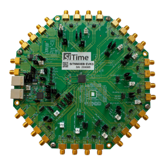
Page 34: Appendix B: Evb Top View
SiT6503EB Evaluation Board (EVB) HW User Manual Appendix B: EVB Top View CLK10_OUT CLK9_OUT CLK8_OUT CLK7_OUT CLK6_OUT Additional USB Power CLK5_OUT USB Cable from PC CLK4_OUT CLK3_OUT CLK0_OUT CLK1_OUT CLK2_OUT Figure B1. SiT6503EB Top View SiT6503EB HW UM Rev. 1.01 Page 34 of 35 www.sitime.com... - Page 35 © SiTime Corporation, November 2019. The information contained herein is subject to change at any time without notice. SiTime assumes no responsibility or liabi lity for any loss, damage or defect of a Product which is caused in whole or in part by (i) use of any circuitry other than circuitry embodied in a SiTime product, (ii) misuse or abuse...
Need help?
Do you have a question about the SiT6503EB and is the answer not in the manual?
Questions and answers