ICP DAS USA PCI-1202 Series Hardware User Manual
Hide thumbs
Also See for PCI-1202 Series:
- User manual (123 pages) ,
- Quick start manual (8 pages) ,
- User manual (123 pages)
Table of Contents
Advertisement
Quick Links
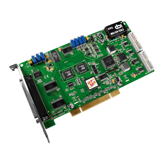
PCI-1202/1602/1800/1802
Warranty
All products manufactured by ICP DAS are warranted against defective materials for a
period of one year from the date of delivery to the original purchaser.
Warning
ICP DAS assume no liability for damages consequent to the use of this product. ICP
DAS reserves the right to change this manual at any time without notice. The information
furnished by ICP DAS is believed to be accurate and reliable. However, no responsibility is
assumed by ICP DAS for its use, nor for any infringements of patents or other rights of third
parties resulting from its use.
Copyright
Copyright © 1998~1999 by ICP DAS. All rights are reserved.
Trademark
The names used for identification only may be registered trademarks of their respective
companies.
Hardware User's Manual
Version: 4.4
(Dec.2009, PMH-014-42)
---- 1
Advertisement
Table of Contents

Related Manuals for ICP DAS USA PCI-1202 Series


Summary of Contents for ICP DAS USA PCI-1202 Series
- Page 1 PCI-1202/1602/1800/1802 Hardware User’s Manual Warranty All products manufactured by ICP DAS are warranted against defective materials for a period of one year from the date of delivery to the original purchaser. Warning ICP DAS assume no liability for damages consequent to the use of this product. ICP DAS reserves the right to change this manual at any time without notice.
-
Page 2: Table Of Contents
Table of Contents 1. INTRODUCTION .............................. 5 1.1 G ..........................5 ENERAL ESCRIPTION 1.2 T ..........................6 LOCK IAGRAMS 1.3 F ..............................7 EATURES 1.4 S ............................8 PECIFICATIONS 1.4.1 PCI-1202L/H/LU/HU..........................8 1.4.2 PCI-1602/1602F............................ 9 1.4.3 PCI-1800/1802 ............................ 10 1.4.4 Analog Input Range..........................11 1.4.5 A/D Trigger Methods .......................... - Page 3 3.5 S 2: T ........................36 ECTION IMER ONTROL 3.6 S 3: C ....................... 39 ECTION ONTROL EGISTER 3.6.1 The control register ..........................39 3.6.2 The status register ..........................60 3.6.3 The A/D software trigger register ....................... 61 3.7 S 4: D/I/O R ........................
- Page 4 9.1 P &P ........................98 OWER 9.2 D &P ........................98 RIVER 9.3 D/O T ..............................99 9.4 D/A T ..............................99 9.5 A/D T ..............................99 10. PERFORMANCE EVALUATION ......................100 PCI-1202/1602/1800/1802 Hardware User’s Manual (Ver.4.2, Dec/2009, PMH-014-42)---- 4...
-
Page 5: Introduction
1. Introduction 1.1 General Description The PCI-1800 and PCI-1802 are high performance, multifunction analog, digital (H/L) (H/L) I/O board for PC and compatible computers in a 5 V PCI slot. This series features a continuous, , gap-free data acquisition under DOS, Windows 95/98 and Windows NT 330 k Samples/Sec 3.51/4.0. -
Page 6: The Block Diagrams
1.2 The Block Diagrams The block diagram of PCI-1202/1602/1800/1802 is given as follows: X86 System EPROM PCI Interface System Status Local System Controller Control Digital Input 16 bits DI 16 bits DO Digital Output DAC OUT 0 2 channels 12 bit DA Converter DAC OUT 1 Analog Output... -
Page 7: Features
1.3 Features The general features of PCI-1202/1602/1800/1802 series are given as follows: * Bus: 5 V PCI ( Peripherals Component Interface) bus for PCI-1202/1602/180x H/L * Universal PCI card, supports both 5 V and 3.3 V PCI bus for PCI-1202HU/LU,1602U/FU * A/D: 1. -
Page 8: Specifications
1.4 Specifications 1.4.1 PCI-1202L/H/LU/HU Model Name PCI-1202 L PCI-1202 H PCI-1202 LU PCI-1202 HU Analog Input Channels 32 single-ended / 16 differential A/D Converter 12-bit, 8.5 µs conversion time Sampling Rate 110 kS/s. max. FIFO Size 1024 samples Over voltage Protection Continuous +/-35 Vp-p Input Impedance 10 MΩ/6 pF... -
Page 9: Pci-1602/1602F
1.4.2 PCI-1602/1602F Model Name PCI-1602 PCI-1602U PCI-1602 F PCI-1602 FU Analog Input Channels 32 single-ended / 16 differential AD Converter 16-bit, 2 µs conversion time Sampling Rate 100 kS/s. max. 200 kS/s. max. FIFO Size 8192 samples Over voltage Protection Continuous +/-35 Vp-p Input Impedance 10 MΩ/6 pF... -
Page 10: Pci-1800/1802
1.4.3 PCI-1800/1802 Model Name PCI-1802 H/L PCI-1800 H/L Analog Input Channels 32 single-ended / 16 differential 16 single-ended / 8 differential AD Converter 12-bit, 3 µs conversion time Sampling Rate 330 kS/s. max. FIFO Size 8192 samples 1024 samples Over voltage Protection Continuous +/-35 Vp-p Input Impedance 10 MΩ/6 pF... -
Page 11: Analog Input Range
1.4.4 Analog Input Range Model PCI-1202 L /PCI-1202 LU (Low-Gain) Gain +/- 10 +/- 5 +/- 2.5 +/- 1.25 +/- 0.625 Unipolar(V) 0 ~ 10 0 ~ 5 0 ~ 2.5 0 ~ 1.25 Bipolar(V) Sampling 110 kS/s Rate Max. Model PCI-1202 H / PCI-1202 HU (High-Gain) 1000... - Page 12 12-bit ADC Input Voltages and Output Codes for PCI-1202/1800/1802 H/L/HU/LU Analog Input Digital Output Binary Code Hex Code +9.995 V 1111 1111 1111 1000 0000 0000 -4.88 mv 0111 1111 1111 -10 V 0000 0000 0000 16-bit ADC Input Voltages and Output Codes for PCI-1602 /F/U/FU Analog Input Digital Output Binary Code Hex Code...
-
Page 13: A/D Trigger Methods
1.4.5 A/D Trigger Methods Trigger modes: 1. Internal software trigger 2. Internal pacer trigger 3. External trigger: pre-trigger, middle-trigger and post-trigger External trigger Start Start Internal pacer trigger External post-trigger External trigger External trigger Start Start External middle- External pre- Figure 1-2 Trigger modes of PCI-1202/1602/1800/1802 PCI-1202/1602/1800/1802 Hardware User’s Manual (Ver. -
Page 14: Applications
1.5 Applications Signal analysis. FFT & frequency analysis. Transient analysis. Speech analysis. Temperature monitor. Production test. Process control. Vibration analysis. Energy management. Other industrial and laboratory measurement and control. 1.6 Product Check List Your package includes the following items: One PCI-1202/1602/1800/1802 H/L/HU/LU multifunction card. One company CD One Quick Start Guide It is recommended to read the Quick Start Guide first. -
Page 15: Hardware Configuration
2. Hardware Configuration 2.1 Board Layout Figure 2-1 PCI-180X /NDA board layout (H/L) PCI-1202/1602/1800/1802 Hardware User’s Manual (Ver. 4.2, Dec/2009, PMH-014-42)---- 15... - Page 16 Figure 2-2 PCI-1202 /1800 /1802 board layout (H/L) (H/L) (H/L) PCI-1202/1602/1800/1802 Hardware User’s Manual (Ver.4.2, Dec/2009, PMH-014-42)---- 16...
- Page 17 Figure 2-3. PCI-1202 board layout (HU/LU) PCI-1202/1602/1800/1802 Hardware User’s Manual (Ver. 4.2, Dec/2009, PMH-014-42)---- 17...
- Page 18 O U T Figure 2-4 PCI-1602/1602F board layout PCI-1202/1602/1800/1802 Hardware User’s Manual (Ver.4.2, Dec/2009, PMH-014-42)---- 18...
- Page 19 O U T Figure 2-4 PCI-1602U/1602FU board layout PCI-1202/1602/1800/1802 Hardware User’s Manual (Ver. 4.2, Dec/2009, PMH-014-42)---- 19...
-
Page 20: Jumper Setting
2.2 Jumper Setting 2.2.1 JP1 : A/D Input Type Selection This jumper is used to select the analog input type. For single-ended inputs, the use should connect pin1, 3 and pin2, 4. For differential inputs, pin3, 5 and pin4, 6 should be connected. Differential Single-Ended Inputs... -
Page 21: Daughter Boards
2.3 Daughter Boards 2.3.1 DB-1825 The DB-1825 is a daughter board designed for 32 channels AD cards such as ISO_AD32, PCI-1202/1602/1802. Refer to Appendix A for “DB-1825 user manual". 37pin cable 2.3.2 DB-8225 The DB-8225 provides a on-board CJC(Cold Junction Compensation) circuit for thermocouple measurement and terminal block for easy signal connection and measurement. -
Page 22: Db-16P Isolated Input Board
2.3.5 DB-16P Isolated Input Board The DB-16P is a 16-channel isolated digital input daughter board. The optically isolated inputs of the DB-16P consists are bi-directional optocoupler with resistor for current sensing. You can use the DB-16P to sense DC signal from TTL levels up to 24 V or use the DB-16P to sense a wide range of AC signals. -
Page 23: Db-16R Relay Board
2.3.6 DB-16R Relay Board The DB-16R, 16-channel relay output board, consists of 16 from C relays for efficient switch of load by programmed control. It is connector and functionally compatible with 785 series board but with industrial type terminal block. The relay are energized by apply 5 voltage signal to the appropriated relay channel on the 20-pin flat connector. -
Page 24: Db-24Pr Power Relay Board
2.3.7 DB-24PR Power Relay Board The DB-24PR, 24-channel power relay output board, consists of 8 form C and 16 form A electromechanical relays for efficient switching of load programmed control. The contact of each relay can control a 5 A load at 250 V /30 V . -
Page 25: Analog Input Signal Connection
2.4 Analog Input Signal Connection The PCI-1202/1602/1800/1802 can measure single-ended or differential type analog input signal. Some analog signal can be measured in single-end or differential mode, but some analog signal only can be measured in one of the single-ended or differential mode. The user must decide which mode is suitable for measurement. - Page 26 Figure 2-4. Connecting to grounding source input (Right way) A/D CH0 HI Es 1 A/D CH 0 LO A.GND 1 A/D CH n HI Es n A/D CHn LO A.GND n Figure 2-4. Wrong way A/D CH0HI A/D CH0LO GND1 AGND A/D CHnHI A/D CHnLO...
- Page 27 Figure 2-5. Connecting to singled-ended input configuration PCI-1202/1602/1800/1802 A/D CH0 A/D CH1 A/D CH n AGND Figure 2-6. connecting to thermocouple configuration PCI-1202/1602/1800/1802 A/D CH 0 HI A/D CH 0 LO A/D CH n HI A/D CH n LO A. GND Do not join LO to A.GND at the computer Note : If the input signal is not thermocouple, the user should use oscilloscope to measure common mode voltage of Vin before connecting to PCI-1202/1602/1800/1802.
- Page 28 Figure 2-7. connecting to floating source configuration PCI-1202/1602/1800/1802 A/D CH 0 HI Es 1 A/D CH 0 LO A.GND A/D CH n HI Es n A/D CH n LO A.GND Signal Shielding Signal shielding connections in Figure 2-4 to Figure 2-7 are all the same Use single-point connection to frame ground (not A.GND or D.GND) PCI-1202/1602/1800/1802 A.GND...
-
Page 29: The Connectors
2.5 The Connectors CON1: Pin assignment of the digital output connector. Name Name Digital output 0 Digital output 1 Digital output 2 Digital output 3 Digital output 4 Digital output 5 Digital output 6 Digital output 7 Digital output 8 Digital output 9 Digital output 10 Digital output 11... - Page 30 C0N3: pin assignment of single-ended/differential input. (for PCI-1202/1602/1802H/L/HU/LU) Name Name Analog input 0/0+ Analog input 16/0- Analog input 1/1+ Analog input 17/1- Analog input 2/2+ Analog input 18/2- Analog input 3/3+ Analog input 19/3- Analog input 4/4+ Analog input 20/4- Analog input 5/5+ Analog input 21/5- Analog input 6/6+...
- Page 31 CON3: pin assignment of single-ended/differential input.(for PCI-1800H/L) Name Name Analog input 0/0+ Analog input 8/0- Analog input 1/1+ Analog input 9/1- Analog input 2/2+ Analog input 10/2- Analog input 3/3+ Analog input 11/3- Analog input 4/4+ Analog input 12/4- Analog input 5/5+ Analog input 13/5- Analog input 6/6+ Analog input 14/6-...
-
Page 32: I/O Control Register
3. I/O Control Register 3.1 How to Find the I/O Address The plug&play BIOS will assign a proper I/O address to every PCI-1800/1802 card in the power-on stage. The P180X_DriverInit(..) can detect how many PCI-1800/1802 cards in the system. Then the P180X_DriverInit(..) will detect the I/O address of these cards. The P180X_DriverInit(..) is supported in NAPPCI/dos, NAPPCI/w31, NAPPCI/w95 and NAPPCI/wnt. -
Page 33: The Assignment Of I/O Address
3.2 The Assignment of I/O Address The plug&play BIOS will assign the proper I/O address to PCI-1202/1602/1800/1802. If there is only one PCI-1202/1602/1800/1802, the user can identify the board_1. If there are two PCI-1202/1602/1800/1802 cards in the system, the user will be very difficult to identify which board is board_1. - Page 34 Section Address Name Operation Access Section1 + 0h PCI controller add-on 32-bit mail box Section1 + 38h PCI interrupt control 32-bit register Section1 + 3Ch On board NV-RAM 32-bit (or 3Eh, 3Fh) access control register (8-bit) Section2 + 00h 8254 timer1 8/16/32-bit Section2 + 04h 8254 timer2...
-
Page 35: Section 1: Pci Controller
3.4 Section 1: PCI Controller Although 64 I/O ports are used by on-board PCI-controller, only 3 registers can be directly used by user. Address Access Functions Operation Write only Out-going mail-box Write a 0 to wait for add-on (32-bit) interrupt. Enable : Write 00010010h to this port. -
Page 36: Section 2: Timer Control
3.5 Section 2: Timer Control The timer-0 is used as the internal trigger A/D pacer timer. The timer-1 is designed for the external trigger pacer timer. The timer-2 is used as the machine independent timer. The timer- 2 is very important for settling time delay. Refer to Intel's “Microsystem Components Handbook"... - Page 37 // timer0 for pacer trigger void enable_timer0(WORD divv) // for internal pacer trigger outport((WORD)(wAddrTimer+3*4), 0x34); /* enable pacer timer_0 */ outport((WORD)(wAddrTimer+0*4), (WORD)(divv & 0xff)); outport((WORD)(wAddrTimer+0*4), (WORD)((divv>>8) & 0xff)); void disable_timer0(void) outport((WORD)(wAddrTimer+3*4), 0x34); /* disable pacer timer_0 */ outport((WORD)(wAddrTimer+0*4), 0x01); outport((WORD)(wAddrTimer+0*4), 0x00); // timer1 for external trigger void enable_timer1(WORD divv)
- Page 38 // timer2 for Machine Independent Timer /* address of timer 2 = wAddrTimer+2*4 address of ctrl = wAddrTimer+3*4 input clock = 8 M down count 8 time = 1 μs down count 65536/8 = 8192 μs --> max 8191 μs WORD P180X_DelayUs(WORD wDelayUs) WORD wDownCount,wLow,wHigh,wVal;...
-
Page 39: Section 3: Control Register
3.6 Section 3: Control Register I/O address of control register = wAddrCtrl + 0*4 I/O address of status register = wAddrCtrl + 0*4 I/O address of trigger register = wAddrCtrl + 1*4 The flow path of analog input signal is given as follows: Signals Max=+/-10V Max=+/-5V... - Page 40 3.6.1.1 Bit4~ Bit0: A/D channel select A/D channel 1800/1202/1602/1802 1800/1202/1602/1802 1202/1602/1802 1202/1602/1802 3.6.1.2 Gain control [B7, B6] PCI-1XXX L/LU PCI-1XXX H/HU [0, 0] PGA=1 PGA=1 [0, 1] PGA=2 PGA=10 [1, 0] PGA=4 PGA=100 [1, 1] PGA=8 PGA=1000 3.6.1.3 Input range control [B9, B8] Output [0, 0]...
- Page 41 3.6.1.4 Configuration Table The configuration table of PCI-1202L/LU/1800L/1802L is given as follows: Bipolar/Unipolar Input Signal Range Gain Settling Time [B9,B8,B7,B6] Bipolar +/- 5 V 3 μs 0000 Bipolar +/- 2.5 V 3 μs 0001 Bipolar +/- 1.25 V 3 μs 0010 Bipolar +/- 0.625 V...
- Page 42 3.6.1.5 Set Channel Configuration The demo program to set the channel/gain is given as follows: WORD P180X_SetChannelConfig(WORD wAdChannel, WORD wAdConfig) WORD wConfig,wChannel; wChannel = (wAdChannel&0x1f); wSysConfig = (wAdConfig&0x1f); // store for P1802_AdPolling wConfig = (wAdConfig&0x0f); wConfig = wConfig << 6; wConfig += wChannel;...
- Page 43 3.6.1.6 Calculate the A/D Value The demo program to calculate the real A/D value is given as follows: double ComputeRealValue(DWORD dwAdConfig, DWORD dwAdHex) WORD wZERO; double dfMAX, dfVal; switch (dwAdConfig) case 0 : wZERO=2048; dfMAX=5.0; break; case 1 : wZERO=2048; dfMAX=2.5; break;...
- Page 44 3.6.1.7 Command Sets of MagicScan Controller The command sets of MagicScan controller are given as follows: Command [B12~B10] Descriptions Reset [0 0 0] Reset the MagicScan controller. The software driver must send this command once after power-on. Set channel/gain [0 0 1] Set the channel/gain value of the fixed-channel mode.
- Page 45 The demo program of send command to MagicScan control is given as follows: WORD pic_control(WORD i) WORD j; if ((inport(wAddrCtrl)&0x04)==0) outport(wAddrCtrl,0xffff); /* send a recovery to PIC */ j=0; while ((inport(wAddrCtrl)&0x04)==0) j++; if (j>65530) return(AdControllerError); /* time out */ i = i & 0xDFFF; /* set pic low !! */ outport(wAddrCtrl,i);...
- Page 46 The demo program to set the channel/gain is given as follows: WORD P180X_SetChannelConfig(WORD wAdChannel, WORD wAdConfig) WORD wConfig,wChannel; wChannel = (wAdChannel&0x1f); wSysConfig = (wAdConfig&0x1f); // store for P1802_AdPolling wConfig = (wAdConfig&0x0f); wConfig = wConfig << 6; wConfig += wChannel; /* Bit15=1 --> no reset FIFO Bit14=? Bit13=? Bit12=0 -->...
- Page 47 The demo program to add to MagicScan queue is given as follows: WORD P180X_AddToScan(WORD wAdChannel, WORD wAdConfig, WORD wAverage, WORD wLowAlarm, WORD wHighAlarm, WORD wAlarmType) {WORD wConfig,wChannel,wRetVal; if (wAlarmType>=5) return(AlarmTypeError); wMagicLowAlarm[wMP]=wLowAlarm; wMagicHighAlarm[wMP]=wHighAlarm; wMagicAlarmType[wMP]=wAlarmType; wChannel = wAdChannel&0x1f; wMagicChannel[wMP]=wChannel; wSysConfig = wAdConfig&0x1f; /* Store for P180X_AdPolling */ wMagicConfig[wMP]=wSysConfig;...
- Page 48 The demo program to start MagicScan operation is given as follows: WORD P180X_StartScan(WORD wSampleRate, WORD wNum) WORD wVal; WORD wRetVal; wMagicNum=wNum; disable_timer0(); /* Disable pacer timer first */ /* start MagicScan controller */ wRetVal=pic_control(0xD400); /* 11?1 01?? ???? ???? cmd_101=start scan */ if (wRetVal!=0) return(wVal);...
- Page 49 3.6.1.8 External Trigger Control The operation steps of post-trigger are given as follows: Step 1: Disable all external trigger External trigger signal Step 2: Set the pacer rate of timer-1 Step 3: Clear FIFO & disable timer-1 Step4: Wait until external trigger signal to enable timer-1 Step 5: Fetch N data(N=End-Start) Start...
- Page 50 The software flowchart of external trigger operation is given as follows: P180X_ClearScan Clear the MagicScan controller Add channel 1 to circular queue P180X_AddToScan If the AD data need to save P180X_SaveScan Add channel 2 to circular queue P180X_AddToScan P180X_SaveScan If the AD data need to save P180X_AddToScan Add channel ? to circular queue P180X_SaveScan...
- Page 51 The demo program of post-trigger is given as follows: wRetVal=P180X_ClearScan(); wRetVal += P180X_AddToScan(0,0,1,0,0,0); // CH:0 to scan wRetVal += P180X_SaveScan(0,wV0); wRetVal += P180X_AddToScan(2,0,1,0,0,0); // CH:2 to scan wRetVal += P180X_SaveScan(1,wV2); // Notice: 1 not 2 ^ : This is a ordinal number in // Scan Queue not a channel number.
- Page 52 The B13 must set to 1 to set the external trigger logic. The external trigger controller commands are given as follows: Trigger Command sequences Descriptions [B12, B11, B10 ] Disable external trigger [ 1, 0, X] Disable all external trigger. (for PCI-1800/1X02) [ 1, 0, X] disable all external trigger...
- Page 53 The Windows driver of post-trigger is given as follows: WORD CALLBACK P180X_StartScanPostTrg(WORD wSampleRateDiv, DWORD dwNum, SHORT nPriority) disable_timer0(); // disable internal pacer timer disable_timer1(); // disable external pacer timer wVal=pic_control(0xD400); /* 11?1 01?? ???? ???? cmd_101=start scan */ if (wVal!=0) return(wVal); _outpw(wAddrCtrl,0xf000);...
- Page 54 The windows driver of pre-trigger is given as follows: WORD CALLBACK P180X_StartScanPreTrg(WORD wSampleRateDiv, DWORD dwNum, SHORT nPriority) disable_timer0(); // disable internal pacer timer disable_timer1(); // disable external pacer timer wVal=pic_control(0xD400); /* 11?1 01?? ???? ???? cmd_101=start scan */ if (wVal!=0) return(wVal); _outpw(wAddrCtrl,0xf000);...
- Page 55 The windows driver of middle-trigger is given as follows: WORD CALLBACK P180X_StartScanMiddleTrg(WORD wSampleRateDiv, DWORD dwNum, SHORT nPriority) disable_timer0(); // disable internal pacer timer disable_timer1(); // disable external pacer timer wVal=pic_control(0xD400); /* 11?1 01?? ???? ???? cmd_101=start scan */ if (wVal!=0) return(wVal); _outpw(wAddrCtrl,0xf000);...
- Page 56 The pre-trigger driver for PCI-1800/1802/ver-C is given as follows: WORD CALLBACK P180X_StartScanPreTrgVerC(WORD wSampleRateDiv, DWORD dwNum, SHORT nPriority) disable_timer0(); // disable internal pacer timer disable_timer1(); // disable external pacer timer wVal=pic_control(0xD400); /* 11?1 01?? ???? ???? cmd_101=start scan */ if (wVal!=0) return(wVal); _outpw(wAddrCtrl,0xf000);...
- Page 57 The middle-trigger driver for PCI-1800/1802/ver-C is given as follows: WORD CALLBACK P180X_StartScanMiddleTrgVerC(WORD wSampleRateDiv, DWORD dwNum, SHORT nPriority) disable_timer0(); // disable internal pacer timer disable_timer1(); // disable external pacer timer wVal=pic_control(0xD400); /* 11?1 01?? ???? ???? cmd_101=start scan */ if (wVal!=0) return(wVal); _outpw(wAddrCtrl,0xf000);...
- Page 58 The external trigger drivers are given as follows: Driver Name demo Applications program P180X_StartScanPostTrg(…) demo23.c for PCI-1800/1802 ver-C & ver-F P180X_StartScanPreTrg(…) demo24.c for PCI-1800/1802 ver-F P180X_StartScanMiddleTrg(…) demo25.c for PCI-1800/1802 ver-F P180X_StartScanPreTrgOld(…) demo26.c for PCI-1800/1802 ver-C P180X_StartScanMiddleTrgOld(…) demo27.c for PCI-1800/1802 ver-C P1202_StartScanPostTrg(…) demo23.c for PCI-1202...
- Page 59 3.6.1.10 Handshake Control Bit Set the B13 to 0 if the command is sent to the MagicScan controller. Keep this bit at high when not used. The demo program of handshaking is given as follows: WORD pic_control(WORD i) WORD j; if ((inport(wAddrCtrl)&0x04)==0) outport(wAddrCtrl,0xffff);...
-
Page 60: The Status Register
3.6.2 The status register The format of the status register is given as follows: Bit7 Bit6 Bit5 Bit4 Bit3 Bit2 Bit1 Bit0 Bit 7: FIFO half-full FIFO is half-full. Bit 6: FIFO full FIFO is full. Bit 5: FIFO empty FIFO is empty. -
Page 61: The A/D Software Trigger Register
3.6.3 The A/D software trigger register Writing to this port will perform a software trigger signal to trigger an A/D conversion. Although the PC can send very fast trigger signal (more than 333 k ), the max. sampling rate of A/D conversion can not over 330 k Samples/Sec.. -
Page 62: Section 4: D/I/O Register
3.7 Section 4: D/I/O Register 3.7.1 Digital Output/Digital Input I/O address of D/I = wAddrDio I/O address of D/O = wAddrDio The PCI-1800/1802 provides 16-channel digital input and 16-channel digital output. All levels are TTL compatible. The connections diagram and block diagram are given below: CON2 I/O read signal. -
Page 63: Card Id Register
The demo program of D/I/O is given as follows: WORD P180X_Di(WORD *wDi) P1202_Di(…) for PCI-1202 P1602_Di(…) for PCI-1602 *wDi=inport(wAddrDio)&0xffff; return(NoError); WORD P180X_Do(WORD wDo) P1202_Do(…) for PCI-1202 P1602_Do(…) for PCI-1602 outport(wAddrDio,wDo); return(NoError); 3.7.2 Card ID Register The format of the Card_ID register is given as follows: X Bit3 Bit2 Bit1 Bit0 It can read card ID set from switch (SW1) The demo program of card ID is given as follows:... -
Page 64: Section 5: A/D & D/A Register
3.8 Section 5: A/D & D/A Register I/O address of DA-0 = wAddrAdda I/O address of DA-1 = wAddrAdda + 1*4 I/O address of FIFO = wAddrAdda Writing data to this section will write data to the DACs and reading data from this port will read the data from A/D FIFO. - Page 65 The demo program for D/A is given as follows: WORD P180X_Da(WORD wDaChannel, WORD wDaVal) P1202_Da(…) for PCI-1202 if (wDaChannel==0) /* channel 0 */ P1602_Da(…) for PCI-1602 outport(wAddrAdda,wDaVal); return(NoError); else if (wDaChannel==1) /* channel_1 */ outport((wAddrAdda+4),wDaVal); return(NoError); else return(DaChannelError); The demo program of software trigger A/D conversion is given as follows: WORD P180X_AdPollingHex(Word *AdVal) P1202_AdPollingHex(…) for PCI-1202 WORD...
-
Page 66: A/D Conversion Operation
4. A/D Conversion Operation 4.1 The Configuration Code Table PCI-1202L/1202LU/1800L/1802L Configuration Code Table Bipolar/Unipolar Input Signal Range Gain Settling Time Configuration Code Bipolar +/- 5 V 3 μs 0x00 Bipolar +/- 2.5 V 3 μs 0x01 Bipolar +/- 1.25 V 3 μs 0x02 Bipolar... -
Page 67: The Unipolar/Bipolar
PCI-1202H/1202HU/1800H/1802H Configuration Code Table Bipolar/Unipolar Input Signal Range Gain Settling Time Configuration Code Bipolar +/- 5 V 23 μs 0x10 Bipolar +/- 0.5 V 28 μs 0x11 Bipolar +/- 0.05 V 140 μs 0x12 Bipolar +/- 0.005 V 1000 1300 μs 0x13 Bipolar +/- 10 V... -
Page 68: The Settling Time
4.4 The Settling Time If the channel number or gain factor is changed, the hardware need extra time for signal ready. This is called the settling time. This limitation will apply both to the Fixed- channel mode and MagicScan mode AD conversions. So the user must take care to avoid the settling error. -
Page 69: The Ad Conversion Mode
4.6 The AD Conversion Mode The AD conversion operation of PCI-1202/1602/1800/1802 can be divided into two different mode: Fixed-channel mode and the MagicScan mode. • The functions of fixed-channel mode are given as follows: 1. P180X_SetChannelConfig The reading data is in 2. - Page 70 • The functions of continuous capture with storing data to main memory are given as follows: (two board operating simultaneously) 1. P180X_FunA_Start 2. P180X_FunA_ReadStatus 3. P180X_FunA_Stop 4. P180X_FunA_Get • The functions of continuous capture with storing data to main memory are given as follows: (single board operating) 1.
-
Page 71: The Fixed-Channel Mode Ad Conversion
The Fixed-channel Mode AD Conversion The P180X_SetChannelConfig will active the selected channel and its configuration code. Then the other functions will refer to that channel and configuration. The general flow chart is given as follows : P180X_SetChannelConfig Select the active channel 1 P180X_DelayUs Delay the settling time (if needed) Perform one AD conversion... -
Page 72: The Magicscan Mode Ad Conversion
The MagicScan Mode AD Conversion The P180X_ClearScan will set the MagicScan controller to its initial state. The P180X_AddToScan will add the channels to MagicScan circular queue one by one. The order of P180X_AddToScan is the scan order. The maximum queue size is 48. The scan order is random and can be repeat. -
Page 73: The Magicscan Circular_Scan_Queue
4.8.1 The MagicScan Circular_Scan_Queue The MagicScan controller equips a circular queue for scan sequence control. The scan sequence is one by one and repeatable with the limitation of maximum 48 channels. So the following scan sequence are all validate : One channel MagicScan Two channels MagicScan, scan Two channels MagicScan, scan... -
Page 74: The Digital Filter Of Magicscan
4.8.2 The Digital Filter of MagicScan The digital filter is a average filter. Filter value = (V_1+V_2+……+V_n)/n, where n is average factor If the input signal is very noisy, this filter can be used to remove these noises. 4.8.3 The Different Sampling Rate of MagicScan The MagicScan controller scans the analog inputs in fixed-sampling-rate. -
Page 75: The High/Low Alarm Of Magicscan
4.8.4 The High/Low Alarm of MagicScan There are 5 alarm types are given as follows: Type 0 : no alarm Type 1 : high alarm any AD data > High_alarm_value Type 2 : low alarm any AD data < Low_alarm_value Type 3 : in alarm Low_alarm_value <... -
Page 76: The Magicscan Function
4.8.5 The MagicScan Function The features of MagicScan are given as follows: 1. Different gain for each channel 2. Non-sequential order for channel scan 3. Different sampling rate for each channel (use with digital filter) 4. Programmable different digital filter for each scan channel 5. - Page 77 The A/D conversion data in FIFO are in the same sampling rate (refer to (1), (2), (3)). For example, the scan channel is 1 the pacer sampling rate is 330 k the expected sampling rate for channel 1 is 110 k the expected sampling rate for channel 2 is 55 k the expected sampling rate for channel 3 is 11 k The hardware will scan the analog data into FIFO as follows:...
-
Page 78: The Magicscan Thread
4.8.6 The MagicScan Thread //---------------------------------------------------------------------- // wThreadStatus : 0x01=MagicScan start 0x02=timeout1 0x04=timeout2 0x08=FIFO overflow 0x80=MagicScan OK WORD magic_scan() WORD wVal,w1,w3; DWORD i,dwTime,j,k,dwIndex; for (j=0; j<wMP; j++) dwMagicSum[j]=0; for (j=0; j<wMP; j++) wMagicNow[j]=wMagicAve[j]; for (j=0; j<wMP; j++) wMagicP[j]=0; for (i=0; i<wMP; i++) // skip the MagicScan settling time dwTime=0;... - Page 79 for (;;) wVal=inport(wAddrCtrl)&0x60; if (wVal==0x20) return FifoOverflow; if (wVal==0x60) break; dwTime++; if (dwTime>100000) return TimeOut; dwMagicSum[j]+=(inport(wAddrAdda)&0x0fff); /* 0x0fff for 12-bitADC, 0xffff for 16-bit ADC */ wMagicNow[j]--; w1=wMagicNow[j]; if (w1==0) wVal=(WORD)(dwMagicSum[j]/wMagicAve[j]); if (wMagicScanSave[j]==1) *((wMagicScanBuf[j])+wMagicP[j])=wVal; wMagicP[j]++; w3=wMagicAlarmType[j]; if(w3>0) // 0 = no alarm dwIndex=0x01;...
- Page 80 if (wVal<wMagicLowAlarm[j]) dwMagicLowAlarm |= dwIndex; if (wVal>wMagicHighAlarm[j]) dwMagicHighAlarm |= dwIndex; else if (w3==3) // 3 = in [low,high] alarm if ((wVal>wMagicLowAlarm[j])&& (wVal<wMagicHighAlarm[j])) dwMagicLowAlarm |= dwIndex; dwMagicHighAlarm |= dwIndex; dwMagicSum[j]=0; wMagicNow[j]=wMagicAve[j]; } // end if(w1 } // end for(j= } // end for(i= ret_label: disable_timer0();...
-
Page 81: M_Function
5. M_Function Some real world applications have to send out the pre-defined pattern to the external device and measure the output responses for analysis. The user need one arbitrary wave form generator and one high speed A/D converter. The M_Functions, provided by PCI- 1202/1602/1800/1802, can send out the user defined arbitrary waveform and perform the A/D conversion at the same time. -
Page 82: Introduction
5.1 Introduction What Is M_Functions? The features of the M_Functions are given as follows: 1. Arbitrary wave form generation from D/A output port (2 channels max.) 2. Perform MagicScan A/D conversion at the same time (32 channels max.) 3. Only one function call is needed 4. - Page 83 Figure 5-3: The M_Function_1 send out a 100 k, +/-5 V sine wave. (measured by Tektronix TDS 220) Figure 5-4: The M_Function_1 send out a 200 k, +/-5 V sine wave. (measured by Tektronix TDS 220) PCI-1202/1602/1800/1802 Hardware User’s Manual (Ver.
- Page 84 How many M_Functions are ready now ? There are four M_Functions, P180X_M_FUN_1, P180X_M_FUN_2, P180X_M_FUN_3 and M_FUN_4 are ready now. The M_FUN_1 will automatic to compute the sine wave output image. The M_FUN_2 is designed for arbitrary waveform generation, so the user can prepare their waveform for M_FUN_2.
- Page 85 Limitation The system will interrupt the driver software under Windows 95/NT. The partial function of D/A arbitrary waveform generation is implemented by software. Therefore the D/A output waveform will be distorted sometimes. Refer to Figure 5-5 for details. If the user has to generate the periodic wave form such as sin, cos …, and the analysis is similar to spectrum analysis, this type of output distortion will cause little trouble.
-
Page 86: Continuous Capture Functions
6. Continuous Capture Functions The continuous capture functions are very useful in real world applications. It can be used many types of applications. Those applications are 1. Low speed, no storage, real-time processing, continuous capture 2. High speed, store the A/D data in PC main memory, time is limited by memory size (Referring to P180X_FunA series functions and P180X_FunB series function for more Detail information in 6.2) 3. - Page 87 The block diagram of continuous capture function is given as follows: Magic Scan Card?_StartScan(...) Buffer Controller Analog FIFO Signal Converter Pacer Trigger Card?_ReadData(...) Timer Figure 6-1: The block diagram of continuous capture. The P180X_Card?_StartScan(…) will perform the follows function: 1. setup scan-queue 2.
- Page 88 • The sample program for single board is given as follows: wRetVal=P180X_Card0_StartScan(……); // setup continuous capture function // this function will create thread if (wRet != NoError) Show error message & return // now the thread is active and the continuous capture function is going now for(;;) wRetVal=P180X_Card0_ReadStatus(…);...
- Page 89 wRetVal=P180X_Card0_ReadStatus(….); if(wRetVal != 0) show these A/D data or save these A/D data or analyze these A/D data wRetVal=P180X_Card1_ReadStatus(….); if (wRetVal != 0) show these A/D data or save these A/D data or analyze these A/D data wRetVal=P180X_Card?_ReadStatus(….); if (wRetVal != 0) show these A/D data or save these A/D data or analyze these A/D data...
-
Page 90: Save Data In Pc Memory Driver
6.2 Save Data in PC Memory Driver The P180X_FunA & P180X_FunB are series functions designed for continuous capture which storing the data into main memory. The features for these P180X_FunA and P180X_FunB are listed as follows: Sampling A/D data with high speed (for example, 330K) Continues capture for a long period (for example, 2.5 minutes continue) A/D data save in the PC memory first, then analyze these data later (memory size=330 k*60*2.5=330 k*150=49.5 M word=99 M bytes) - Page 91 Figure 6-2. The Continuous Capture example. PCI-1202/1602/1800/1802 Hardware User’s Manual (Ver. 4.2, Dec/2009, PMH-014-42)---- 91...
-
Page 92: Calibration
7. Calibration 7.1 AD Calibration For PCI-1202/1800/1802 Step 1: Apply 0 V to channel 0 Step 2: Apply 4.996 V to channel 1 Step 3: Apply +0.6245 V to channel 2 for PCI-1202 /1800 /1802 (L/LU) Step 4: Apply +4.996 mV to channel 2 for PCI-1202 /1800 /1802 (H/HU) - Page 93 For PCI-1602/1602F/1602U/1602FU Step 1: Apply 0 V to channel 0 Step 2: Apply 4.996 V to channel 1 Step 3: Apply +0.6245 V to channel 2 Step 4: Run DEMO19.EXE Step 5: Adjust VR3 until channel 0 = 0000 or FFFF Step 6: Adjust VR2 until channel 1 = 7FFF or 7FFE Step 7: Repeat Step5 &...
-
Page 94: D/A Calibration
7.2 D/A Calibration • For PCI-1800/1802 version_F & PCI-1202 Step 1: J1 select +10 V Step 2: Connect the D/A channel 0 to voltage meter Step 3: Send 0x800 to D/A channel 0 Step 4: Adjust VR200 until voltage meter = 0 V Step 5: Send 0 to D/A channel 0 Step 6: Adjust VR201 until voltage meter = -10 V Step 7: Connect the D/A channel 1 to voltage meter... - Page 95 • For PCI-1800/1802 version_C Step 1: J1 select +10 V Step 2: Connect the D/A channel 0 to voltage meter Step 3: Send 0 to D/A channel 0 Step 4: Adjust VR3 until voltage meter = -10 V For PCI-1602 Step 1: J1 select +10 V Step 2: Connect the D/A channel 0 to voltage meter Step 3: Send 0x800 to D/A channel 0...
-
Page 96: Software And Demo Program
8. Software and Demo Program The software drivers can be classified as follows: for DOS: huge and large mode library for TC, MSC and BC for Windows: DLLs for VC++, BC++, VB, Delphi, BCB, LabVIEW There are about 20 demo program given as follows: demo1: one board, D/I/O test, D/A test, A/D polling test, general test demo2: two board, same as demo1 demo3: one board, A/D by software trigger(polling) and A/D by pacer trigger demo... - Page 97 demo28: multi-task, critical section driver demo demo29: testing for MagicScan controller. demo30: testing for Pacer Trigger. Demo31: testing for Polling. Demo32: monitoring the incoming data from MagicScan, then set a digital out bit on when the incoming data exceed a defined threshold. Demo33: MagicScan total sample rate=176 k/sec for 8 channels.
-
Page 98: Diagnostic Program
9. Diagnostic Program 9.1 Power-on Plug&Play Test The operation steps of power-on plug&play test are given as follows: Step 1: Power-off PC Step 2: Install PCI-1202/1602/1800/1802 without any extra external connector Step 3: Power-on PC and check the PC screen very carefully Step 4: The PC will performance self-test first Step 5: Detect the non-PCI physical devices installed in the system Step 6: Show the information of these device in screen... -
Page 99: D/O Test
9.3 D/O Test Step 1: Power-off PC Step 2: Install one PCI-1202/1602/1800/1802 card with a 20-pin flat cable between CON1 & CON2 Step 3: Power-on PC, run DEMO15.EXE Step 4: Check the value of D/O and D/I must be the same. 9.4 D/A Test Step 1: Power-off PC Step 2: Install one PCI-1202/1602/1800/1802 card with DA channel 0 connected to A/D... -
Page 100: Performance Evaluation
10. Performance Evaluation Demo Program Performance Description DEMO16.EXE. 1.7 MS/s D/I performance DEMO16.EXE. 2.1 MS/s D/O performance DEMO16.EXE. 2.0 MS/s D/A performance DEMO13.EXE 20 kS/s Continuous capture function, one card, two channels Total=20 kS/s 10 kS/s per channels DEMO14.EXE 20 kS/s Continuous capture function, two card, two channels Total=20 kS/s 10 kS/s per channels... - Page 101 Appendix A : The DB-1825 user manual A.1 : PCB layout for connecting to ISO_AD32: For differential input (R=0 ohm) DB-1825 Agnd 14- 14+ Agnd 12- 12+ Agnd 10- 10+ Agnd 8- Agnd Agnd Dgnd Agnd 15- 15+ Agnd 13- 13+ Agnd 11- 11+ Agnd 9- +5 V Agnd Extrg...
- Page 102 A.2 : PCB layout for connecting to PCI-1002/1202/1602/1802: For differential input (R=0 ohm) DB-1825 Agnd 14- 14+ Agnd 12- 12+ Agnd 10- 10+ Agnd 8- Agnd Agnd Dgnd Agnd 15- 15+ Agnd 13- 13+ Agnd 11- 11+ Agnd 9- DA1 DA2 Etrg Agnd 7- Agnd 5- Agnd 3-...
- Page 103 A.3 : connection to ISO-AD32 37pin cable A.4 : connection to PCI-1002/1202/1602/1802 37pin cable A.5 : connection to PCI-1x02 and multiple DB-889D(16 channels differential) 37pin cable 37pin cable 20 pins flat cable PCI-1202/1602/1800/1802 Hardware User’s Manual (Ver. 4.2, Dec/2009, PMH-014-42)---- 103...
Need help?
Do you have a question about the PCI-1202 Series and is the answer not in the manual?
Questions and answers