JVC TH-A10 Service Manual
Dvd digital theater system
Hide thumbs
Also See for TH-A10:
- Instructions manual (128 pages) ,
- Errata (1 page) ,
- Service manual (116 pages)
Table of Contents
Advertisement
Quick Links
SERVICE MANUAL
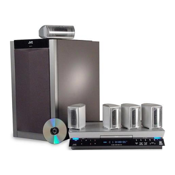
DVD DIGITAL THEATER SYSTEM
SP-PWA10
(DVD player)/XV-TH-A10
SP-THA10
TH-A10
(Speaker section)
Contents
Safety precautions
Preventing static electricity
Dismantling and assembling
the traverse unit
Disassembly method
COPYRIGHT
TH-A10
XV-THA10
SP-XSA10
SP-XCA10
SP-PWA10 (Powered subwoofer)
SP-XCA10 (Center speaker)
SP-XSA10 (Satellite speaker) x 4
1-2
1-3
1-4
1-5
2001 VICTOR COMPANY OF JAPAN, LTD.
SP-XSA10
3U
4U
Disassembly method
Main adjustment
Precautions for service
Description of major ICs
TH-A10
Area Suffix
TH-A10
Maiaysia, Thailand,
Philippines
Brazil, Mexico, Peru
1-17
1-21
1-24
1-25
No.20890
JAN. 2001
Advertisement
Table of Contents

Related Manuals for JVC TH-A10


Summary of Contents for JVC TH-A10
- Page 1 TH-A10 SP-PWA10 XV-THA10 SP-XSA10 SP-XSA10 SP-XCA10 Area Suffix TH-A10 Maiaysia, Thailand, Philippines Brazil, Mexico, Peru (DVD player)/XV-TH-A10 SP-PWA10 (Powered subwoofer) SP-THA10 TH-A10 SP-XCA10 (Center speaker) (Speaker section) SP-XSA10 (Satellite speaker) x 4 Contents Safety precautions Disassembly method 1-17 Preventing static electricity...
-
Page 2: Safety Precautions
TH-A10 Safety precautions 1. This design of this product contains special hardware and many circuits and components specially for safety purposes. For continued protection, no changes should be made to the original design unless authorized in writing by the manufacturer. -
Page 3: Preventing Static Electricity
TH-A10 Preventing static electricity Electrostatic discharge (ESD), which occurs when static electricity stored in the body, fabric, etc. is discharged, can destroy the laser diode in the traverse unit (optical pickup). Take care to prevent this when performing repairs. 1.1. Grounding to prevent damage by static electricity Static electricity in the work area can destroy the optical pickup (laser diode) in devices such as DVD players. -
Page 4: Dismantling And Assembling The Traverse Unit
TH-A10 Dismantling and assembling the traverse unit 1. Notice regarding replacement of optical pickup Electrostatic discharge (ESD), which occurs when static electricity stored in the body, fabric, etc. is discharged, can destroy the laser diode in the traverse unit (optical pickup). Take care to prevent this when performing repairs to the optical pickup or connected devices. -
Page 5: Disassembly Method
TH-A10 Disassembly method Top cover <Main body> Removing the top cover (See Fig.1 and 2) Remove the four screws A attaching the top cover (Use an Allen wrench). Joints a Lift up the front part of the top cover to release the two joints a and remove the top cover toward the front. -
Page 6: Removing The Front Panel Assembly
TH-A10 Removing the front panel assembly (See Fig. 6 to 9) Prior to performing the following procedure, remove the top cover, the rear cover and the side covers. Disconnect the harness from connector CN802 on the main board on the upper side of the body. -
Page 7: Removing The Rear Panel
TH-A10 Removing the right and left corner covers (See Fig.10 and 11) Prior to performing the following procedure, remove the top cover, the rear cover, the side covers and the front panel assembly. It is not necessary to remove the front panel assembly. - Page 8 TH-A10 Removing the DVD servo control board Analog I / O board Digital I / O board (See Fig.15 to 17) CN681 CN201 Prior to performing the following procedure, remcover and the right side cover.ove the top cover, the rear Remove the three screws G and pull the DVD servo control board case upward.
- Page 9 TH-A10 Removing the analog I / O board / the Analog I / O board Digital I / O board digital I / O board (See Fig.18 and 19) CN681 CN201 Prior to performing the following procedure, remove the top cover and the rear cover.
-
Page 10: Removing The Power Board
TH-A10 DVD mechanism cover Removing the DVD mechanism assembly (See Fig.22 and 23) Prior to performing the following procedure, remove the top cover, the rear cover, the front panel assembly, the DVD servo control board case, the analog I / O board, the digital I / O board and the tuner board. -
Page 11: Removing The Power Switch Board
TH-A10 Removing the power transformer assembly Rear panel (See Fig.24 and 25) Prior to performing the following procedures, remove the top cover and the rear cover. Disconnect the harnesses from connector CN911 and CN912 on the power board. Fig.24 Remove the two screws M attaching the power transformer assembly. - Page 12 TH-A10 Removing the eject board (See Fig.28) Eject board Switch board Disconnect the harness from connector CN702 on the eject board. Remove the three screws P attaching the eject board. CN702 Removing the LCD board (See Fig.29) Remove the four screws Q attaching the LCD board.
- Page 13 TH-A10 Loading tray <Removing DVD mechanism unit> Removing the clamper base (refer to Figure 1) o Remove the top cover. o Remove the DVD mechanism unit. 1. Remove the two screws at A fixing the clamper base. Clamper base Removing the loading tray (refer to Figures 2 - 4) o Remove the clamper base.
- Page 14 TH-A10 Traverse mechanism unit Removing the traverse mechanism unit (refer to Figure 5) o Remove the loading tray. 1. Remove the three screws at B fixing the traverse mechanism unit. Protecting the optical pickup o Solder the flexible ground point on the optical pickup when replacing the pickup or before detaching the mechanism control board.
- Page 15 TH-A10 Traverse chassis Removeing the turntable and spindle motor assemby (refer to Figures 8 - 9) o Remove the traverse mechanism unit. o Solder the flexible ground point on the optical pickup. (Figure 6) o Remove the mechanism control board.
- Page 16 TH-A10 Loading base Lever Removeing the loading mechanism parts (refer to Figures 10 - 11) o Remove the clamper base. Up-down cam o Remove the disk tray. Pawl A 1. Turn the lever counterclockwise until it stops (position 1), while pushing the switch lever in the direction of the arrow and pushing up the pawl at A using a screwdriver.
- Page 17 TH-A10 Disassembly method <Speaker> Amplifier assembly Removing the amplifier assembly (See Fig.1) Remove the twelve screws A attaching the amplifier assembly on the back of the body. Move the amplifier assembly backward and disconnect the harness from connector CN109 in the lower part of the amplifier assembly.
- Page 18 TH-A10 Removing the preamplifier board Main amplifier board Amplifier assembly (See Fig.4 to 6) Prior to performing the following procedure, remove the heat sink cover and the amplifier cover. Braket Remove the two screws E attaching the preamplifier Heat sink board to the bracket.
- Page 19 TH-A10 Removing Power Amplifier Board(See Fig.7 and 8) Prior to performing the following procedure, remove the heat sink cover, the amplifier cover, the preamplifier board and the power spply & SP terminal board. Disconnect the harness from connector CN104 on the power amplifier board.
- Page 20 TH-A10 Removing the power amplifier board (B) Joint c (See Fig.9 and 11) Prior to performing the following procedure, remove the heat sink cover, the amplifier cover, the Hooks preamplifier board, the power spply & SP terminal CN106 board and the main amplifier board.
-
Page 21: Main Adjustment
1. The CD jitter meter is connected between GND and P12. The RF level is observed at the same time. 2.The first test disk(CTS-1000) made of JVC is reproduced. 3.It is confirmed that RF LEVEL is 360 100mVp-p. 5. When there is disorder in the waveform road cuts etc, test disk is exchanged and measured. - Page 22 TH-A10 (4) Flap adjustment of the Pick-up guide shaft 1) Make sure that there is no disc on the tray. 2) Press both the "PLAY" and "OPEN/CLOSE" keys of the main unit to activate the primary power and ∗ ∗ ( ∗ ∗ ; Version3, ;...
- Page 23 TH-A10 Confirmation after adjustment. Confirm to reproduce video CD and CD after the DVD test disc is adjusted and to find abnormality. Fig.2 (5) About keeping the disc As for the DVD test disc, plane accuracy is demanded.Please note the keeping place on the disc.
-
Page 24: Precautions For Service
TH-A10 Precautions for Service Handling of Traverse Unit and Laser Pickup 1. Do not touch any peripheral element of the pickup or the actuator. 2. The traverse unit and the pickup are precision devices and therefore must not be subjected to strong shock. - Page 25 TH-A10 Discription of major IC's AK5330 (IC701) : A/D Converter 1. Terminal layout AINR DIF2 ZEROR DIF1 DIF0 AINL SDT0 ZEROL VREFR SCLK VREFL VCOM MCLK View AGND CMODE TST1 TST2 DGND TST3 2. Block diagram AGND VB DGND MCLK CMODE...
- Page 26 TH-A10 3. Pin function Pin Name Function AINR Rch Analog Input Pin ZEROR Rch Zero Input Pin AINL Lch Analog Input Pin ZEROL Lch Zero Input Pin VREFR Rch Vopltage Reference Output Pin. 2.5V Normally connected to AGND with a 0.1uF ceramic capacitor in parallel with an electrolytic capacitor less than 10uF.
- Page 27 TH-A10 AK93C65AF-X (IC590) : EEPROM 1.Pin layout 8 PIN SOP 2.Block diagram DATA REGISTER R/W AMPS AUTO ERASE EEPROM INSTRUCTION REGISTER INSTRUCTION DECODE, CONTROL 4096bit 256 x 16 CLOCK ADD. DECODER GENERATION BUFFERS VPP SW VREF GENERATOR 3.Pin function Pin no.
- Page 28 TH-A10 AN8706FHQ (IC101) : Front end processor 1.Pin layout RDCKP CBDOFS RDCKN RBCA RDTP TESTSG RDTN RFINP GND5 RFINN GND4 VCC2 VCC4 GND2 DTMONN VREF2 DTMONP COFTFS DSLFLT COFTSL DSLO RFON FLTOUT RFOP DCFLT AN8706FHQ VREF3 DCRF VPWBDO VPWOFT VIN6...
- Page 29 TH-A10 3.Pin function AN8706FHQ (1/2) Pin No. Symbol Functions LDONB Laser ON (CD Head) terminal LDONA Laser ON (DVD Head) terminal LPCOA Laser drive output terminal LPC1 Laser PIN input terminal VHARF VHALF voltage output terminal TGBAL Tangential phase balance control terminal...
- Page 30 TH-A10 AN8706FHQ(2/2) Pin No. Symbol Functions VCC5 Power terminal 5 (3.3V) IDGT Data slice part address part gate signal input terminal (For RAM) DTRD Data slice data read signal input terminal(For RAM) CAPA Data slice CAPA(Address)signal input terminal (For RAM)
- Page 31 TH-A10 BA15218N (IC32 / IC35) : Dual Ope. Amp. OUT1 +IN1 +IN1 GND +IN2 -IN2 OUT2 Vcc MC33269D-X (IC555) : Regurator GND/ADJ Vout Vout RN5RZ20BA-X(IC102) : High cycle module 1.Terminal layout 2.Block diagram VOUT Vref Current Limit 3.Pin function Pin No.
- Page 32 TH-A10 BA5983FM (IC271) : 4CH DRIVER 1.Block Diagram STAND BY Level Shift Level Shift Level Shift Level Shift STAND BY CH1/2/3 2.Pin Function Function Symbol Symbol Function Pin No. Pin No. Input for Bias-amplifier VO4(+) Non inverted output of CH4...
- Page 33 TH-A10 HY57V161610DTC8 or KM416S1120DT-G8 (IC504,IC505) : 16MB SDRAM 1.Block diagram Clock Generator Bank B Address Bank A address buffer & Mode Refresh register counter Sense amplifier Column decoder Column & latch circuit address buffer & burst Data counter counter 2.Pin function Pin No.
- Page 34 TH-A10 JCE8011(IC551):GRAPHIC CONTROLLER Pin No. Symbol Function VD0~7 DVD Image signal input (Multi plex data Y,Cr,Cb) VCLKI Dot clock signal input (27MHz) HSYNCI The horizontal synchronous signal input VSYNCI Vertical synchronous signal input Power supply VCLKD Dot clock signal output (27MHz)
- Page 35 TH-A10 MC44724AVFU (IC554) : VIDEO ENCODER 1.Terminal layout 2.Block diagrams 64 ~ ChipA Y/G1Vdd Copy, Sync_ generator DVdd CVBS/Cb/B1Vdd protection DVdd C/Cr/R1Vdd CGMS, CCwss gen DVss wss gen Y/G1 Y/G1 DVss CVBS/Cb/B1 off_set DVIN[7:0] CVBS/Cb/B1 DEMAX C/Cr/R1 TP[8:1] C/Cr/R1 TVIN...
- Page 36 TH-A10 MN102LP25G-01(IC401):UNIT CPU Function Symbol Symbol Function Pin No. Pin No. Micon wait signal input Detection switch of tray close WAIT SWCLOSE Read enable Detection switch of tray open SWOPEN Driver mute Serial enable signal for ADSC MUTE ADSCEN Write enable...
- Page 37 TH-A10 MN103007BGA (IC301) : Optical disc controller 1.Terminal layout HDD15 SBCK HDD0 HDD14 5VDD HDD1 PVDD HDD13 PVSS HDD2 OSC01 HDD12 OSCI1 HDD3 LRCK HDD11 BLKCK HDD4 IPFLAG HDD10 DACCLK 5VDD DACLRCK HDD5 DACDATA HDD9 NTRON MN103007BGA HDD6 JMPINH HDD8...
- Page 38 TH-A10 3.Function MN103007BGA(1/2) Symbol Function Symbol Function Pin NO. Pin NO. HDD15 ATAPI data CPUADR8 System control address CPUADR7 HDD0 ATAPI data System control address HDD14 ATAPI data CPUADR6 System control address CPUADR5 5VDD System control address HDD1 ATAPI data...
- Page 39 TH-A10 MN103007BGA(2/2) Symbol I/O Function Symbol I/O Function Pin NO. Pin NO. ATAPI slave master diagnosis input Land / group switch NPDIAG NTRON Tracking ON ATAPI host address DACDATA Cereal output ATAPI output of selection of width DACLRCK L and R identification output...
- Page 40 TH-A10 MN103007BGA(3/4) Symbol Function Pin NO. Land / group switch NTRON Tracking ON DACDATA Cereal output DACLRCK L and R identification output DACCLK Clock for cereal output IPFLAG Interpolation flag input BLKCK Sub-code,Block clock input LRCK L and R identification signal output OSCI1 16.9MHz oscillation...
- Page 41 TH-A10 MN103007BGA(4/4) Symbol Function Pin NO. NPDIAG ATAPI slave master diagnosis input ATAPI host address IOCS16 ATAPI output of selection of width of host data bus INTRQ ATAPI host interruption output 5VDD NDMACK ATAPI host DMA response IORDY ATAPI host ready output...
- Page 42 TH-A10 MN67705EA (IC201) : Digital servo controller 1.Terminal layout AVSS LDONA TS(AD1) LDONB FS(AD2) PULIN FE(AD3) TROFS(AD4) DVSS TE(AD5) TRAYSET1 VREFLDA TRAYSET2 VREFMDA DRVMUTE VREFHDA DVDD TG(AD6) TRVSW N.C.(AD7) TRAY-CLOSE N.C.(AD8) TRAY-OPEN RFENV(AD9) ST/SP VREFOP MN67705 HFMON LDCUR(AD10) JITOUT(AD11) DVSS...
- Page 43 TH-A10 3.Pin function MN67705EA (1/3) Pin No. Symbol Function H fixation LDONA Laser drive controlA (ON / OFF) LDONB Laser drive controlB (ON / OFF) PULIN DSL and PLL high boost signal (FEP) Head amplifier gain H/L selection DVSS Ground for digital circuit...
- Page 44 TH-A10 MN67705EA (2/3) Pin No. Symbol Function IREF3 Connects with unused DVSS VCOF2 Connects with unused DVSS DVSS Ground for digital circuit VCOE3 Connects with unused DVSS DVSS Ground for digital cirucuit DVDD Power supply for digital cirucuit SUBC CD sub-code (ODC)
- Page 45 TH-A10 MN67705EA(3/3) Pin No. Symbol Function FS (FEP) FS(AD2) TS (FEP) TS(AD1) Ground for analog cirucuit AVSS Power supply for analog circuit AVDD Focus balance(FEP) FBAL(DA1) Cutting off frequency (FEP) FC(DA2) Amount of boost (FEP) BOOST(DA3) DSL offset balance (FEP)
- Page 46 TH-A10 STK402-030 (IC301) : 1.Pin layout 2.Block diagram TR11 TR14 TR15 TR12 TR10 TR13 TR16 14 15 1-46...
- Page 47 TH-A10 TC74VHC08FT-X (IC420) : NAND gate TC74VHC00FT-X (IC503) : Wright timing control 1. Pin layout & Block diagram 1.Terminal layout / Block diagram 14 Vcc 13 4B 12 4A 11 4Y 10 3B TC7SH32FU-X (IC312) : Timing control TC7SHU04FU-X (IC371,IC372): Clock generator 1.Terminal layout...
- Page 48 TH-A10 TC7W125FU-X (IC452) : Buffer TC7WH74FU-X (IC374) : Clock buffer 1.Terminal layout 1. Terminal layout 2.Block diagram 2. Block diagram 1-48...
- Page 49 TH-A10 UPD42280GU-30-X (IC552) : 2M FRAM 2.Pin Function 1.Terminal Layout Symbol Pin No. Function Data input DI0~DI3 Write enable input Connect to GND Connect to GND TEST Write reset input WRST Write clock input Powre supply +5V Data input 11~14...
- Page 50 TH-A10 3.Function MN103007BGA(1/2) Symbol Function Symbol Function Pin NO. Pin NO. HDD15 ATAPI data CPUADR8 System control address CPUADR7 HDD0 ATAPI data System control address HDD14 ATAPI data CPUADR6 System control address CPUADR5 5VDD System control address HDD1 ATAPI data...
- Page 51 TH-A10 Pin Function (2/3) Function Symbol Symbol Function Pin No. Pin No. Connect to TP564 Connect to GND E-VSS ARAM-ADDR14 Test pin Address output to IC508,504 TEST-PIN1 M-ADDR11 Data bus I/O to IC508,IC504 Address output to IC508,504 M-ADDR8 M-DATA15 Data bus I/O to IC508,IC504...
- Page 52 TH-A10 Pin Function (3/3) Function Symbol Symbol Function Pin No. Pin No. Connect to TP507 DVD image signal output VDATA1 A-VDD Dot clock signal output (27MHz) Power supply VCLK I-VDD Connect to TP505 DVD image signal output VDATA2 SYSCLK Connect to GND...
- Page 53 TH-A10 VICTOR COMPANY OF JAPAN, LIMITED AUDIO & COMMUNICATION BUSINESS DIVISION PERSONAL & MOBILE NETWORK B.U. 10-1,1Chome,Ohwatari-machi,Maebashi-city,371-8543,Japan Printed in Japan No.20890 200101(S)
Need help?
Do you have a question about the TH-A10 and is the answer not in the manual?
Questions and answers