Table of Contents
Advertisement
UM2569
User manual
Discovery kit with STM32H7B3LI MCU
Introduction
®
The STM32H7B3I-DK Discovery kit is a complete demonstration and development platform for STMicroelectronics Arm
®
2
Cortex
-M7 core-based STM32H7B3LIH6QU microcontroller. This microcontroller features four I
C interfaces, six SPIs with four
2
multiplexed full-duplex I
S interfaces, two SDMMC controllers, five USARTs, five UARTs, one ULPUART, one TTFD-CAN, one
FD-CAN, two 16-bit ADCs, two 12-bit DACs, two SAIs, two Octo-SPI interfaces, two analog comparators, one SPDIF-RX,
DFSDM (8 channels / 8 filters), one USB HS OTG and one USB FS OTG, DCMI interface, FMC interface, TFT LCD controller
interface, JTAG, and SWD debugging support.
This STM32H7B3I-DK Discovery kit offers everything required for users to get started quickly and develop applications easily.
™
The hardware features on the board help to evaluate the following peripherals: USB HS OTG, microSD
card, 8-bit camera
interface, audio DAC stereo with audio jack input and output, 128-Mbit SDRAM memory, 512-Mbit Octo-SPI Flash memory,
®
2
Wi‑Fi
module (802.11 b/g/n compliant), I
C extension connector, FD-CAN, 20-pin microphone MEMS connector with DFSDM
®
interface, 4.3-inch TFT-LCD (480*272) using an RGB interface with a capacitive touch panel. The ARDUINO
Uno V3
compatible connectors and STMod+ connector allow easy connection of extension shields or daughterboards for specific
applications.
The integrated STLINK-V3E provides an embedded in-circuit debugger and programmer for the STM32 MCU.
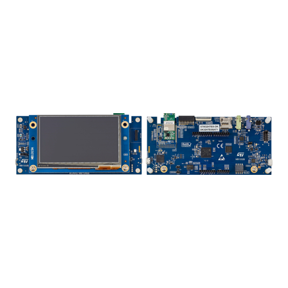
Figure 1.
STM32H7B3I-DK top view
Figure 2.
STM32H7B3I-DK bottom view
Pictures are not contractual.
UM2569 - Rev 1 - December 2019
www.st.com
For further information contact your local STMicroelectronics sales office.
Advertisement
Table of Contents

Related Manuals for ST STM32H7B3I-DK


Summary of Contents for ST STM32H7B3I-DK
-
Page 1: Figure 1. Stm32H7B3I-Dk Top View
DFSDM (8 channels / 8 filters), one USB HS OTG and one USB FS OTG, DCMI interface, FMC interface, TFT LCD controller interface, JTAG, and SWD debugging support. This STM32H7B3I-DK Discovery kit offers everything required for users to get started quickly and develop applications easily. ™... -
Page 2: Features
– External I C expansion connector • Flexible power-supply options: – ST-LINK USB V , USB OTG HS connector, or external sources • On-board STLINK-V3E debugger/programmer with USB re-enumeration capability: mass storage, Virtual COM port, and debug port • Comprehensive free software libraries and examples available with the STM32Cube MCU Package ™... -
Page 3: Ordering Information
Evaluation tools marked as “ES” or “E” are not yet qualified and therefore not ready to be used as reference design or in production. Any consequences deriving from such usage will not be at ST charge. In no event, ST will be liable for any customer usage of these engineering sample tools as reference designs or in production. -
Page 4: Development Environment
STM32 Flash memory for easy demonstration of the device peripherals in standalone mode. The latest versions of the demonstration source code and associated documentation can be downloaded from www.st.com. UM2569 - Rev 1 page 4/54... -
Page 5: Conventions
UM2569 Conventions Conventions Table 3 provides the conventions used for the ON and OFF settings in the present document. Table 3. ON/OFF convention Convention Definition Jumper JPx ON Jumper fitted Jumper JPx OFF Jumper not fitted Jumper JPx [1-2] Jumper should be fitted between Pin 1 and Pin 2 Solder bridge SBx ON SBx connections closed by 0 Ω... -
Page 6: Delivery Recommendations
UM2569 Delivery recommendations Delivery recommendations Before the first use, make sure that no damage occurred to the board during shipment and no socketed components are not firmly fixed in their sockets or loose in the plastic bag. In particular, pay attention to the following component: •... -
Page 7: Getting Started
Ensure that the JP1 jumper is set to STLK. Connect a Type-A to Micro-B USB cable from the STM32H7B3I-DK board (Connect USB STLINK CN14) to a PC to power the board. Then LD5 (+5V) and LD4 (STLINK COM) light up. -
Page 8: Technology Partners
UM2569 Technology partners Technology partners MACRONIX: 512-Mbit Octo-SPI NOR Flash memory device, part number MX25LM51245GXDI00 UM2569 - Rev 1 page 8/54... -
Page 9: Hardware Layout And Configuration
UM2569 Hardware layout and configuration Hardware layout and configuration The STM32H7B3I-DK Discovery kit is designed around the STM32H7B3LIH6QU target microcontroller packaged in TFBGA225. The hardware block diagram, shown in Figure 3, illustrates the STM32H7B3LIH6QU connections with the peripheral components. Figure 4... -
Page 10: Figure 4. Stm32H7B3I-Dk Pcb Layout (Top View)
UM2569 Hardware layout and configuration Figure 4. STM32H7B3I-DK PCB layout (top view) Audio Reset TFT LCD connector button connector B2 User button CN12 connector switch STLINK-V3E COM LED Figure 5. STM32H7B3I-DK PCB layout (bottom view) CN10 and CN11 Audio out ®... -
Page 11: Figure 6. Stm32H7B3I-Dk Board Mechanical Dimensions (Top View, In Millimeters)
UM2569 Hardware layout and configuration Figure 6 Figure 7 provide the mechanical dimensions of the STM32H7B3I-DK board. Figure 6. STM32H7B3I-DK board mechanical dimensions (top view, in millimeters) Figure 7. STM32H7B3I-DK board mechanical dimensions (bottom view, in millimeters) UM2569 - Rev 1... -
Page 12: Embedded Stlink-V3E
Green LED ON: 5V enabled (LD5) 8.1.2 Drivers Before connecting the STM32H7B3I-DK board to a Windows PC via USB, the user must install a driver for the STLINK-V3E (not required for Windows 10). It is available on the www.st.com website. -
Page 13: Stlink-V3E Firmware Upgrade
STM32H7B3I-DK Discovery kit and periodically, to stay up-to-date with the latest firmware version. 8.1.4 Using an external debug tool to program and debug the onboard STM32 There are two basic ways to support an external debug tool: Keep the embedded STLINK-V3E running. -
Page 14: Power Supply
If an overcurrent (more than 500mA) occurs onboard, the RED LED LD7 is lit. The STM32H7B3I-DK board with its shield can be powered from the STLINK-V3E USB connector CN14, but only ST-LINK circuit gets power before USB enumeration because the host PC only provides 100mA to the board at that time. -
Page 15: Supplying The Stm32H7B3I-Dk Using The External Power Supply Input From Vin (7 To 12 V, 800Ma Max)
Supplying the STM32H7B3I-DK using the external power supply input from VIN (7 to 12 V, 800mA max) It can happen that the STM32H7B3I-DK board requires more than 500 mA of supply current. In such a case, the ® board can be supplied through pin8 (marked VIN on the board) of the CN19 ARDUINO connector. -
Page 16: Mcu Power Supply - Smps/Ldo Configuration
UM2569 Power supply 8.2.5 MCU power supply – SMPS/LDO configuration Figure 10. MCU power: SMPS/LDO UM2569 - Rev 1 page 16/54... -
Page 17: Figure 11. Config1 - Ldo Only
UM2569 Power supply The STM32H7B3I-DK board supports four “SMPS/LDO” configurations of STM32H7B3LIH6QU microcontroller, given in the figures below. Figure 11. Config1 - LDO only Figure 12. Config2 - SMPS only (default) UM2569 - Rev 1 page 17/54... -
Page 18: Table 8. Internal Smps / Ldo And Board Configuration
Config3 - SMPS and LDO cascaded Figure 14. Config4 - External SMPS To change the power supply configuration, some reworks are needed on the STM32H7B3I-DK board as detailed in the table below. Table 8. Internal SMPS / LDO and board configuration... -
Page 19: Measurement Of Mcu Current Consumption
UM2569 Measurement of MCU current consumption Config3 Config2 Config4 Config1 (SMPS and LDO SMPS ON (External SMPS) cascaded) SMPS OFF LDO OFF SMPS ON SMPS ON LDO ON (Default config) LDO ON LDO ON SB37 SB38 2.2 uF 100 nF 2.2 uF 2.2 uF 2.2 uF... -
Page 20: Clock Source
USB host when the STM32H7B3I-DK board works as a USB device. The red LED LD8 is lit when an overcurrent occurs (Higher than 500 mA). Note: The STM32H7B3I-DK board can be powered by the CN15 USB connector at 5 V DC with 500 mA current limitation. 8.6.3... -
Page 21: Audio
MACRONIX), which is connected to the OCTOSPI1 interface of the STM32H7B3LIH6QU microcontroller. MX25LM51245GXDI00 operates in a single transfer rate (STR) or a double transfer rate (DTR) mode. The RESETn of the Flash memory is connected to the general reset (NRST) of the STM32H7B3I-DK Discovery kit. 8.6.8... -
Page 22: Virtual Com Port
1 stop bit • No flow control 8.6.10 A CN12 TAG interface footprint is reserved on the STM32H7B3I-DK board, which can be used to debug and program the board. 8.6.11 Buttons and LEDs The black button B1 located on the top side is the reset of the STM32H7B3LIH6QU microcontroller. -
Page 23: Wi-Fi ® Rf Module
The main features of the Inventek ISM43340- M4G-L44-10CF module are: • Based on CYW43340 Cypress Leading Edge Radio Device • Includes STM32F405 ST Cortex M4 Microcontroller • Hardware supported by Cypress WICED SDK 3.5.2 or later • IEEE 802.11b (DSSS 11 Mbit/s) •... -
Page 24: Table 11. Wi-Fi ® - Solder Bridge Configuration
1. The default configuration is shown in bold. Note: In STM32H7B3I-DK boards labeled A1945xxxx, the ISM43340-M4G-L44-10CF is loaded with the C3.5.2.6.STM.BETA4 version which allows a network scan only once. A new version of the ISM43340-M4G-L44-10CF firmware named C3.5.2.6.STM that fixes this limitation is available on the www.st.com... -
Page 25: Board Connectors
The CN14 USB connector is used to connect the embedded STLINK-V3E to the PC for programming and debugging purposes. Figure 16. CN14 Micro-B connector (Front view) The related pinout for the USB ST-LINK connector is listed in Table Table 12. CN14 USB Micro-B connector pinout... -
Page 26: Table 13. Cn15 Usb Otg Hs Micro-Ab Connector Pinout
UM2569 CN15 USB OTG HS Micro-AB connector CN15 USB OTG HS Micro-AB connector A USB OTG high-speed communication link is available at CN15 USB Micro-AB receptacle connector. Micro-AB receptacle enables USB Host and USB Device features. Figure 17. CN15 USB OTG HS Micro-AB connector (Front view) The related pinout for the USB OTG HS connector is listed in Table Table 13. -
Page 27: Cn4 Microsd™ Card Connector
UM2569 CN4 microSD™ card connector CN4 microSD™ card connector ™ microSD cards with 4 GB or more capacity can be inserted in the receptacle CN4. Four data bits of the SDIO1 ™ interface, CLK and CMD signals of the STM32H7B3LIH6QU are used to communicate with the microSD card. -
Page 28: P1 Stmod+ Connector
The standard 20-pin STMod+ connector is available on the STM32H7B3I-DK board to increase compatibility with external boards and modules from the Ecosystem of microcontrollers. By default, it is designed to support an ST- dedicated fanout board to connect different modules or board extensions from different manufacturers. -
Page 29: Cn7 Camera Module Connector
CN7 camera module connector CN7 camera module connector On the STM32H7B3I-DK board, a 30-pin CN7 connector with Digital Camera Interface DCMI signals is available to connect an 8-bit camera module such as the STM32F4DIS-CAM module. This module must be connected with caution before powering the STM32H7B3I-DK board. -
Page 30: Cn12 Tag Connector
UM2569 CN12 TAG connector Pin number Description Pin number Description I2C4_SCL (PD12) DCMI_PIXCLK (PA6) VDD (3V3) CN12 TAG connector The CN12 TAG connector footprint is used to connect STM32H7B3LIH6QU microcontroller for programming or debugging the board. Figure 21. CN12 TAG connector Table 17. -
Page 31: Cn3 Audio Connector
The MB1299 embeds five digital MEMS microphones MP34DT01TR-M from STMicroelectronics. Limitations: On the STM32H7B3I-DK board, some DFSDM signals are shared with STMod+ signals. As a consequence, the user must make sure that nothing is connected to the P1 STMod+ connector (Pins 17 and 19). Table 20. -
Page 32: Table 21. Cn3 Audio Connector Pinout
UM2569 CN3 audio connector Table 21. CN3 audio connector pinout Pin number Function / MCU port Pin number Function / MCU port DFSDM1_2_CKOUT (PB0) DFSDM1_2_CKOUT (PB0) DFSDM1_DATIN7 (PB9) DFSDM1_2_DATIN1 (PB12) DFSDM1_DATIN3 (PC7) DETECTn (PI6) MEMS_LED (PH15) UM2569 - Rev 1 page 32/54... -
Page 33: Cn1 Tft Lcd Display Connector
UM2569 CN1 TFT LCD display connector CN1 TFT LCD display connector The CN1 connector is designed to connect the 4.3-inch TFT LCD touchscreen board. Table 22 shows the assignment of CN1 and STM32H7B3LIH6QU terminals. Figure 24. CN1 TFT LCD display connector Table 22. -
Page 34: Cn10, Cn11, Cn19, And Cn20 Arduino® Uno V3 Connectors
PD12 I2C4_SCL 1. The 3V3 on ARD connector pin 4 of CN19 is not a power input for the STM32H7B3I-DK board, to simplify power architecture. 2. The external voltage applied to pin VIN on pin 8 of CN19 must be in the range 6 to 9V at 25°C ambient temperature. If a higher voltage is applied on the regulator U15, it may overheat and could be damaged. -
Page 35: Cn5 Audio Green Jack - Line Out
SPK_L (33 Ω typical) 9.12 CN6 audio blue jack - line in A 3.5 mm stereo audio blue jack output CN6 is available on the STM32H7B3I-DK board for audio line input. Figure 26. CN6 stereo headset with a microphone jack... -
Page 36: Table 25. Cn5 Audio Jack Connector Pinout (Onboard)
UM2569 CN6 audio blue jack - line in Table 25. CN5 audio jack connector pinout (Onboard) Pin number Description Stereo headset with microphone pinning OUT_Right SPK_R (33 Ω typical) OUT_Left SPK_L (33 Ω typical) UM2569 - Rev 1 page 36/54... -
Page 37: Appendix Astm32H7B3I-Dk I/O Assignment
UM2569 STM32H7B3I-DK I/O assignment Appendix A STM32H7B3I-DK I/O assignment Table 26. STM32H7B3I-DK I/O assignment Pin number GPIO port Signal or label Comment I2S6_WS USART2_CTS PMOD1-CTS LCD_BL_CTRL LCD_ON/OFF ULPI_D0 I2S6_MCK DCMI_HSYNC PMOD13-ADC ADC1_INP18 ARD_A0 ULPI_CK DCMI_PIXCLK DCMI_PWR_EN MCO1 USART1_TX PA10 USART1_RX... - Page 38 UM2569 STM32H7B3I-DK I/O assignment Pin number GPIO port Signal or label Comment DFSDM1_2_DATIN1 PB13 ULPI_D6 PMOD9-MISOs PB14 SPI2_MISO ARD_D12 PMOD8-MOSIs SPI2_MOSI PB15 ARD_D11 TIM1_CH3N ULPI_STP OCSPI1_IO4 PMOD3-MISOp SPI2_MISO PMOD2-MOSIp SPI2_MOSI ARD_A1 ADC12_INP4 OCSPI1_DQS PMOD11-INT PMOD17-DF-D3 DFSDM1_DATIN3 SDIO1_D0 SDIO1_D1 DCMI_D3 PC10...
- Page 39 UM2569 STM32H7B3I-DK I/O assignment Pin number GPIO port Signal or label Comment FMC_NBL0 FMC_NBL1 ARD_D4 SAI1_SD_B SAI1_FS_A SAI1_SCK_A SAI1_SD_A FMC_D4 FMC_D5 FMC_D6 PE10 FMC_D7 PE11 FMC_D8 PE12 FMC_D9 PE13 FMC_D10 PE14 FMC_D11 PE15 FMC_D12 FMC_A0 FMC_A1 FMC_A2 FMC_A3 FMC_A4 FMC_A5...
- Page 40 UM2569 STM32H7B3I-DK I/O assignment Pin number GPIO port Signal or label Comment FMC_SDCLK OCSPI1_IO6 PG10 DCMI_D2 PG11 USER_LED1 PG12 I2S6_SDI PG13 I2S6_CK PG14 I2S6_SDO PG15 FMC_SDNCAS OSC_IN OSC_OUT LCD_INT OCSPI1_IO5 ULPI_NXT FMC_SDNWE FMC_SDNE1 FMC_SDCKE1 PMOD12-RST ll FDCAN_STBY ARD_D3 TIM12_CH2 PH10...
- Page 41 UM2569 STM32H7B3I-DK I/O assignment Pin number GPIO port Signal or label Comment PI15 LCD_R0 LCD_R1 LCD_R2 LCD_R3 LCD_R4 LCD_R5 LCD_R6 LCD_R7 LCD_G0 LCD_G1 LCD_G2 PJ10 LCD_G3 PJ11 LCD_G4 PJ12 LCD_B0 PJ13 LCD_B1 PJ14 LCD_B2 PJ15 LCD_B3 LCD_G5 LCD_G6 LCD_G7 LCD_B4...
-
Page 42: Appendix B Fanout Board (Mb1280)
Fanout board (MB1280) The fanout board, shown in Figure 29, is included in the STM32H7B3I-DK Discovery kit. It can be connected to P1 STMod+ connector and it provides access to: • MikroElektronika Click board compatible connectors (MB1280 CN10 and CN11: two 1x8-pin female connectors) •... -
Page 43: Esp-01 Wi-Fi ® Board Compatible Connector
UM2569 ESP-01 Wi‑Fi® board compatible connector ® ESP-01 Wi‑Fi board compatible connector ® The ESP-01 Wi‑Fi board connector is 2.54"-pitch with 2x4-pin female connectors. Table 28 shows the definition of the pins. ® Table 28. Description of the ESP-01 Wi‑Fi connector pins STMod+ connector number ESP-01 function... -
Page 44: Appendix Cstmod+ Gpio Sharing And Multiplexing
UM2569 STMod+ GPIO sharing and multiplexing Appendix C STMod+ GPIO sharing and multiplexing Table 31 gives the description of the signals available on the STMod+ connector. It also shows which signal is ® ® shared with other board connectors (such as camera, ARDUINO Uno V3, DFSDM or Wi‑Fi ). -
Page 45: Table 31. Stmod+ Gpio Sharing And Multiplexing
Table 31. STMod+ GPIO sharing and multiplexing Shared or exclusive functions STMod+ Shared or exclusive functions Wi‑Fi ® Some other alternate functions Basic Port Pins Port Basic Some other alternate functions DFSDM DCMI CTS2 TIM2_CH1, TIM2_ETR, TIM5_CH1, TIM8_ETR, SPI6_NSS, USART2_NSS, UART4_TX, [ADC1_INP16] CTS2 TIM3_CH1, TIM8_CH1, USART6_TX NSS2... -
Page 46: Appendix D Federal Communications Commission (Fcc) And Industry Canada (Ic)
Federal Communications Commission (FCC) and Industry Canada (IC) Compliance Statements Appendix D Federal Communications Commission (FCC) and Industry Canada (IC) Compliance Statements Applicable for STM32H7B3I-DK Discovery kit products with order code STM32H7B3I-DK (containing ISM43340- M4G-L44-10CF module). FCC Compliance Statement FCC Compliance Statement Contains FCC ID: O7P-341 Part 15.19... - Page 47 UM2569 IC Compliance Statement Appareils radio exempts de licence (ISDE) L’émetteur/récepteur exempt de licence contenu dans le présent appareil est conforme aux CNR d’Innovation, Sciences et Développement économique Canada applicables aux appareils radio exempts de licence. L’exploitation est autorisée aux deux conditions suivantes: L’appareil ne doit pas produire de brouillage;...
-
Page 48: Revision History
UM2569 Revision history Table 32. Document revision history Date Revision Changes 19-Dec-2019 Initial release UM2569 - Rev 1 page 48/54... -
Page 49: Table Of Contents
800mA max) ............15 8.2.3 Supplying the STM32H7B3I-DK using USB charger (5 V)......15 8.2.4 Supplying the STM32H7B3I-DK using USB OTG HS connector (5 V / 500 mA) . - Page 50 STM32H7B3I-DK I/O assignment ........
- Page 51 UM2569 Contents Appendix C STMod+ GPIO sharing and multiplexing ........44 Appendix D Federal Communications Commission (FCC) and Industry Canada (IC) Compliance Statements.
-
Page 52: List Of Tables
STM32H7B3I-DK I/O assignment........ -
Page 53: List Of Figures
STM32H7B3I-DK PCB layout (bottom view) ..........10 Figure 6. STM32H7B3I-DK board mechanical dimensions (top view, in millimeters) ......11 Figure 7. - Page 54 ST’s terms and conditions of sale in place at the time of order acknowledgement. Purchasers are solely responsible for the choice, selection, and use of ST products and ST assumes no liability for application assistance or the design of Purchasers’...
Need help?
Do you have a question about the STM32H7B3I-DK and is the answer not in the manual?
Questions and answers