
Subscribe to Our Youtube Channel
Related Manuals for Atmel STK502


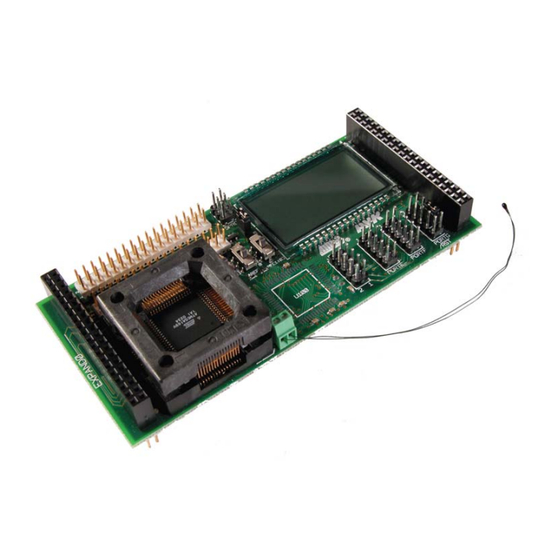
Summary of Contents for Atmel STK502
- Page 1 STK502 User Guide...
-
Page 3: Table Of Contents
STK502 User Guide Table of Contents Section 1 Introduction ... 1-1 Section 2 Using the STK502 Top Module... 2-1 Connecting the STK502 to the STK500 Starter Kit ...2-1 2.1.1 Placing an ATmega169 on STK502 ...2-1 PORT Connectors...2-2 2.2.1 PORT E/PORT F ...2-2 2.2.2... - Page 4 Table of Contents 2528A–AVR–11/02 Section 5 Technical Support... 5-1 Section 6 Complete Schematics... 6-1 STK502 User Guide...
-
Page 5: Introduction
Section 1 Introduction The STK502 board is a top module designed to add ATmega169 support to the STK500 development board from Atmel Corporation. STK502 includes connectors and hardware allowing full utilization of the new features of the ATmega169. The Zero Insertion Force (ZIF) socket makes it easy to use of TQFP packages for prototyping. - Page 6 Quick Reference to all Switches and Jumpers in the Silk-Screen of the PCB. Pre-programmed ATmega169 with Demonstration Application. Includes C-code Examples for all Major Peripherals on the ATmega169 Device. – The Way to Get Going with your ATmega169 STK502 User Guide...
-
Page 7: Using The Stk502 Top Module
This section describes in detail how the STK502 is used with the STK500. Connect STK502 to the STK500 expansion header 0 and 1. It is important that the top module is connected in the correct orientation as shown in Figure 2-1. EXPAND0 written on the STK502 top module should match EXPAND0 written beside the expansion header on the STK500 board. -
Page 8: Port Connectors
2528A–AVR–11/02 Figure 2-2. Pin1 on ZIF Socket and TQFP Footprint Caution: Do not mount an ATmega169 on the STK502 at the same time as an AVR is mounted on the STK500 board. Neither of the devices will work as intended. -
Page 9: Port G/Rst
RESET-signal that comes from the STK500 board. Please note that it is not directly con- nected to the ZIF socket or the TQFP footprint on the STK502. This because the RESET-signal on the STK500 has an pull-up resistor to VCCT which will interfere with PG5 when used as an ordinary I/O-pin. -
Page 10: Programming The Atmega169
To program the ATmega169 using ISP Programming mode, connect the 6-wire cable between the ISP6PIN connector on the STK500 board and the ISP connector on the STK502 board as shown in Figure 2-6. The device can be programmed using the Serial Programming mode in the AVR Studio4 STK500 software. -
Page 11: High-Voltage Programming
To program the ATmega169 using High-voltage (Parallel) Programming, connect the PROGCTRL to PORTD and PROGDATA to PORTB on the STK500 as shown in Figure 2-7. Make sure that the TOSC-switch is placed in the XTAL position. See Section 2.6, “TOSC Switch”. -
Page 12: Jtag Connector
JTAG Connector 2528A–AVR–11/02 Figure 2-8 shows how to connect the JTAG ICE probe on the STK502 board. Figure 2-8. Connecting JTAG ICE to the STK502 The JTAG connector is used for the ATmega169 built-in JTAG interface. The pin out of the connector is shown in Figure 2-9 and is compliant with the pin out of the JTAG ICE available from Atmel. -
Page 13: Technical Specifications
ATmega169”. The header next to it, labelled “STK502 LCD pins” holds all the segments-pins for the LCD-display on the STK502. By using the 34-lead cable that comes with the STK502-kit, the two pin-headers can be connected, allowing the ATmega169 to control the LCD-display. See Figure 2-10. - Page 14 Seg. M169 This hardware configuration will give a certain bit-mapping between the bits in the ATmega169 LCDDRx Register and the segments on the STK502 LCD. See Section 4.1 “STK502 LCD Bit Mappings” With the header J300 labelled “19 24” one can connect LCD-pin 24 (which is default unconnected) to LCD-pin 19 by the use of a jumper.
- Page 15 Make sure the display is compatible with the electrical characteristics on the ATmega169. For more information on how to write software for the LCD-display see application note “AVR064: STK502 – A Temperature Monitoring System with LCD Output” and applica- tion note “AVR065: LCD Driver for the STK502 LCD”. Note: The LCD-display on the STK502 can be ordered separately from ACTE Norway (www.acte.no).
-
Page 16: Tosc Switch
On the ATmega169 the TOSC1 and TOSC2 lines are shared with XTAL1 and XTAL2. The TOSC switch selects whether the 32 kHz crystal on the STK502, or the XT1/XT2 signals from STK500 should be connected to these pins on the device. -
Page 17: Sensor
“AVR064: STK502 – A Temperature Monitoring System with LCD Output” describes the details of the application. Two switches on the STK502 are used to connect the sensor to the ADC-channels on the ATmega169 as shown in Figure 2-17. - Page 18 2 Positions: PIN: In this position the PF0 and PF1 are from the PORTF on the STK502 are connected to the PF0 and PF1 on the ATmega169. Default position. Sensor: In this position the pin 1 from the screw-terminal on the STK502 are connected to PF0 on the ATmega169, and the pin 2 from the screw-terminal are connected to PF1 on the ATmega169.
-
Page 19: Troubleshooting Guide
STK502 User Guide Troubleshooting Guide Table 3-1. Troubleshooting Guide Problem Reason The LCD is not connected. Nothing is displayed on The LCD is not enabled in the LCD. the AVR device. The update frequency is not correct. The PORTA/C/D and/or G... - Page 20 ATmega169. Note: 1. See the application note “AVR065: LCD Driver for the STK502 LCD” on how to con- trol the LCD-display or the the application note “AVR064: STK502 – A Temperature Monitoring System with LCD Output”. Solution Please refer to Figure 2-7 for correct Parallel Programming setup.
-
Page 21: Technical Specifications
Operation voltage ........... . 3V STK502 User Guide... - Page 22 Technical Specifications Figure 4-1. Layout for the STK502 LCD-display STK502 User Guide 2528A–AVR–11/02...
-
Page 23: Stk502 Lcd Bit Mappings
Backplane Control Lines (also known as Common Lines). The LCD on the STK502 uses all four Common Lines and all 25 segments, in total 4 x 25 = 100 seg- ments. As can be seen in the LCD data sheet (Figure 4-1) describing the internal connection of pins, Common Lines and segments, the alphanumeric digits are referred to with a number according to where they are located on the LCD. -
Page 24: Alphanumeric Digit Number Six
The bit mappings for the alphanumeric digit number seven are listed below. Table 4-6. Bit Mappings for LCD Alphanumeric Digit Number Seven Register Name Bit7 Bit6 LCDDR2 LCDDR7 LCDDR12 LCDDR17 Bit5 Bit4 Bit3 Bit2 Bit1 Bit5 Bit4 Bit3 Bit2 Bit1 STK502 User Guide Bit0 Bit0... -
Page 25: Technical Support
STK502 User Guide For Technical support, please contact avr@atmel.com. When requesting technical sup- port, please include the following information: Which target AVR device is used (complete part number). Target voltage and speed. Clock source and fuse setting of the AVR. - Page 26 Technical Support STK502 User Guide 2528A–AVR–11/02...
-
Page 27: Complete Schematics
Section 6 Complete Schematics On the following pages the complete schematics and assembly drawing of the STK502 revision B are shown. STK502 User Guide Rev. 2528A–AVR–11/02... - Page 28 PD0(ICP/SEG22) (TCK/ADC4)PF4 XTAL1(TOSC1) (ADC3)PF3 XTAL2(TOSC2) (ADC2)PF2 (ADC1)PF1 (ADC0)PF0 PG5(RESET) AREF PG4(T0/SEG23) AGND PG3(T1/SEG24) AVCC PB7(OC2) PDT7 PDT6 PDT5 PDT4 PDT3 PDT2 PDT1 PDT0 PGT5 PGT4 PGT3 PDT7 PDT6 PDT5 PDT4 PDT3 PDT2 PDT1 PDT0 PGT5 PGT4 PGT3 STK502 User Guide...
- Page 29 Figure 6-2. Schematics, 2 of 3 MOUNTED STK502 User Guide PBT2 PBT3 PBT1 Complete Schematics 2528A–AVR–11/02...
- Page 30 Complete Schematics Figure 6-3. Schematics, 3 of 3 2528A–AVR–11/02 STK502 User Guide...
- Page 31 Complete Schematics Figure 6-4. Assembly Drawing, 1 of 1 STK502 User Guide 2528A–AVR–11/02...
- Page 32 Complete Schematics STK502 User Guide 2528A–AVR–11/02...
- Page 33 No licenses to patents or other intellectual property of Atmel are granted by the Company in connection with the sale of Atmel products, expressly or by implication. Atmel’s products are not authorized for use as critical components in life support devices or systems.
Need help?
Do you have a question about the STK502 and is the answer not in the manual?
Questions and answers