
Related Manuals for Atmel AT89LP


Summary of Contents for Atmel AT89LP
- Page 1 AT89LP OCD Developer Board 3.0 ........................User Guide 3720A–MICRO–2/11...
-
Page 2: Table Of Contents
Mode Select (J5, J6, J7, J10, J11) ..............3-4 3.5.3 Reset Recovery (J1) .................... 3-4 3.5.4 DDA Select (J3) ....................3-5 3.5.5 SCK Select (J2) ....................3-6 Using as a Daughter Board....................3-6 Section 4 Board Description....................... 4-1 AT89LP OCD Developer Board 3.0 User Guide 3720A–MICRO–2/11... - Page 3 Board Layout........................4-1 Board Schematic........................ 4-3 Bill of Materials........................4-4 Section 5 Troubleshooting ......................5-1 Section 6 Revision History......................6-1 Revision History ......................... 6-1 AT89LP OCD Developer Board 3.0 User Guide 1-ii 3720A–MICRO–2/11...
- Page 4 1-iii AT89LP OCD Developer Board 3.0 User Guide 3720A–MICRO–2/11...
-
Page 5: Getting Started
AT89LP OCD Developer board. Get the Software The first step in using the OCD board is to obtain and install the AT89LP Developer Studio IDE. This software can communicate with the OCD board to program the target device and control its execution via the OCD interface. -
Page 6: Program The Target
1.2.2 Program the Target Start the AT89LP ISP Studio application and follow these steps. 1. Select Target > Select Target from the menu or click the target icon in the toolbar 2. In the dialog, highlight your device and click on the Select button 3. -
Page 7: Configure Board For Debug
Jumper settings for OCD Pair with Another Development Board The AT89LP OCD Developer Board is a low-cost board and as such has limited development resources. For best results it needs to be paired with another fully featured development board. Two configurations are possible: either connect the two boards by cable or piggyback the OCD board on a development board through a PDIP socket. -
Page 8: Cable Connection
NOT be mounted in one of the OCD Board sockets. 1.4.2 Daughter Board For target boards that do not support an Atmel 10-pin header the OCD board can piggyback on the tar- get board as a daughter board as shown in Figure 1-3. -
Page 9: Start The Debugger
Getting Started Start the Debugger Once you have some source code in AT89LP Developer Studio, follow these steps to build, connect and debug your code on the OCD board. 1. Select Debug > Build Solution from the menu or click the build icon in the toolbar 2. - Page 10 Getting Started AT89LP OCD Developer Board 3.0 User Guide 3720A–MICRO–2/11...
-
Page 11: Introduction
AT89LP OCD Developer Board allows users to develop and debug their code and prototype their designs. The board was designed to be used with the Atmel AT89LP single-cycle 8051 microcon- trollers along with the Atmel AT89LP Developer Studio, an Integrated Development Environment (IDE). - Page 12 Introduction AT89LP OCD Developer Board 3.0 User Guide 3720A–MICRO–2/11...
-
Page 13: Hardware Description
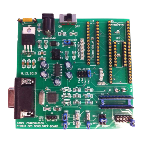
Board Overview Figure 3.1.1 shows the AT89LP OCD Developer Board. Figure 3-1. The AT89LP OCD Developer Board. 3.1.1 Block Diagram Figure 3.2 shows the functional block diagram of the AT89LP OCD Developer Board. AT89LP OCD Developer Board 3.0 User Guide 3720A–MICRO–2/11... -
Page 14: Power Supply
Target Power Supply The AT89LP OCD Developer Board has an on-board voltage regulator to supply power to the board. This regulator requires a 9VDC external power source connected to the 2.1mm male jack outlet. No spe- cific polarization is mandatory as the on-board diode rectifier provides protection against inadvertent polarization insertion. -
Page 15: Ocd/Isp Header
The header can be connected to an equivalent header on a target board through a 10-pin ribbon cable such as the Atmel AT89ISP cable. When using the OCD board with an external target board, all target devices must be removed from sockets U3, U4 and U5 on the OCD board or you can permanently damage the target devices and/or development board. -
Page 16: Mode Select (J5, J6, J7, J10, J11)
3.5.3 Reset Recovery (J1) AT89LP devices have fuses to enable/disable both OCD and ISP. If OCD is enabled or ISP is disabled, the RST pin cannot be used to enter programming mode during a warm reset. In these cases program- ming mode is activated only if RST is forced active at cold power-up. -
Page 17: Dda Select (J3)
J3 is located near the lower left corner of the 28DIP socket U4 as shownin Figure 3-10. Figure 3-9. J3 DDA Selection Settings Crystal External (AT89LP428/828) Clock Strap Crystal Internal (AT89LP3240/6440) Oscillator Jumper Header AT89LP OCD Developer Board 3.0 User Guide 3720A–MICRO–2/11... -
Page 18: Sck Select (J2)
OCD board on a development board through a PDIP socket. For target boards that do not support an Atmel 10-pin header the OCD board can piggyback on the target board as a daughter board as shown in Figure 3-12. - Page 19 Figure 3-12. AT89LP OCD Developer Board as Daughter Board For this configuration to work the following requirements must be met. The target socket on the AT89LP OCD Developer board must be built with lead extensions on the reverse side as shown in Figure 3-13 so that it can plug directly into another socket.
- Page 20 Hardware Description AT89LP OCD Developer Board 3.0 User Guide 3720A–MICRO–2/11...
-
Page 21: Board Description
Section 4 Board Description Board Layout The PCB layout layers for the AT89LP OCD Developer version 3.0 are provided here for reference. Elec- tronic Gerber files and OrCAD schematics can be found at: http://www.atmel.com/dyn/resources/prod_documents/LP_Studio_Board.zip Figure 4-1. Silk Layer AT89LP OCD Developer Board 3.0 User Guide... - Page 22 Board Description Figure 4-2. Top Layer Figure 4-3. Bottom Layer AT89LP OCD Developer Board 3.0 User Guide 3720A–MICRO–2/11...
-
Page 23: Board Schematic
Board Description Board Schematic Figure 4-4. AT89LP OCD Developer Board Schematic AT89LP OCD Developer Board 3.0 User Guide 3720A–MICRO–2/11... -
Page 24: Bill Of Materials
Board Description Bill of Materials Table 4-1. Bill of Materials for AT89LP OCD Developer Board 3.0 Comment Footprint Designators Notes .1uF 0603 Non-Polarized .1uF 0603 Non-Polarized .1uF 0603 Non-Polarized .1uF 0603 Non-Polarized .1uF CAP_5MM Non-Polarized .1uF CAP_5MM Non-Polarized .1uF CAP_5MM Non-Polarized .1uF... - Page 25 Board Description Table 4-1. Bill of Materials for AT89LP OCD Developer Board 3.0 Comment Footprint Designators Notes SW SPST SPDT RST_RCVRY 3x2 Header SCK_SLCT 3PIN Header DDA_SELECT 4x2 Header VCC Select 3PIN Header 10ISP_OSCD AT89ISP_OCD AT89LP216 DIP 16 AT89LP6440 DIP 40...
- Page 26 Board Description AT89LP OCD Developer Board 3.0 User Guide 3720A–MICRO–2/11...
-
Page 27: Troubleshooting
ISP will function correctly 2. In some target configurations prgramming is only possible by forcing the reset active at power-up. Section 3.5.3 on page 3-4 on using jumper J1 to force the reset AT89LP OCD Developer Board 3.0 User Guide 3720A–MICRO–2/11... - Page 28 Troubleshooting AT89LP OCD Developer Board 3.0 User Guide 3720A–MICRO–2/11...
-
Page 29: Revision History
Section 6 Revision History Revision History Revision No. History • Revision A – February 2011 Initial Release AT89LP OCD Developer Board 3.0 User Guide 3720A–MICRO–2/11... - Page 30 Revision History AT89LP OCD Developer Board 3.0 User Guide 3720A–MICRO–2/11...
- Page 31 Disclaimer: The information in this document is provided in connection with Atmel products. No license, express or implied, by estoppel or otherwise, to any intellectual property right is granted by this document or in connection with the sale of Atmel products. EXCEPT AS SET FORTH IN ATMEL’S TERMS AND CONDI- TIONS OF SALE LOCATED ON ATMEL’S WEB SITE, ATMEL ASSUMES NO LIABILITY WHATSOEVER AND DISCLAIMS ANY EXPRESS, IMPLIED OR STATUTORY...
Need help?
Do you have a question about the AT89LP and is the answer not in the manual?
Questions and answers