Advertisement
Quick Links
Download this manual
See also:
Programming Manual
AN685
L
D
G
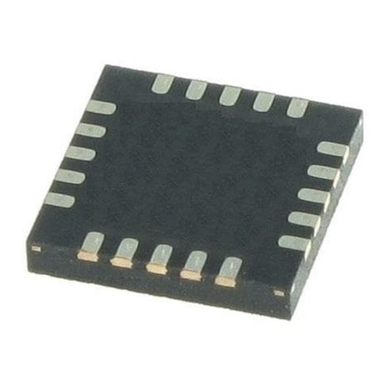
Si4455/435
RF IC
AYOUT
E S I G N
U I D E FOR THE
X
S
1. Introduction
This application note provides guidelines and design examples to help users design PCBs for the next generation
EZRadio® RF ICs, such as the Si4455/435x devices, using good design practices that allow for high quality RF
performance. The RF performance and the critical maximum peak voltage on the output pin strongly depends on
the PCB layout as well as the design of the matching networks. The matching principles are described in detail in
"AN693: Si4455 Low Power PA Matching". Furthermore, these types of RF ICs are also applicable in the RF Stick
and RF pico board solutions where a PCB antenna is used, which also requires some considerations in the layout
design. For optimal performance, Silicon Labs recommends using the PCB layout design suggestions described in
the following sections.
2. Design Recommendations when Using Si4455/435x RF ICs
Extensive testing has been completed using reference designs provided by Silicon Labs. It is recommended that
designers use the reference designs "as-is" since they minimize de-tuning effects caused by parasitics and
generated by component placement and PCB routing.
When layouts as shown by the reference designs cannot be followed (as a result of PCB size and shape
limitations), then the following layout design rules are recommended.
The Si4455 transceiver RF chip uses Class-E TX matching network and a 4-element matching balun on the RX
side in Direct Tie configuration (where the TX and RX paths are connected together directly without any additional
RF switch). Meanwhile, the Si435x receiver RF chip uses only the 4-element matching balun.
Rev. 0.4
Copyright © 2014 by Silicon Laboratories
AN685
Advertisement

Related Manuals for Silicon Laboratories Si4455 Series


Summary of Contents for Silicon Laboratories Si4455 Series
- Page 1 Direct Tie configuration (where the TX and RX paths are connected together directly without any additional RF switch). Meanwhile, the Si435x receiver RF chip uses only the 4-element matching balun. Rev. 0.4 Copyright © 2014 by Silicon Laboratories AN685...
-
Page 2: Guidelines For Layout Design When Using The Si4455 Rf Ic
AN685 3. Guidelines for Layout Design when Using the Si4455 RF IC Examples shown in this section are based upon the layout of the 4355-PRXB434M (4355CPRXB434M) pico board. The schematic of the RF part of the Class-E Direct Tie type matching network for the Si4455 chip is shown in Figure 1. - Page 3 AN685 The layout structure of the RF part of the Class-E Direct Tie type matching network is shown in Figure 2. Figure 2. Layout Structure of the RF Part of the Class-E Direct Tie Type Matching Network for Si4455 3.1. Layout Design Guidelines for Si4455 RF IC Some general rules for designing an RF-related layout for good RF performance: ...
- Page 4 AN685 means the RX is further away) in order to reduce the series parasitic inductance which increases the voltage peak at the internal drain pin. The trace parasitics are very critical in case of the connection of LR2; therefore, the shortest traces possible should be used for connecting LR2 to the TX side.
- Page 5 AN685 The smaller VDD bypass capacitors (C4 and C3) should be kept as close to the VDD pins as possible. The exposed pad footprint for the paddle of the RF IC should use as many vias as possible to ensure good grounding and heatsink capability.
- Page 6 AN685 Figure 4 demonstrates the grounding of the RFIC, the VDD filter capacitors and crystal positions, and the isolation between the traces and the ground metal. Figure 4. RFIC GND Vias and GND Metallization To achieve good RF ground on the layout, it is recommended to add large, continuous GND metallization on the top layer in the area of the RF section (at a minimum).
- Page 7 AN685 Figure 5 and Figure 6 demonstrates the 50 coplanartransmission line and theGND metal-filled sections on the RF part of the Si4455-LED-434 (Si4455CLED-434) pico board PCB. The top and bottom layers are shown, respectively. Examples for the 50 grounded coplanar trace dimensions are shown in Table 1. Figure 5.
- Page 8 AN685 Table 1. Parameters for 50 Grounded Coplanar Lines 119-960 MHz 0.018-0.035 mm 1.5 mm 0.26 m 0.25 mm 0.64 mm 1.26 mm 0.45 mm *Note: For the 4-layer PCBs, the thickness between the top and the next inner layer should be taken into account. Figure 7.
- Page 9 AN685 Additional concerns for the RF Stick solutions: The Si4455-LED-xxx (Si4455CLED-xxx) development boards (RFStick solutions) can be optionally broken in two along the connector so that the RF Part can be used as a pico board. Due to this option, the developer must ensure that the ground planes of the RF and MCU sections are connected well as possible to each other.
- Page 10 AN685 For optimal RF performance, it is necessary to have a good connection between the two ground plane sections to ensure as large and continuous a ground plane as possible for the monopole-types antennas. This connection will achieve a good antenna characteristic and the best antenna gain. On the RF Stick there is an option to select between the PCB antenna or the SMA connector (with a 50 ...
-
Page 11: Guidelines For Layout Design When Using The Si435X Rf Ic
AN685 4. Guidelines for Layout Design when Using the Si435x RF IC Examples shown in this section are based on the layout of the 4355-PRXB434M (4355CPRXB434M) pico board. The schematic of the RF part for the Si435x chip is shown in Figure 11. This 4-element matching balun provides a single-ended to differential conversion that matches the LNA input to a 50 ... - Page 12 AN685 Figure 12. RF Layout Structure for the Si4355 Chip 4.1. Layout Design Guidelines for Si435x RF IC The principles in this case are the same as for the Si4455 boards except for the following issues: Because only the RX part is applied in this case (no TX matching), the parallel inductor between the differential ports (LR1) should be placed as close to the RX pins of the RF IC as possible to reduce the series parasitic inductance, which may cause de-tuning effects in the matching network.
- Page 13 AN685 Figure 13. Layout of the RF Part of the Si4355-LED-434 (Si4355CLED-434) Development Board Rev. 0.4...
- Page 14 AN685 5. PCB Antennas for Si4455/Si435x RF ICs This document shows the PCB antenna layouts that are used in Si4455/435x applications. More information about these antennas and descriptions of their operation can be found in the application note, “AN686: Antennas for the Si4455/435x RF ICs”.
- Page 15 AN685 Figure 15. Differential BIFA used in 4455-LED-434 (4455CLED-434) Development Boards The BIFA antenna in Figure 15 with the printed balun transformer has a single-ended 50 input, thus between the antenna and the RF IC a 50 matching network is also required. The printed balun drives a differential BIFA and the impedance match is done by a differential strip line.
- Page 16 AN685 Figure 16. Input impedance of BIFA at 868 MHz One can observe that the input reflection is about –17 dB, which means very good input impedance to 50 . The outdoor range between two modules (Si4455-LED-868 (Si4455CLED-868) development boards) was also under investigation with the follow parameters: ...
-
Page 17: Guidelines For Layout Design When Using The Si4012 Rf Ic
AN685 6. Guidelines for Layout Design when Using the Si4012 RF IC Examples shown in this section are based upon the layout of the 4012-PSC10B434 (4012CPSC10B434) pico boards. The schematic of the RF part for the Si4012 chip is shown in Figure 18. The matching network includes the 4- element matching balun and a 3-element low pass filter (the order of the filter can be changed according to the required suppression of the standard of the used band). - Page 18 AN685 Figure 19. Layout Structure of 4012-PSC10B434 (4012CPSC10B434) Pico Board 6.1. Layout Design Guidelines for the Si4012 RF IC The layout design principles for the Si4012 RF IC, are the same as the Si435x and Si4455 RF ICs with the following additional specific issues: ...
- Page 19 AN685 PPENDIX This section includes references for all the PCB layouts that use the Si4355 or Si4455 RF IC. Figure 20. 4455-PCExxDxxxM (4455CPCExxDxxxM) Pico Board Figure 21. Si4355-LED-434 (Si4355CLED-434) Development Board Rev. 0.4...
- Page 20 AN685 Figure 22. Si4355-LED-868 (Si4355CLED-868) & Si4355-LED-915 (Si4355CLED-915) Development Board Figure 23. Si4355-PRXB434B (4355CPRXB434B) Development Board Rev. 0.4...
-
Page 21: Document Change List
AN685 OCUMENT HANGE Revision 0.3 to Revision 0.4 4455Cyyy in brackets added to 4455-yyy 4355Cyyy in brackets added to 4355-yyy 4012Cyyy in brackets added to 4012-yyy Rev. 0.4... - Page 22 The products must not be used within any Life Support System without the specific written consent of Silicon Laboratories. A "Life Support System" is any product or system intended to support or sustain life and/or health, which, if it fails, can be reasonably expected to result in significant personal injury or death.
Need help?
Do you have a question about the Si4455 Series and is the answer not in the manual?
Questions and answers